The document describes the design, construction, and testing of a Bradbury-Nielsen Gate (BNG) for use in time-of-flight calculations of an electrospray thruster. A 50-wire BNG was constructed with a 3"x3" frame and 2"x2" inner window using Delrin. Experimental testing confirmed the BNG could deflect the ion beam as expected, reducing current by up to 94% when powered on. However, issues with thermal expansion, noise, and the thruster prevented reliable time-of-flight measurements. Future work is needed to address these issues and obtain more precise experimental hardware.
International Journal of Engineering Research and Applications (IJERA) is an open access online peer reviewed international journal that publishes research and review articles in the fields of Computer Science, Neural Networks, Electrical Engineering, Software Engineering, Information Technology, Mechanical Engineering, Chemical Engineering, Plastic Engineering, Food Technology, Textile Engineering, Nano Technology & science, Power Electronics, Electronics & Communication Engineering, Computational mathematics, Image processing, Civil Engineering, Structural Engineering, Environmental Engineering, VLSI Testing & Low Power VLSI Design etc.
Design and Simulation of a Fractal Micro-TransformerIJERA Editor
This document summarizes the design and simulation of a fractal micro-transformer. The researchers designed an air-core fractal micro-transformer using finite element modeling software. Simulation results showed improved performance parameters compared to macro transformers, including higher voltage gain. Electric displacement and magnetic energy density within the micro-transformer were determined to be 2 x 10-11 C/m2 and 100 J/m3 respectively. Losses within the air-core design were minimal at 3 W/m3. The micro-transformer was concluded to be suitable for integration in MEMS and VLSI applications due to its small size, high impedance, and isolation capabilities.
Structural and Optical properties of Multiwalled Carbon Nanotubes Modified by...TELKOMNIKA JOURNAL
Structure, chemical, and physical properties of Multiwalled Carbon Nanotubes (MWCNTs) after
modification by dielectric barrier discharge (DBD) at atmospheric pressure is investigated using
Transmission Electron Microscopy (TEM), Raman and Uv-vis-NIR spectroscopy. Effects of plasma
treatment time on MWCNTs are analyzed. TEM result shows that during the short period of plasma
treatment time of 5 minutes, the tube surface experienced a few damages. With increase in plasma
treatment time, the tube surface is damaged to a certain extent. Intensity ratio, ID/IG through Raman
analysis shows a good agreement with TEM. The values of ID/IG of the modified MWCNTs are larger than
those of pristine MWCNTs. An increase of ID/IG indicates that considerable defects are produced on the
surfaces of MWCNTs. The treated MWCNTs has energy band gap compared to zero band gap of
untreated MWCNTs. It is believed that the defect site of MWCNTs can modify the electronics properties of
MWCNTs from being metallic to semiconducting structure, which is applicable for almost all electronics
device applications.
The driving engine for the exponential growth of digital information processing systems is scaling down the transistor dimensions. For decades, this has enhanced the device performance and density. However, the International Technology Roadmap for Semiconductors (ITRS) states the end of Moore’s law in the next decade due to the scaling challenges of silicon-based CMOS electronics, e.g. extremely high power density. The forward-looking solutions are the utilization of emerging materials and devices for integrated circuits, e.g. carbon-based materials. The presentation of my Ph.D. work focuses on graphene, one atomic layer of carbon sheet, experimentally discovered in 2004. Since fabrication technology of emerging materials is still in early stages, transistor modeling has been playing an important role for evaluating futuristic graphene-based devices and circuits. The device has been simulated by solving a quantum transport model based on non-equilibrium Green’s function (NEGF) approach, which fully treats short channel-length electrostatic effects and the quantum tunneling effects, leading to the technology exploration of graphene nanoribbon field effect transistors (GNR FETs) for the future. This research presents a comprehensive study of the width-dependence performance of the GNR FETs and the scaling of its channel length down to 2.5 nanometer, investigating its potential use beyond-CMOS emerging technology.
Some Aspects of Stress Distribution and Effect of Voids Having Different Gase...IOSR Journals
1) The document analyzes the stress distribution and effect of voids with different gases in MV power cables through finite element modeling. It studies the electric field and temperature distribution within cable insulation containing voids.
2) Cylindrical voids are found to have higher electric stress than spherical or elliptical voids. Among gases, oxygen consumption during partial discharge causes greater temperature rise and faster breakdown than nitrogen.
3) The analysis examines factors like void shape, position, and size that influence stress distribution and partial discharge inception voltage. Nearer and larger voids have lower inception voltages. Oxygen consumption leads to uniform erosion and higher temperatures, making its effect greater than other gases.
3D resistivity imaging uses multi-electrode systems to allow three-dimensional reconstruction of subsurface structures. It has advantages over 2D resistivity imaging in detecting complex underground features. The document discusses 3D resistivity imaging techniques, including:
- Inversion of large data sets using faster computers to model subsurface resistivity in small blocks
- Common electrode arrays like pole-pole, pole-dipole, and dipole-dipole
- Sensitivity patterns that make some arrays better for detecting off-axis underground objects
- Procedures for field measurement and combining multiple 2D data sets for 3D inversion modeling
This document summarizes research on the electrical conductivity of Ba-Sr-Co-Fe cathode materials for solid oxide fuel cells (SOFCs). Single phase cubic Ba0.5Sr0.5Co1-xFexO3-δ compositions were synthesized via gel combustion and cation complexation routes. Electrical conductivity measurements showed that conductivity initially increased with temperature up to a maximum then decreased, attributed to oxygen loss from the lattice. Fe substitution had little effect on conductivity. While BSCF shows potential as an SOFC cathode, further work is needed to increase conductivity to meet requirements of current IT-SOFCs.
The document presents a study of ballistic transport in carbon nanotube field effect transistors (CNTFETs) using numerical modeling and simulation. It compares the performance of Schottky-barrier CNTFETs and MOSFET-like CNTFETs. Key findings include that thinner oxides and higher dielectric constant materials provide better electrostatic gate control and higher on-off current ratios, and that doped contact CNTFETs generally exhibit better performance than Schottky-barrier CNTFETs. The study provides insights into scaling effects and quantum phenomena in CNTFET devices.
To perform geological exploration by the geophysical method of electrical resistivity.
The objective of this research is to evaluate the water potential of the study area by investigating the shallow subsurface aquifer material properties and moisture distribution using 2D ERT techniques. During the shallow tube well design and development in the study area, some patches of land does have good potential and some does not, which motivated to understand the aquifer properties, aquifer material, and response. Hence the 2D ERT was carried out, oriented around the pond in the center and five ERT profiles.
IOSR Journal of Applied Physics (IOSR-JAP) is an open access international journal that provides rapid publication (within a month) of articles in all areas of physics and its applications. The journal welcomes publications of high quality papers on theoretical developments and practical applications in applied physics. Original research papers, state-of-the-art reviews, and high quality technical notes are invited for publications.
Deterioration of short channel effectsijistjournal
This document presents an analytical model for surface potential and electric field in a novel dual halo triple material surrounding gate (DH-TMSG) MOSFET structure. The DH-TMSG incorporates symmetrical dual halo regions near the source and drain, and a triple material gate. The analytical model uses a parabolic approximation method and boundary conditions to derive expressions for surface potential. Simulation results show that the DH-TMSG design significantly reduces short channel effects by producing peaks and steps in the surface potential and electric field profiles through the channel. This improves carrier transport and device performance compared to other multi-gate structures.
Electrical Resistivity Survey Forground Water At Eye Zheba Village, Off Bida ...iosrjce
The paper titled “Electrical Resistivity survey for ground water” at EL-HALAL Farms, covered an
area of about 10km2
, located at Eye Zheba village along Minna-Bida Road, located on latitude 60
.001
and 6
0
7
1
West and longitude 90
3
1
and 9.101 North. As a result of water problem in Bida and its environs, the people living
in this environment suffered a lot due to lack of portable drinking water and water for domestic use. A
Geophysical survey carried out, employed the schlumberger Array method in which current were sent beneath
the earth surfaces, this was done at various points and the data collected. The area revealed three lithological
formations in some places while in some place five. With the lowest resistivty found to be 6.85 Ωm and the
highest resistivity was 12,774.46 Ωm. The lithotogical formation includes the sandstones, clayey sandstones,
sandy clay and ferruginised sandstone. Since this is a sedimentary area drilling is expected to be deep down to a
depth of about 70-75m
This document discusses graphene MOSFETs and their potential for post-silicon electronics. It summarizes that graphene has zero bandgap, which prevents switching, but the bandgap can be modified through nanoribbons, bilayers, or strain. Graphene MOSFETs have been fabricated with exfoliated or epitaxial graphene using various dielectrics and show high mobility but low on-off ratios. While graphene's properties are promising for high-speed devices, opening a bandgap comparable to silicon would decrease mobility and hinder low-power applications. Overall, graphene transistors continue to be explored but challenges remain for practical logic devices to replace silicon MOSFETs.
Design of carbon nanotube field effect transistor (CNTFET) small signal model IJECEIAES
The progress of Carbon Nanotube Field Effect Transistor (CNTFET) devices has facilitated the trimness of mobile phones, computers and all other electronic devices. CNTFET devices contribute to model these electronics instruments that require designing the devices. This research consists of the design and verification of the CNTFET device's small signal model. Scattering parameters (S-parameters) is extracted from the CNTFET model to construct equivalent small model circuit. Current sources, capacitors and resistors are involved to evaluate this equivalent circuit. S-parameters and small signal models are elaborated to analyze using a technique to form the small signal equivalent circuit model. In this design modeling process, at first intrinsic device's Y-parameters are determined. After that series of impedances are calculated. At last, Y-parameters model are transformed to add parasitic capacitances. The analysis result shows the acquiring high frequency performances are obtained from this equivalent circuit.
Graphene Transistors : Study for Analog and Digital applicationsvishal anand
This document summarizes a simulation study of graphene-based transistors for digital and analog applications. It provides an introduction to graphene basics and graphene nanoribbon field-effect transistor (GNR FET) structure. The document describes the software used for simulation and shows parametric simulation results. It calculates key digital parameters like ION/IOFF ratio and subthreshold swing and analog parameters like transconductance and drain resistance for the GNR FET. The modeling results are found to agree with experimental data. Challenges in GNR FETs include needing both n-type and p-type devices and relatively high voltage swings currently needed for switching.
This document discusses heterojunction bipolar transistors (HBTs) and related devices. It begins by explaining how HBTs use a heterojunction between semiconductors with different bandgaps to increase the current gain and injection efficiency. It then discusses resonant tunnel diodes and how they can exhibit negative differential resistance. Finally, it covers hot electron transistors and how they generate hot electrons through heterojunction injection that can be selected through energy barriers.
Mutual Coupling Reduction in Antenna Using EBG on Double SubstrateTELKOMNIKA JOURNAL
This document summarizes a study on reducing mutual coupling between two patch antennas on a dual substrate using electromagnetic band gap (EBG) unit cells. Three EBG unit cells were placed on the bottom substrate below one of the antennas. With the EBG incorporated, the mutual coupling was significantly reduced to -26.61 dB even when the antennas were separated by only 22 mm (0.33 wavelength), representing a 34.68% reduction in distance. Without EBG, the mutual coupling was higher at -24.02 dB with a greater separation of 33.68 mm (0.5 wavelength). Overlapping the antennas with the EBG unit cells did not further impact the mutual coupling. The dual substrate design using EBG
OFET Preparation by Lithography and Thin Film Depositions ProcessTELKOMNIKA JOURNAL
This document summarizes research on preparing an organic field-effect transistor (OFET) using lithography and thin film deposition processes. The key points are:
1. An OFET was prepared with a bottom contact structure using copper phthalocyanine as the active layer deposited via vacuum evaporation on a silicon substrate.
2. Lithography was used to pattern gold source and drain electrodes, followed by deposition of the copper phthalocyanine thin film.
3. Electrical characterization of the completed OFET showed current increasing with drain voltage and gate voltage, indicating p-type accumulation mode operation, though saturation was not observed possibly due to a high threshold voltage.
CNT devices have received attention since their discovery in 1991 due to their potential applications. Straining CNTs less than 1% can change them from metal to semiconductor. The encapsulated fullerenes inside CNT peapods can rotate freely and affect the electronic properties. Semiconducting behavior in CNTs was first reported in 1998, showing conductance changes of many orders of magnitude when a gate voltage is applied. CNT field-effect transistors have been shown to exhibit behavior analogous to MOSFETs, with the CNT acting as the semiconductor channel.
Modulus spectroscopy study on Ferroelectric Lithium and Titanium modified Lea...iosrjce
IOSR Journal of Applied Physics (IOSR-JAP) is a double blind peer reviewed International Journal that provides rapid publication (within a month) of articles in all areas of physics and its applications. The journal welcomes publications of high quality papers on theoretical developments and practical applications in applied physics. Original research papers, state-of-the-art reviews, and high quality technical notes are invited for publications.
The document discusses graphene and graphene nanoribbon field-effect transistors (GNR FETs). It begins by defining graphene as a single layer of carbon atoms in a honeycomb lattice structure. It then discusses the history of graphene research and the 2010 Nobel Prize awarded for its discovery. The document evaluates the structure and advantages of graphene FETs, including higher electron mobility. It introduces GNRs as ultra-thin strips of graphene and evaluates their applications, such as room-temperature high on/off ratios in suspended GNR FETs. In conclusion, potential applications of GNR FETs include improved conductivity and efficiency in electronics.
This document discusses simulations of carbon nanotube, graphene, and silicon nanowire field effect transistors. It outlines objectives to review nanodevices, simulate different nanodevice structures to study characteristics, and compare results. Sections describe the structures, parameters varied in simulation like dielectric constant and channel length, and results showing the impact on performance metrics like on/off ratio. Future work and conclusions note limitations and potential for further simulation to better optimize device design.
Conducting polymers based nanocomposites for flexible supercapacitorsCharu Lakshmi
This document discusses conducting polymer-based nanocomposites for flexible supercapacitors. It begins by classifying supercapacitors and explaining why flexibility is needed. Nanocomposites contain at least one nano-dimensional component and can be made of polymers, ceramics, or metals. Specifically, the document explores carbon nanotube, graphene, and metal oxide reinforced polymer nanocomposites. It notes these materials increase conductivity, surface area, and flexibility while reducing weight and cost. The document concludes that incorporating carbon nanomaterials that form networks while retaining mesoporosity, along with two-dimensional materials and open structures, can further improve supercapacitor performance.
The document discusses graphene and its potential use in transistors. It describes graphene as a single sheet of carbon atoms arranged in a honeycomb lattice. Researchers have shown that stacking a few layers of graphene could enable optical switches that are 100 times faster than current technologies. The document also details experiments where graphene field-effect transistors were fabricated with gate lengths down to 150nm, achieving a cutoff frequency of 26GHz. Scaling to smaller gate lengths allows higher frequencies, with cutoff frequency scaling inversely with the square of the gate length. Graphene has potential for high-frequency and versatile applications due to its high carrier mobility and small channel lengths.
The document summarizes a presentation on modeling and simulating ballistic transport in carbon nanotube field effect transistors (CNTFETs). It compares the performance of Schottky-barrier and doped-contact CNTFET structures. Key findings from simulations using the non-equilibrium Green's function formalism include that doped-contact CNTFETs provide higher drive currents. Thinner gate oxides and higher dielectric constants improve device electrostatics and increase on/off current ratios for both device types. Smaller nanotube diameters also increase performance by providing a larger bandgap and better electrostatic control.
This document summarizes a research paper on controlling the threshold voltage in a dual gate organic field effect transistor (DGOFET) biosensor. It describes how a DGOFET can be used as a biosensor by detecting changes in the threshold voltage when biomolecules are exposed to the top dielectric layer. The threshold voltage can be tuned by applying biases to the top and bottom gates. When biomolecules are introduced, they change the capacitance of the top dielectric layer, shifting the threshold voltage in a way that depends on whether the biomolecules are positively or negatively charged. This allows the DGOFET to function as a transducer and detect the nature and polarity of biomolecules. The document concludes that a
IRJET- Dual Band Cylindrical DRA with Carbon Nano TubeIRJET Journal
This document summarizes research on a dual-band cylindrical dielectric resonator antenna (DRA) using carbon nanotubes (CNTs). Key points:
- The antenna is designed to operate in both L and S bands using the fundamental TE11 mode and higher-order TE13 mode of the cylindrical DRA.
- CNTs are used to miniaturize the antenna structure due to their high permittivity. Simulation and experimental results show reasonable agreement on return loss, radiation pattern, and gain.
- The paper reviews properties of CNTs that make them suitable for antenna applications, such as conductivity, permittivity, and impact on resonance frequency. Modeling tools are discussed for designing C
The document describes the design, fabrication, and testing of a waveguide-based RF window and coupler for traveling wave tubes. It outlines the analytical design of a pillbox window using a cascaded matrix method and of a waveguide coupler using a parametric approach. Validation of the designs was done through numerical simulation and cold testing, with results from the analytical designs compared to simulation and measurement outcomes.
This document summarizes the electronic, thermal, and mechanical properties of carbon nanotubes. It discusses their cylindrical structure and how this leads to novel properties. Carbon nanotubes have extraordinary strength and stiffness, with some having a tensile strength over 60 times greater than steel. They are also highly thermally conductive and can transport heat more efficiently than copper. Carbon nanotubes can be metallic or semiconducting depending on their structure, and this quantum confinement of electrons leads to unique electrical properties including ballistic conduction. Their structure also results in sharp optical transitions that can be used to identify different nanotube types.
This document provides a bibliometric analysis of research on electromagnetic wave absorbers from 1990 to 2020. It analyzes over 23,300 documents from the Scopus database to identify trends in publishing output, influential countries/journals, and popular materials. Key findings include that China published the most research, the Journal of Alloys and Compounds was the most productive journal, and graphene and titanium dioxide were the most studied materials. The document aims to map the evolutionary development and trends in electromagnetic wave absorber research through quantitative analysis of the scientific literature.
Effect of mesh grid structure in reducing hot carrier effect of nmos device s...ijcsa
This paper presents the critical effect of mesh grid that should be considered during process and device
simulation using modern TCAD tools in order to develop and optimize their accurate electrical
characteristics. Here, the computational modelling process of developing the NMOS device structure is
performed in Athena and Atlas. The effect of Mesh grid on net doping profile, n++, and LDD sheet
resistance that could link to unwanted “Hot Carrier Effect” were investigated by varying the device grid
resolution in both directions. It is found that y-grid give more profound effect in the doping concentration,
the junction depth formation and the value of threshold voltage during simulation. Optimized mesh grid is
obtained and tested for more accurate and faster simulation. Process parameter (such as oxide thicknesses
and Sheet resistance) as well as Device Parameter (such as linear gain “beta” and SPICE level 3 mobility
roll-off parameter “ Theta”) are extracted and investigated for further different applications.
This document discusses the electron emission effect of carbon nanotubes and some of its applications. When a small electric field is applied parallel to a nanotube, electrons are emitted from its ends. This field emission effect can be used in flat panel displays and vacuum tube lamps. Carbon nanotubes also have potential applications in batteries, fuel cells, electromagnetic shielding, and as sensors for detecting gases. Adding carbon nanotubes to materials like polypropylene and aluminum can significantly increase their tensile strength, making nanotubes promising for composite reinforcement.
IJRET : International Journal of Research in Engineering and Technology is an international peer reviewed, online journal published by eSAT Publishing House for the enhancement of research in various disciplines of Engineering and Technology. The aim and scope of the journal is to provide an academic medium and an important reference for the advancement and dissemination of research results that support high-level learning, teaching and research in the fields of Engineering and Technology. We bring together Scientists, Academician, Field Engineers, Scholars and Students of related fields of Engineering and Technology
A carbon nanotube field-effect transistor (CNTFET) uses a carbon nanotube as the channel material instead of silicon. Early CNTFETs used a back-gate design with random nanotube placement, while improved top-gated and wrap-around gate designs provide better control over the channel and higher performance. CNTFETs offer advantages like high electron mobility, current density, and transconductance compared to MOSFETs due to carbon nanotubes' unique electronic properties.
International Journal of Engineering Research and Applications (IJERA) is an open access online peer reviewed international journal that publishes research and review articles in the fields of Computer Science, Neural Networks, Electrical Engineering, Software Engineering, Information Technology, Mechanical Engineering, Chemical Engineering, Plastic Engineering, Food Technology, Textile Engineering, Nano Technology & science, Power Electronics, Electronics & Communication Engineering, Computational mathematics, Image processing, Civil Engineering, Structural Engineering, Environmental Engineering, VLSI Testing & Low Power VLSI Design etc.
The document summarizes carbon nanotube field effect transistors (CNFETs). It discusses how CNFETs offer advantages over traditional MOSFETs such as ballistic transport, high drive current, temperature resilience, and low capacitance. However, large-scale manufacturing of CNFETs poses challenges and circuit performance can only be estimated through simulations currently. The document also describes the structure, properties, types and performance of CNFETs. It analyzes how CNFET design can overcome issues facing MOSFET scaling like leakage and process variation.
Effect of Chirality and Oxide Thikness on the Performance of a Ballistic CNTF...IJECEIAES
Since the discovery of 1D nano-object, they are constantly revealing significant physical properties. In this regard, carbon nanotube (CNT) is considered as a promising candidate for application in future nanoelectronics devices like carbon nanotube field effect transistor (CNTFET). In this work, the impact of chirality and gate oxide thikness on the electrical characteristics of a CNTFET are studied. The chiralities used are (5, 0), (10, 0), (19, 0), (26, 0), and the gate oxide thikness varied from 1 to 5 nm. This work is based on a numerical simulation program based on surface potential model. CNTFET Modeling is useful for semiconductor industries for nano scale devices manufacturing. From our results we have observed that the output current increases with chirality increasing. We have also highlighted the importance of the gate oxide thickness on the drain current that increases when gate oxide is thin.
Measurement of energy loss of light ions using silicon surface barrier detectoreSAT Publishing House
IJRET : International Journal of Research in Engineering and Technology is an international peer reviewed, online journal published by eSAT Publishing House for the enhancement of research in various disciplines of Engineering and Technology. The aim and scope of the journal is to provide an academic medium and an important reference for the advancement and dissemination of research results that support high-level learning, teaching and research in the fields of Engineering and Technology. We bring together Scientists, Academician, Field Engineers, Scholars and Students of related fields of Engineering and Technology
A Hybrid Model to Predict Electron and Ion Distributions in Entire Interelect...Fa-Gung Fan
Atmospheric direct current (dc) corona discharge
from thin wires or sharp needles has been widely used as an ion
source in many devices such as photocopiers, laser printers, and
electronic air cleaners. Existing numerical models to predict the
electron distribution in the corona plasma are based on charge
continuity equations and the simplified Boltzmann equation. In
this paper, negative dc corona discharges produced from a thin
wire in dry air are modeled using a hybrid model of modified
particle-in-cell plus Monte Carlo collision (PIC-MCC) and a
continuum approach. The PIC-MCC model predicts densities of
charge carriers and electron kinetic energy distributions in the
plasma region, while the continuum model predicts the densities of
charge carriers in the unipolar ion region. Results from the hybrid
model are compared with those from prior continuum models.
Superior to the prior continuum model, the hybrid model is able
to predict the voltage–current curve of corona discharges. The
PIC-MCC simulation results also suggest the validity of the local
approximation used to solve the Boltzmann equation in the prior
continuum model.
Performance evaluation of reversible logic based cntfet demultiplexer 2IAEME Publication
This document discusses the design and analysis of a reversible logic based carbon nanotube field effect transistor (CNTFET) demultiplexer. It presents the realization of 1:2 and 1:4 demultiplexers using reversible logic gates implemented with CNTFETs. Simulation results show the transient response and power consumption of the reversible logic CNTFET demultiplexers, with 0.8 and 1.6 nanowatts for the 1:2 and 1:4 designs respectively. This is compared to conventional CMOS demultiplexer designs, showing an improvement in power reduction achieved with the reversible logic CNTFET approach. Challenges in CNT fabrication that could impact robust circuits are also discussed.
Performance evaluation of reversible logic based cntfet demultiplexer 2IAEME Publication
This document discusses the design and analysis of a reversible logic based carbon nanotube field effect transistor (CNTFET) demultiplexer. It presents the realization of 1:2 and 1:4 demultiplexers using reversible logic gates implemented with CNTFETs. Simulation results show the transient response and power consumption of the reversible logic CNTFET demultiplexers, with 0.8 and 1.6 nanowatts for the 1:2 and 1:4 designs respectively. This is compared to conventional CMOS demultiplexer designs, showing an improvement in power reduction achieved with the reversible logic CNTFET approach. Challenges in fabricating robust CNT-based circuits are also discussed.
Design of Integrated LC Filter Using Multilayer Flexible Ferrite Sheets iosrjce
This document describes the design of an integrated LC filter using multilayer flexible ferrite sheets. Key points:
- The design aims to integrate an inductor and capacitor using ferrite sheets, which have both magnetic and dielectric properties, to reduce the size of filters in power electronic converters.
- The structure consists of a spiral inductor sandwiched between two ferrite sheets, acting as a magnetic core, with multiple ferrite layers above acting as a dielectric for a multilayer capacitor.
- Analytical equations are provided to calculate the inductance, capacitance, resistance and other parameters of the integrated LC component based on its geometric parameters and material properties.
- A design procedure is outlined to
This document describes the design of an integrated LC filter using multilayer flexible ferrite sheets. The structure consists of a spiral inductor sandwiched between two ferrite layers, which act as a magnetic core, and a multilayer capacitor above the ferrite layers. Analytical equations are provided to calculate the inductance, capacitance, and resistance of the design based on its geometric parameters and the material properties. A design procedure is outlined to size the components based on desired inductance and capacitance values. The integrated LC filter is simulated and a prototype is fabricated and tested to validate the analytical model.
Simulations of the CNFETs using different high-k gate dielectricsjournalBEEI
In this paper we presented the analysis of Carbon Nanotube Field Effect Transistors (CNFETs) using various high-k gate dielectric materials. The objective of this work was to choose the best possible material for gate dielectric. This paper also presented the study on the effect of thickness of gate dielectric on the performance of the device. For the analysis (19, 0) CNT was considered because the diameter of (19, 0) CNT is 1.49nm and the CNFETs have been fabricated with the CNT diameter of ~1.5nm. It has been observed that La2O3 is the best gate dielectric material followed by HfO2 and ZrO2. It was also observed that as thickness of gate dielectric material reduces, drain current of CNFET increases. The outcomes of this study matches with the analytical results and hence confirm the results.
Non-radiative wireless energy transfer with single layer dual-band printed sp...journalBEEI
Accomplishing equilibrium in terms of transfer efficiency for dual-band wireless energy transfer (WET) system remains as one of key concerns particularly in the implementation of a single transmitter device which supports simultaneous energy and data transfer functionality. Three stages of design method are discussed in addressing the aforementioned concern. A single layer dual-band printed spiral resonator for non-radiative wireless energy transfer operating at 6.78 MHz and 13.56 MHz is presented. By employing multi-coil approach, measured power transfer efficiency for a symmetrical link separated at axial distance of 30 mm are 72.34% and 74.02% at the respective frequency bands. When operating distance is varied between 30 mm to 38 mm, consistency of simulated peak transfer efficiency above 50% is achievable.
Carbon nanotubes are hexagonally shaped arrangements of carbon atoms that have been rolled into tubes. They have extraordinary strength and unique electrical properties, and are efficient thermal conductors. Carbon nanotubes exist as single-walled nanotubes or multi-walled nanotubes, and have a variety of potential applications due to their novel properties.
Similar to Design, Construction and Implementation of a Bradbury-Nielsen Gate for Time-of-Flight Calculations for an Electrospray Thruster (20)
CHINA’S GEO-ECONOMIC OUTREACH IN CENTRAL ASIAN COUNTRIES AND FUTURE PROSPECTjpsjournal1
The rivalry between prominent international actors for dominance over Central Asia's hydrocarbon
reserves and the ancient silk trade route, along with China's diplomatic endeavours in the area, has been
referred to as the "New Great Game." This research centres on the power struggle, considering
geopolitical, geostrategic, and geoeconomic variables. Topics including trade, political hegemony, oil
politics, and conventional and nontraditional security are all explored and explained by the researcher.
Using Mackinder's Heartland, Spykman Rimland, and Hegemonic Stability theories, examines China's role
in Central Asia. This study adheres to the empirical epistemological method and has taken care of
objectivity. This study analyze primary and secondary research documents critically to elaborate role of
china’s geo economic outreach in central Asian countries and its future prospect. China is thriving in trade,
pipeline politics, and winning states, according to this study, thanks to important instruments like the
Shanghai Cooperation Organisation and the Belt and Road Economic Initiative. According to this study,
China is seeing significant success in commerce, pipeline politics, and gaining influence on other
governments. This success may be attributed to the effective utilisation of key tools such as the Shanghai
Cooperation Organisation and the Belt and Road Economic Initiative.
Introduction- e - waste – definition - sources of e-waste– hazardous substances in e-waste - effects of e-waste on environment and human health- need for e-waste management– e-waste handling rules - waste minimization techniques for managing e-waste – recycling of e-waste - disposal treatment methods of e- waste – mechanism of extraction of precious metal from leaching solution-global Scenario of E-waste – E-waste in India- case studies.
A review on techniques and modelling methodologies used for checking electrom...nooriasukmaningtyas
The proper function of the integrated circuit (IC) in an inhibiting electromagnetic environment has always been a serious concern throughout the decades of revolution in the world of electronics, from disjunct devices to today’s integrated circuit technology, where billions of transistors are combined on a single chip. The automotive industry and smart vehicles in particular, are confronting design issues such as being prone to electromagnetic interference (EMI). Electronic control devices calculate incorrect outputs because of EMI and sensors give misleading values which can prove fatal in case of automotives. In this paper, the authors have non exhaustively tried to review research work concerned with the investigation of EMI in ICs and prediction of this EMI using various modelling methodologies and measurement setups.
We have compiled the most important slides from each speaker's presentation. This year’s compilation, available for free, captures the key insights and contributions shared during the DfMAy 2024 conference.
A SYSTEMATIC RISK ASSESSMENT APPROACH FOR SECURING THE SMART IRRIGATION SYSTEMSIJNSA Journal
The smart irrigation system represents an innovative approach to optimize water usage in agricultural and landscaping practices. The integration of cutting-edge technologies, including sensors, actuators, and data analysis, empowers this system to provide accurate monitoring and control of irrigation processes by leveraging real-time environmental conditions. The main objective of a smart irrigation system is to optimize water efficiency, minimize expenses, and foster the adoption of sustainable water management methods. This paper conducts a systematic risk assessment by exploring the key components/assets and their functionalities in the smart irrigation system. The crucial role of sensors in gathering data on soil moisture, weather patterns, and plant well-being is emphasized in this system. These sensors enable intelligent decision-making in irrigation scheduling and water distribution, leading to enhanced water efficiency and sustainable water management practices. Actuators enable automated control of irrigation devices, ensuring precise and targeted water delivery to plants. Additionally, the paper addresses the potential threat and vulnerabilities associated with smart irrigation systems. It discusses limitations of the system, such as power constraints and computational capabilities, and calculates the potential security risks. The paper suggests possible risk treatment methods for effective secure system operation. In conclusion, the paper emphasizes the significant benefits of implementing smart irrigation systems, including improved water conservation, increased crop yield, and reduced environmental impact. Additionally, based on the security analysis conducted, the paper recommends the implementation of countermeasures and security approaches to address vulnerabilities and ensure the integrity and reliability of the system. By incorporating these measures, smart irrigation technology can revolutionize water management practices in agriculture, promoting sustainability, resource efficiency, and safeguarding against potential security threats.
Understanding Inductive Bias in Machine LearningSUTEJAS
This presentation explores the concept of inductive bias in machine learning. It explains how algorithms come with built-in assumptions and preferences that guide the learning process. You'll learn about the different types of inductive bias and how they can impact the performance and generalizability of machine learning models.
The presentation also covers the positive and negative aspects of inductive bias, along with strategies for mitigating potential drawbacks. We'll explore examples of how bias manifests in algorithms like neural networks and decision trees.
By understanding inductive bias, you can gain valuable insights into how machine learning models work and make informed decisions when building and deploying them.
Advanced control scheme of doubly fed induction generator for wind turbine us...IJECEIAES
This paper describes a speed control device for generating electrical energy on an electricity network based on the doubly fed induction generator (DFIG) used for wind power conversion systems. At first, a double-fed induction generator model was constructed. A control law is formulated to govern the flow of energy between the stator of a DFIG and the energy network using three types of controllers: proportional integral (PI), sliding mode controller (SMC) and second order sliding mode controller (SOSMC). Their different results in terms of power reference tracking, reaction to unexpected speed fluctuations, sensitivity to perturbations, and resilience against machine parameter alterations are compared. MATLAB/Simulink was used to conduct the simulations for the preceding study. Multiple simulations have shown very satisfying results, and the investigations demonstrate the efficacy and power-enhancing capabilities of the suggested control system.
Embedded machine learning-based road conditions and driving behavior monitoringIJECEIAES
Car accident rates have increased in recent years, resulting in losses in human lives, properties, and other financial costs. An embedded machine learning-based system is developed to address this critical issue. The system can monitor road conditions, detect driving patterns, and identify aggressive driving behaviors. The system is based on neural networks trained on a comprehensive dataset of driving events, driving styles, and road conditions. The system effectively detects potential risks and helps mitigate the frequency and impact of accidents. The primary goal is to ensure the safety of drivers and vehicles. Collecting data involved gathering information on three key road events: normal street and normal drive, speed bumps, circular yellow speed bumps, and three aggressive driving actions: sudden start, sudden stop, and sudden entry. The gathered data is processed and analyzed using a machine learning system designed for limited power and memory devices. The developed system resulted in 91.9% accuracy, 93.6% precision, and 92% recall. The achieved inference time on an Arduino Nano 33 BLE Sense with a 32-bit CPU running at 64 MHz is 34 ms and requires 2.6 kB peak RAM and 139.9 kB program flash memory, making it suitable for resource-constrained embedded systems.
Design, Construction and Implementation of a Bradbury-Nielsen Gate for Time-of-Flight Calculations for an Electrospray Thruster
1. AME 441AL SENIOR PROJECTS LAB. FINAL REPORT, DECEMBER 2019 1
Design, Construction and Implementation of a
Bradbury-Nielsen Gate for Time-of-Flight
Calculations for an Electrospray ThrusterAME 441aL - Group 9 Final Report
B. Dillon, L. Laxamana, K. Sampson, D. Torre
Abstract—Electrospray thrusters are increasing in popularity
for small satellite propulsion. Due to their low (µN) thrust,
measuring the thrust of electrospray thrusters is not easily
done with conventional thrust stands. For this reason, indirect
thrust measurements can offer a more practical solution. One
method of indirect thrust measurement is Time-of-Flight Mass
Spectrometry (TOF-MS). This method involves the use of an
electrostatic gate, called a Bradbury-Nielsen Gate (BNG) that
interrupts the ion plume of an electrospray thruster. The goal
of this study was to design, construct, and implement a cost-
effective and easily constructed Bradbury-Nielsen Gate to collect
TOF measurements of an electrospray thruster. To achieve this,
it was necessary for the BNG to effectively deflect the thruster’s
ion plume. A 50 wire BNG was constructed with 3”x3” frame
and a 2”x2” inner window. The BNG was installed in a vacuum
chamber along with an electrospray thruster and a faraday plate.
The thruster was fired and the BNG was cycled with a pulse
generator in order to periodically interrupt the ion plume and
take TOF measurements. Experimental data confirmed that the
BNG deflects the ion beam as expected: a current reduction
up to 94% was measured when the BNG was ON compared
to when OFF. However, due to several compounding issues —
thermal expansion of the BNG frame, high system noise, and a
questionably operating thruster — it was not possible to measure
reliable TOF values in this study. Future work on this study
should involve obtaining more capable experimental hardware
with higher resolution as well as re-evaluating BNG design
materials to address issues with thermal expansion and BNG
wire fatigue.
NOMENCLATURE
α Deflection angle
κ Dimensionless Ion Beam Deflection constant
d Wire spacing
dtrav Distance of travel for time of flight
Ekin Kinetic Energy of Molecules
m Propellant mass
q Charge
R Wire radius
V0 Thruster voltage
VBNG BNG Voltage
Vwire Wire voltage
BNG Bradbury-Nielsen Gate
CTE Coefficient of Thermal Expansion
DAQ Data Aquisition
TOF Time of Flight
I. INTRODUCTION
Due to their ability to modulate the direction of ion beams,
electrostatic ion gates are commonly used in electron mi-
croscopy, mobility spectrometers and mass spectrometers [1].
These experiments allow for measurements of mass spectra,
angle resolved current distributions, and ion fragmentation.
One of the most convenient forms of an ion gate is known
as a Bradbury-Nielsen Gate (BNG), which consists of a set of
interdigitated, electrically isolated wires held in a surrounding
frame. When two wire sets hold equal potentials, charged
particles flow through freely. When two wires sets have a
potential difference between them, an electrostatic field is
created that deflects the charged particles passing through
the device [2]. In this way, a BNG modulates ion beams
by applying a voltage to the wires, granting control over the
motion of charged particles. The ion beam is deflected by an
angle alpha (α), shown in Figure 1. Alpha can be calculated
using Equation 3 below.
Fig. 1: (a) Wires with no potential difference, no deflection
(b) Wires with a potential difference between them creating
an electrostatic field, ions deflected[1].
Initially proposed as electron filters, the first ion gates were
crafted by Loeb and Carvath in 1929 [3]. Seven years later,
Bradbury and Nielsen further developed the device and intro-
duced the Bradbury-Nielsen Gate. In 1989, the BNG’s first
use in TOF-MS was for precursor ion selection, as described
by Weinkauf, where only certain ions within a selected range
of mass-to-charge ratios were transmitted through the gate
[1,4,5].
Time-of-Flight data can be used in calculations of propul-
sion system thrust and specific impulse [5]. The propellant
2. AME 441AL SENIOR PROJECTS LAB. FINAL REPORT, DECEMBER 2019 2
used is 1-ethyl-3-methylimidazolium tetrafluoroborate (EMI-
BF4) which is comprised of differently massed constituents.
These constituents, called monomers, dimers, and trimers,
travel at varying velocities when accelerated by a thruster due
to their different masses. Therefore, if ejected from the thruster
simultaneously, these constituents will take different times to
travel a given distance [1]. A known distance and times of
flight provides ion exhaust velocities, from which thrust may
be calculated. Time of flight is mathematically described by
Equation 1 below:
tT OF = dtrav
mc
2qV
(1)
If these constituents were “released” from the BNG simul-
taneously and a current probe were set a known distance from
the BNG, a plot of collected current over time is theorized
below in Figure 2:
Fig. 2: Conceptual TOF plot.
BNGs offer a cost-effective alternative to direct thrust
measurement techniques and offer multiple advantages. BNG
testing environments require fewer constraints than thrust
stand environments, as the latter can be hypersensitive to light,
heat, wind and random environmental deviations. Additionally,
other TOF methods pose the risk of back-sputtering, reflect-
ing high-energy particles back toward thrusters, potentially
impacting and damaging them [6]. This is avoided with
BNGs because ion deflection decreases risk of back sputtering,
mitigates flow and prevents emission interferences.
In general, EP is used for spacecraft propulsion and attitude
control. The growing presence of EP in the space industry
increases the usefulness of characterizing EP thrusters via
diagnostics such as the BNG. This paper describes the con-
struction of an operational and cost-effective BNG to be used
in TOF testing. This project aimed to design, construct, and
implement a BNG to deflect a thruster’s ion plume for TOF
testing. Contrary to more complex designs, this construction
was intended to be done as accessible and affordable as
possible [1, 11].
A. BNG Frame Material
Delrin was chosen as the BNG frame material. It is
commonly used in vacuum chamber applications and has
advantageous mechanical and electrical properties. Compared
to other considered materials — Poly-Ether-Ether-Ketone
(PEEK), PTFE (Teflon), and Ultem 1000 — Delrin had
the second highest heat deflection temperature at 168.8◦
C
and sufficient dielectric strength of 20 kV/mm. Delrin was
also the most affordable material that satisfied experimental
requirements [7].
B. BNG Sizing: Wires and Frames
The fundamental equation governing BNG sizing is
VBNG =
2Ekin ln cot πR
2d tan α
πq
(2)
where R is wire radius, d is wire spacing (between wire
centers), α is deflection angle, and q is ion charge. Lastly,
the molecule’s kinetic energy is Ekin = 1
2 mv2
, where m is
molecular mass and v is molecular velocity.
Constraints were placed on the design such that Vwire ≤
450 V and transparency is over 70%, where transparency is
a measure of the “active open area” inside the BNG window.
Using Equation 2, relationships between Vwire, dwire, and
dspace were expressed in Figure 3 below:
Fig. 3: Theoretical behaviors for a 2” side length BNG
comprised of 30 AWG wire spaced 1 mm apart, located 1/4”
from a thruster operating at VT hruster = 1500 V. .
Using the relationships in Figure 3 along with Equation 2,
BNG dimensions were sized. The outer frame was chosen to
be 3” x 0.5” x 3” with an inner window of 2” x 2”. This
provided an “active area” of 4 in2
. With these dimensions,
the chosen BNG design included 50 bare copper wires (of
size 30 AWG) spaced 1 mm apart from each other. Copper
wires were chosen for their affordability and conductibility. A
Vwire value of 405 was expected to create a deflection angle
of 17.7◦
— clearing the collector plate by a factor of two
— with 75% transparency. Crucial to gate construction was
securing parallel, taut, electrically isolated wires to ensure a
symmetric electrical field.
3. AME 441AL SENIOR PROJECTS LAB. FINAL REPORT, DECEMBER 2019 3
C. Ion Beam Deflection Angle
When ions enter the BNG, a deflection angle occurs be-
tween positive and negative areas. This angle calculation is
given by Equation 3:
tan α = κ
Vwire
V0
(3)
where
κ =
π
2 ln cot πR
2d
(4)
This plume deflection is dependent on electric field strength
between wire sets. Wire spacing, size, and potential differences
drive this field strength, which affect the ion beam as shown
in Figure 4 below:
Fig. 4: Cross-sectional view of positive (red) and negative
(black) wires, demonstrating how the BNG’s induced electric
field driving ion deflection [8].
For the nominal VBNG of 420 V, a deflection angle of 15.4◦
was expected.However, several changes were made during the
progression of the experiment, including a new thruster voltage
of 2200 V, VBNG = 605 V, and distance between thruster and
BNG of 0.25 inches. For these parameters, a deflection angle
of 15.0◦
was expected.
II. EXPERIMENTAL TECHNIQUE
A. BNG Frame Preparations
Previous BNG manufacturing methods required microma-
chining capabilities and long build time [1, 11]. Because
micromachining at the level of thousandths of inches was not
an option for this study, these methods were deemed unviable.
In the method below, two 3-inch Delrin squares were cut from
a 1/4” thick sheet. A 2 x 2” window was machined from the
center of the larger 3-inch square. Each square serves as one
half of the BNG frame, which was “sandwiched” together with
the second half to form a complete, 1/2” thick BNG.
In order to maintain consistent spacing of wires, 50 grooves
were laser-etched into one frame half. The grooves are spaced
1 mm apart and span the window length. Each groove is 0.005
± 0.001 inches deep, and 0.003 ± 0.001 inches in width. The
etched BNG frame half will be referred to as BNG-1 and the
unetched half as BNG-2. The etched half of the BNG frame,
BNG-1 is shown in Figure 5.
Fig. 5: Delrin frame with 50 1mm spaced etches.
B. Wire Lacing Method - Combs and Stage
Physically arranging all 50 wires in the BNG is referred
to as “wire lacing.” The wire lacing was performed on a
horizontal platform called the “stage.” The stage, shown in
Figure 6b, was built to provide a structure that aids in
maintaining uniform tension and linear spacing. As shown in
Figure 6a, BNG-1 is positioned in the center of the stage. Two
symmetric 1” x 3” x 1/8” acrylic rectangles (“Combs”) were
secured on either side of BNG-1 on the inner portion of the
stage (refer to Figure 6). 50 evenly spaced 1 mm triangular
holes — spanning 2” — were cut to match BNG-1’s window
length. These holes guided the wires during lacing and held
them at 1 mm spacing. To ensure wire tension, 25 nails and
50 screws were fastened on opposite sides of the stage. Nails
were positioned in two rows, with 13 and 12 nails, respectively.
Screws were positioned in a staggered manner. This variably
tensioned system is explained further in BNG Manufacturing.
4. AME 441AL SENIOR PROJECTS LAB. FINAL REPORT, DECEMBER 2019 4
Fig. 6: Stage V4.0. (a) Schematic of the Stage. Crossbar
omitted for clarity. (b) Real image of the stage. Note, Comb
triangular holes are aligned with BNG-1 grooves, with a 1/8"
vertical offset, therefore shear force applied on the wires by
the combs can be ignored.
The comb profile shown in Figure 7 maintains uniform
spacing while not snapping wires under shear stress:
Fig. 7: Selected Comb design with V-grooves used to maintain
wire spacing in lacing method.
A horizontally-oriented stage (Stage V4.0) was built for the
lacing process. Using wood pieces and metal brackets, Stage
V4.0 reduced vertical wire sway and simplified the securing
process of both BNG frames.
C. BNG Manufacturing
During lacing, 25 wires of approximate length of 4.5’ ±
0.3’ wires were cut with one end secured to “tuning pegs”
(screws) on one side of the stage. The wire was then passed
through the combs, across BNG-1, and looped around a nail.
After this, the wire returned across BNG-1 to its initial side,
where the remaining free end was attached to another tuning
peg. Reference Figure 6.
This method allowed for two BNG-1 grooves to be laced
using one 4.5’ wire. Wires — each with their corresponding
comb holes and BNG-1 grooves — were manually pulled
taut and wrapped around their corresponding screws, fixing
them in place. Fine-tuning (or tightening) the screws increased
individual wire tension.
After all wires were laced, BNG-2’s interior frame surface
was roughed with coarse sandpaper. Loctite R 1CTM
Epoxi-
PatchTM
Hysol [7] was applied to the surface, after which
BNG-2 was positioned onto BNG-1 and secured with metal
fasteners. Because the Delrin frame size fluctuates as a func-
tion of temperature, it was imperative to control the frame tem-
perature during curing. Further, multiple temperature swings
(from curing temperature to vacuum chamber temperature)
could cause wires to fatigue and lose tension. A correlation
between the frame’s thermal expansion and temperature is
demonstrated below in Figure 8:
Fig. 8: Temperature versus thermal expansion of the frame.
Ice packs were placed in contact with the curing BNG to
decrease frame temperature to 16.1◦
± 0.5◦
C, as shown below
in Figure 9:
Thermal expansion of the frame with its corresponding
effect on wires and force on wires are all discussed in section
’C. Thermal Expansion of Frame’ below.
After the epoxy had cured, wires were cut from the stage
with approximately 4” of loose ends. These ends were soldered
to a common contact, with wires alternating between positive
and negative contacts. Copper tape was applied to the thruster-
facing side of the BNG to prevent charge build-up in vacuum.
Figure 10 below depicts (a) wires, (b) an isometric view, (c)
and implementation of the BNG:
In order to take non-intrusive measurements of the wire
spacing, a frontal photo of the BNG was taken. Then, a
reference length was taken and measured in pixels in order to
get pixel to unit length conversion. From there, the distance
between the wires was measured in pixels and consequently
converted to unit lengths.
D. Experimental Setup
To cycle the BNG voltage, a triggering function was sent to
a DEI Pulse Generator from a function generator. The function
generator output a 5 V square wave at 10 kHz, on a 50%
duty cycle. This triggers the DEI pulse generator at the same
5. AME 441AL SENIOR PROJECTS LAB. FINAL REPORT, DECEMBER 2019 5
Fig. 9: Stage V4.0 with ice packs in contact with BNG frame.
Fig. 10: (a) Zoom-in wire layout (b) Copper taped BNG (c)
Final BNG aligned with thruster inside the vacuum chamber.
frequency, supplying high voltage to the BNG at 10 kHz. To
record the current signal from the faraday plate, the signal
was sent through a Stanford Research Systems SR570 Current
Preamplifier. This preamplifier was used to convert the current
readings across our faraday sensor into voltage. The current
was amplified with a gain of 20 nA/V. The voltage signal from
the preamplifier was recorded using the digital oscilloscope
function of an NI VirtualBench 8012. Data collection was
automated with LabView code.
Fig. 11: Schematic demonstrating experimental setup inside
vacuum chamber.
E. Data Collection Method
Before data collection, all experimental components were
installed in the vacuum chamber and it was sealed. Initially,
a roughing pump was used to bring the chamber from atmo-
spheric pressure down to 20 mTorr. A cryogenic pump was
then used to bring the chamber pressure down to 1e-6 Torr.
For the purposes of this study, this pressure was considered
an effective vacuum.
Faraday plate baseline tests were conducted. In these tests
the thruster was first OFF and then turned ON. The faraday
plate current was recorded in LabView and is shown in
Figure 16. BNG cycling tests were also conducted, where the
BNG was cycled ON and OFF from the DEI Pulse Generator
as outlined in ’D. Experimental Setup’. In these tests, the
thruster is ON while the BNG modulates. It is expected to
see a cycle in current on the faraday plate. As before, the
faraday plate current was recorded in LabView and is shown
in Figure 17. From these tests, it is expected that TOF values
can be measured.
Additional data was collected with a faraday cup on an XYZ
stepper motor traverse within the vacuum chamber. Sweeps
across the thruster plume were conducted while the thruster
was ON, first with the BNG OFF and again with the BNG
ON. This data was used to map and calculate the ion plume
deflection angle. This is shown in Figure 16 . These sweeps
were conducted at 2.94 inches from the BNG.
In all tests, the faraday plate was covered by a cardboard
baffle, reducing the active impact area of the plate. This was
done to reduce noise registered on the faraday plate. The
baffle optimized data collection to produce clearer data. The
baffle was covered in conductive copper and aluminum tape
and grounded, to avoid charge build up. If the baffle was
not grounded, the dielectric build up could potentially retard
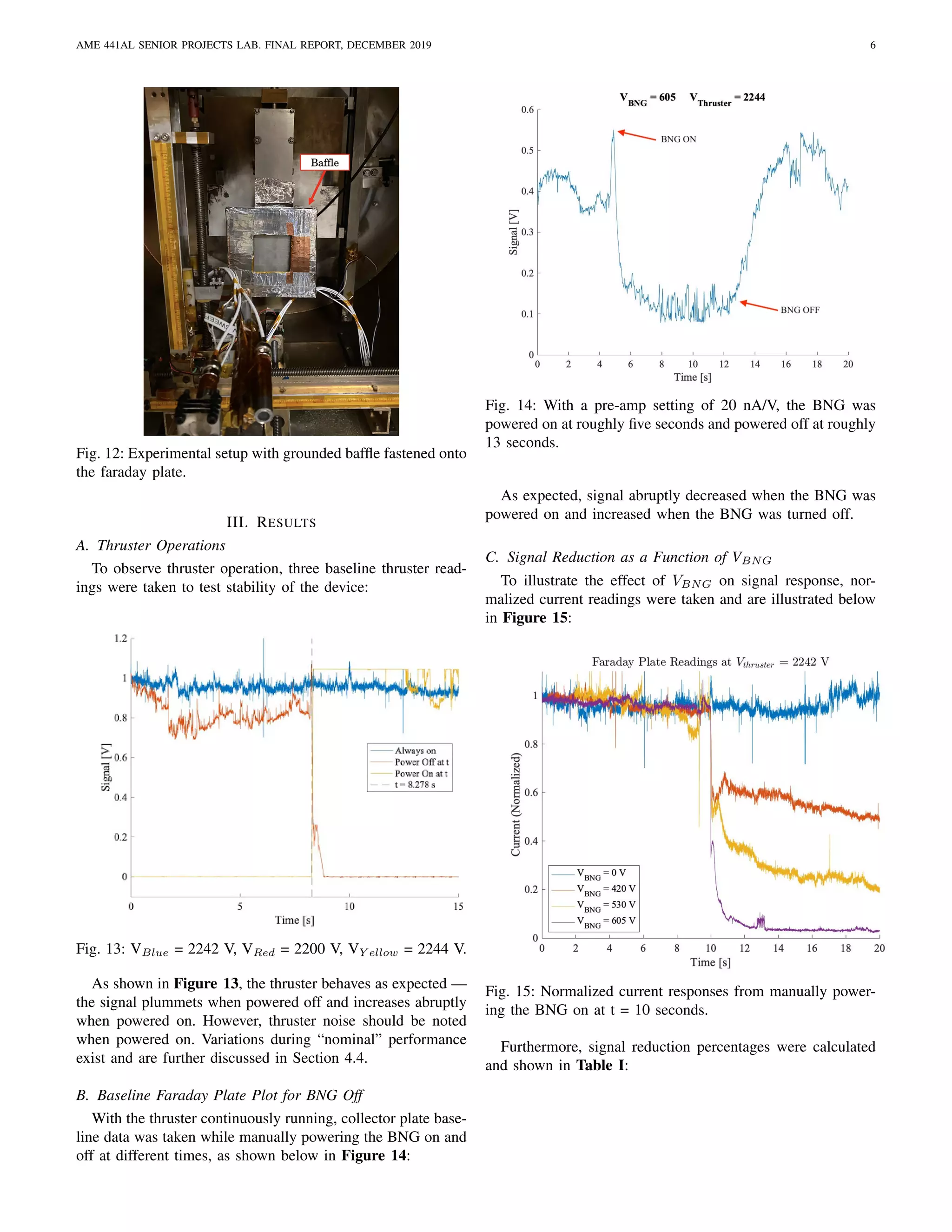
incoming ions [6]. This is shown in Figure 12:
6. AME 441AL SENIOR PROJECTS LAB. FINAL REPORT, DECEMBER 2019 6
Fig. 12: Experimental setup with grounded baffle fastened onto
the faraday plate.
III. RESULTS
A. Thruster Operations
To observe thruster operation, three baseline thruster read-
ings were taken to test stability of the device:
Fig. 13: VBlue = 2242 V, VRed = 2200 V, VY ellow = 2244 V.
As shown in Figure 13, the thruster behaves as expected —
the signal plummets when powered off and increases abruptly
when powered on. However, thruster noise should be noted
when powered on. Variations during “nominal” performance
exist and are further discussed in Section 4.4.
B. Baseline Faraday Plate Plot for BNG Off
With the thruster continuously running, collector plate base-
line data was taken while manually powering the BNG on and
off at different times, as shown below in Figure 14:
Fig. 14: With a pre-amp setting of 20 nA/V, the BNG was
powered on at roughly five seconds and powered off at roughly
13 seconds.
As expected, signal abruptly decreased when the BNG was
powered on and increased when the BNG was turned off.
C. Signal Reduction as a Function of VBNG
To illustrate the effect of VBNG on signal response, nor-
malized current readings were taken and are illustrated below
in Figure 15:
Fig. 15: Normalized current responses from manually power-
ing the BNG on at t = 10 seconds.
Furthermore, signal reduction percentages were calculated
and shown in Table I:
7. AME 441AL SENIOR PROJECTS LAB. FINAL REPORT, DECEMBER 2019 7
TABLE I: Percent signal reduction based on BNG voltage.
V % Reduction
0 0
420 36.8
530 77.2
605 94.0
Unsurprisingly, larger VBNG values correspond to less
captured current, which is due to larger deflection angles.
D. Probe Sweep Results
A theoretical beam deflection angle was calculated at 15.0
±0.2◦
. Using the XYZ stepper motor system, the Faraday
probe was horizontally scanned twice through the ion plume,
and current readings were averaged across both sweeps. With
the thruster centered at 2.125”, current readings over the scan
area are presented in Figure 16:
Fig. 16: Averaged faraday probe scan taken 2.94 ± 0.01” from
the BNG, where VT hruster = 2422 V.
While Figure 16 shows a visible parting of current, the
experimentally calculated deflection angle was just over half
of the theoretical deflection angle, at 8.8 ± 0.2◦
.
E. Theorized Successful TOF
Using Equation 1, theoretical TOF values were calculated
and recorded in Table II for various VT values:
TABLE II: Expected TOF Values for EMI-BF4 Constituents.
V0 1500 [V] 2090 [V] 2244 [V]
Polarity + - + - + -
Monomers* 1.5171 1.3431 1.2852 1.1378 1.2403 1.0981
Dimers* 2.5312 2.4309 2.1444 2.0594 2.0695 1.9875
Trimers* 3.2423 3.1646 2.7468 2.6810 2.6509 2.5874
TOF units are E-5 s.
Theoretical TOF values for VT hruster = 2090 V were
applied to a BNG cycling test, where a positive faraday plate
signal corresponds to the BNG powered on. As the signal
response trends downward, more ions are collected by the
faraday plate. This is due to the signal’s negative polarity,
as shown in Figure 17:
Fig. 17: TOF test results at a cycling frequency of 10 kHz.
IV. DISCUSSION
A. Ion Beam Deflection Angle
Although it is difficult to say with certainty, the 6o
± 2o
error between theoretical and experimental results is likely due
to the thruster’s inconsistent ion flow. Deflection angle equa-
tions assume orthogonal impact, however since the thruster
has a half angle of 36◦
, this assumption was invalid. For that
reason, recorded value of 8.8o
± 0.2o
differs considerably from
the theoretical value of 15.0o
± 0.2o
.
B. Preamplifier Analysis
During initial setup of our TOF data collection system, the
preamplifier was unintentionally exposed to 15 mA of current;
the maximum input current is listed as 10mA. Following
this incident it was discovered that one of the two onboard
op-amps had been damaged and was no longer operational.
For this reason the preamplifier was only able to be used
in gain configurations that used the undamaged op-amp. For
this experiment, the only setting that was available that was
reasonably viable for data collection was a gain setting of 20
nA/V. At this gain setting, the preamplifier output ranged from
0-7 V. At this range our 8-bit VirtualBench was limited to a
less desirable resolution, as can be seen in Figure 17. A lower
gain setting, say 100 nA/V, would have produced a smaller
Vrange and allowed for a higher resolution. Although there
was experimental equipment available with a finer resolution
than the VirtualBench, such as a 16-bit NI-DAQ 6211, this
device did not provide a high enough sampling rate. The NI-
DAQ 6211 is limited to 250 kS/s where the VirtualBench
provides up to 5 MS/s. Due to the high frequency nature
of BNG cycling, the higher sampling frequency is necessary.
Another issue stemming from the preamplifier was the gain
mode setting. There are three gain modes: "Low Noise", "Low
Drift", and "High Bandwidth”, and due to the damaged op-
amp, only the low drift gain mode was available for use. The
low drift setting is a low bandwidth setting that is less capable
of sensing fast changes in input. This is a potential cause for
error due to the high frequency nature of this study.
8. AME 441AL SENIOR PROJECTS LAB. FINAL REPORT, DECEMBER 2019 8
C. Thermal Expansion of Frame
Although Delrin has beneficial properties with respect to
out-gassing and dielectric strength, its relatively high coeffi-
cient of thermal expansion (CTE) proved to be a significant
issue with BNG fabrication, this is demonstrated below in
Figure 18:
Fig. 18: CTE comparison plot of 3 different engineering
plastics.
Due to budget constraints, materials with lower CTE values
could not be obtained. PEEK is a possible substitute for Delrin,
and has a CTE of 2.6E-5. This may avoid thermal expansion
issues (i.e stretching BNG wires past their yield point).
For a BNG epoxied at room temperature then installed in a
cooler vacuum temperature, the frame was “cooled” by 3.8o
C
± 0.5o
C and underwent thermal contraction. This caused the
frame to shrink and wires to slack and arc. The total wire
length of the room temperature BNG was 50.7 ± 0.2 mm
with an average strain of 2.78e-3%.
For the BNG epoxied at a cooler temperature then in-
troduced to a warmer vacuum temperature, the frame was
“heated” by 5.5o
± 0.5o
C and underwent thermal expansion.
In doing so, the frame pulls on the wires and optimizes tension
without surpassing yield strength of 1.8e-4 ± 0.1 MPa. The
total wire length of the chilled BNG was 50.8 ± 0.2 mm with
an average strain of 1.99e-04%.
Delrin’s linear thermal expansion values for room temper-
ature and ice-pack curing temperature are tabulated below,
respectively:
TABLE III: Thermal Expansion Values of the BNG frame and
wires.
Initial T [◦C] Final T [◦C] Frame Wire
(Curing) (Vacuum) Expansion [mm] Expansion [mm]
25.4 ± 0.5 21.6 ± 0.5 -0.231 ± 0.003 -0.141 ± 0.002
16.1 ± 0.5 21.6 ± 0.5 0.334 ± 0.003 0.010 ± 0.002
Figure 19 stress-strain curve undergone by the wires at
chilled (ice) curing temperature, with an elastic limit of 1954.2
MPa and ultimate stress (U) of 2188.7 MPa:
Fig. 19: Stress is proportional to strain, obeying Hooke’s Law.
Here, E is the elastic limit, and U is the ultimate Stress point,
and B is the breaking point [10].
D. Time of Flight
Theoretical TOF values match with the results obtained
in Figure 17, but the accuracy of this data is dubious. The
lack of consistent and reliable TOF values is likely due to
a signal reduction rate of only 77.2% from the 530 V BNG
potential in Figure 15. Because there has yet to be a nearly
100% signal reduction rate, it is unlikely that the faraday plate
(and subsequently the preamplifier) captured such minute,
nanoAmpere changes in signal magnitude. For this reason,
it is more likely that Figure 17 is signal noise rather than
discernable TOF data of the propellant constituents.
Possible explanations for this lack of complete thruster
current reduction, and thus lack of trustworthy TOF tests,
include the following. As the thruster continues to fire in the
vacuum chamber, ambient plasma presence increases, which
may affect faraday plate readings. As shown by the “nominal”
thruster response in Figure 13, there are signal variations on
the order of tenths of volts. Lack of confident TOF tests could
also be attributed to inconsistent thruster responses.
V. CONCLUSION
The goal of this study was to design, construct, and imple-
ment a cost-effective and easily constructed Bradbury-Nielsen
Gate to collect TOF measurements of an electrospray thruster.
To achieve that, it was necessary for the BNG to effectively
deflect the thruster’s ion plume. The BNG constructed for
this study did effectively deflect the ion beam Figure 15.
However, the recorded deflection angle did not meet project
requirements. As discussed in section 4.1, this is likely due to
the falsely assumed orthogonal impact between the ion plume
and the BNG active area.
Lack of appropriate deflection angle compromised validity
and reliability of TOF tests. This failure is not suspected
to be a result of poor bng construction, but rather a result
of several issues in the experimental and data collection
setup. These issues may include fundamental issues between
the faraday plate, preamplifier, Virtual Bench, and LabVIEW
code. Although this was scrutinized and no issues were found,
it remains a possible cause for error.
9. AME 441AL SENIOR PROJECTS LAB. FINAL REPORT, DECEMBER 2019 9
Although the main objective of this study was not achieved,
several useful lessons were learned. The BNG constructed
did meet the project goals of having taut, parallel lines with
uniform 1 mm spacing as shown in Figure 10 and calculated
in Section 1.2. Baffling the faraday plate significantly reduced
system noise, which suggests that a detailed investigation is
required in the experimental set up to further reduce data
uncertainty.
A. Future Work
Future work involves replacing the BNG frame with a
similar material of lower CTE.
In the initial proposal of this project, a scaled 6” x 6”
BNG was suggested. However, due to the myriad problems
described — thermal expansion of the frame, wire deforma-
tion, and the current wire lacing method — the scaled BNG
was not pursued.
To reduce noise of the faraday plate and minimize the
required deflection angle, a more constricting, secured baffle
may be attached to the existing faraday plate.
A more reliable and consistent thruster would eliminate
variants in current, minimize uncertainty and provide refined
data.
In sum, the following must be pursued: a more reliable
experimental set up, fully functioning preamplifier, and a data
acquisition system with higher resolution and sampling rate.
With all these things, BNG cycling tests for TOF can be
repeated, and these changes are expected to enhance reliability
for successfully measuring TOF values.
ACKNOWLEDGMENT
This research was conducted using the facilities of the
USC Laboratory for Advanced Plasma Dynamics (LAPD).
Equipment was supplied in part from funding provided by
the Air Force Research Laboratory (AFRL).
We thank Dr.(s) Matthew Gilpin, Charles Radovich, David
Petty , Rodney Yates, Jeffrey Vargas, William Colvin and the
entire 441a Staff for their assistance with this project.
REFERENCES
[1] Yoon, Oh Kyu, et al. “Simple Template-Based Method to Pro-
duce BradburyNielsen Gates.” Journal of the American Society
for Mass Spectrometry, vol. 18, no. 11, 2007, pp. 1901–1908.,
doi:10.1016/j.jasms.2007.07.030.
[2] R. H. Price and R. P. Phillips, “The force between two charged wires,”
American Journal of Physics, vol. 58, no. 6, pp. 534–539, 1990.
[3] Cravath, A. M. The Rate of Formation of Negative Ions by Electron
Attachment. Phys. Rev. 1929, 33, 605–613.
[4] Weinkauf, R.; Walter, K.; Weickhart, C.; Boesl, U.; Schlag, E. W. Laser
Tandem Mass Spectrometry in a Time of Flight Instrument. Naturforsch
Teil A 1989, 44, 1219–1225.
[5] Kimmel, Joel R, et al. “Novel Method for the Production of Finely
Spaced Bradbury-Nielson Gates.” Review of Scientific Instruments, vol.
72, no. 12, 27 Aug. 2001, doi:10.1063/1.1416109.
[6] Interview with Robert Antypas. September 3, 2019.
[7] DU Pont, Delrin Acetal Resin, Design Guide – Module III
[8] Anon, et al. “Smallest Gradient Along Contour Lines” August, 2015.
[9] Courtney, Daniel G., et al. “Comparing Direct and Indirect Thrust
Measurements from Passively Fed Ionic Electrospray Thrusters.” Jour-
nal of Propulsion and Power, vol. 32, no. 2, 2016, pp. 392–407.,
doi:10.2514/1.b35836
[10] Jalal Afsa. “Stress Strain Curve Explanation”. September 14, 2014
[11] Brunner, T., et al. “A Large Bradbury Nielsen Ion Gate with Flexible
Wire Spacing Based on Photo-Etched Stainless Steel Grids and Its
Characterization Applying Symmetric and Asymmetric Potentials.” In-
ternational Journal of Mass Spectrometry, vol. 309, 2012, pp. 97–103.,
doi:10.1016/j.ijms.2011.09.004.
[12] Bandhauer, Lorien, et al. Design and Construction of a Bradbury-
Nielsen Gate for Determining the Time of Flight of an Electrospray
Propulsion System. 2018, Design and Construction of a Bradbury-
Nielsen Gate for Determining the Time of Flight of an Electrospray
Propulsion System. Senior Design Project Proposal.
[13] Verbeck, G. F.; Saini, R.; Wylde, J.; Tsui, K., Ellis, M. MEMS
Assembled Mass Spectrometry: A Novel Approach to Miniaturization
and Construction of Electron and Ion Optics. Proceedings of the 54th
ASMS Conference on Mass Spectrometry; Seattle, WA, May 28–June
1, 2006.
[14] Szumlas, Andrew W., et al. “Design and Construction of a Me-
chanically Simple, Interdigitated-Wire Ion Gate.” Review of Sci-
entific Instruments, vol. 76, no. 8, 12 Aug. 2005, p. 086108.,
doi:10.1063/1.2006308.