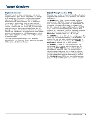
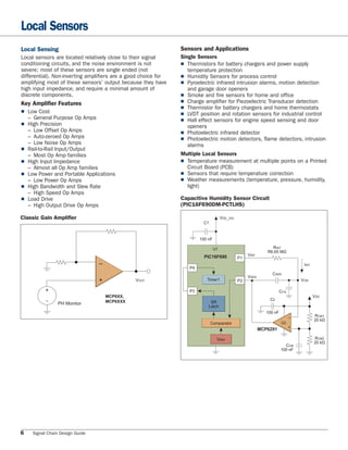
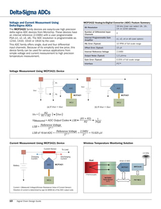
The document provides an overview of devices that can be used in sensor signal chains, including operational amplifiers, comparators, analog-to-digital converters, temperature sensors, voltage references, digital potentiometers, and digital-to-analog converters. It describes a typical sensor signal chain involving analog and digital domains, with sensors outputting low-level analog signals that are amplified, filtered, and converted to digital for processing by a microcontroller. The document lists common sensor types and phenomena they measure, like temperature, humidity, pressure, and their typical electrical outputs.

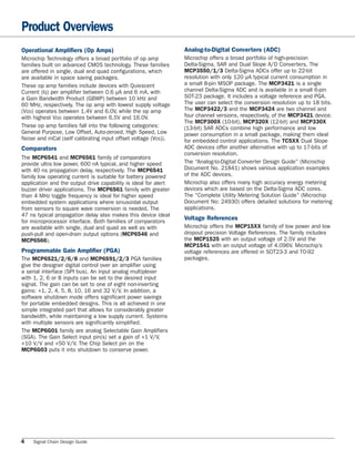
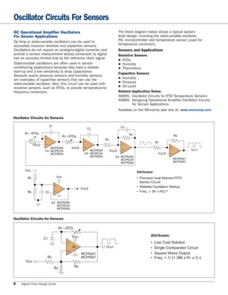
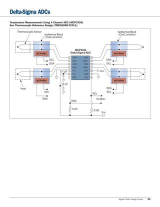
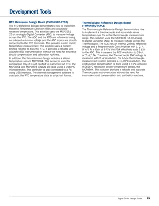
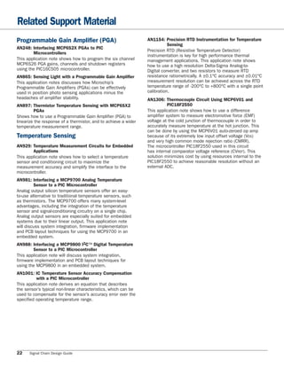
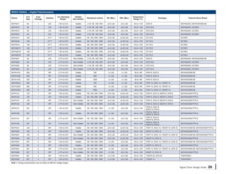
![Wheatstone Bridge
Bridge Sensor Circuit steps (if any) should be used to increase the overall system
Sensors for temperature, pressure, load or other phys- resolution when using the MCP355X. In many situations, the
ical excitation quantities are most often configured in a MCP355X devices can be used to directly digitize the sensor
Wheatstone bridge configuration. The bridge can have output, eliminating any need for external signal conditioning
anywhere from one to all four elements reacting to the circuitry.
physical excitation, and should be used in a ratiometeric Using the absolute pressure sensor as our Wheatstone
configuration when possible, with the system reference bridge example, the NPP-301 device has a typical full
driving both the sensor and the ADC voltage reference. By scale output of 60 mV when excited with a 3V battery. The
using the same reference for both the sensor excitation and pressure range for this device is 100 kPa. The MCP3551
ADC, the variation in the reference can be cancelled out. has a output noise specification of 2.5 μVRMS.
Furthermore, the output voltage from the bridge sensor is The following equation is a first order approximation of the
proportional to the excitation voltage. Therefore, the ADC relationship between pressure in pascals (P) and altitude (h),
that is using the external reference is more popular than in meters.
the ADC that is using internal reference, for the ratiometric h
configuration. log(P) ≈ 5 –
15500
One example sensor from GE NovaSensor is an absolute
Using 60 mV as the full scale range and 2.5 μV as the
pressure sensor, shown below, a four element varying
resolution, the resulting resolution from direct digitization in
bridge. This example uses the MCP355X family of delta
meters is 0.64 meters or approximately 2 feet.
sigma ADCs. When designing with the MCP355X family
of 22-bit delta-sigma ADCs, the initial step should be to It should be noted that this is only used as an example for
evaluate the sensor performance and then determine what discussion; temperature effects and the error from a first
order approximation must be included in final system design.
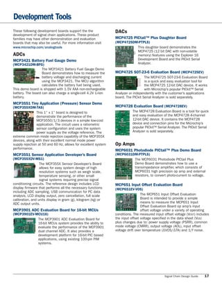
Example of Wheatstone Bridge Sensor Configuration with High Resolution Delta-Sigma ADC
0.1 μF 1.0 μF
To VDD
NPP-301
1 8
2 VDD
VREF
R2 VIN+
SCK SPI
MCP3551 SDO MCU
R1 R3
VIN- CS 5, 6, 7
3 VSS
4
R4
Altimeter Watch
∆V ~ [(∆R2+ ∆R4) - (∆R1+∆R3)]/4R * VDD
With R1 = R2 = R3 = R4 = R
Signal Chain Design Guide 9](https://image.slidesharecdn.com/21825f-120829120726-phpapp01/85/great-adc-9-320.jpg)


![A3918 low voltage dc motor driver allegro datasheet[1]](https://cdn.slidesharecdn.com/ss_thumbnails/a3918lowvoltagedcmotordriverallegro-datasheet1-121031142106-phpapp01-thumbnail.jpg?width=640&height=640&fit=bounds)


