Input Output Organization
I/OSubsystem
• Provides an efficient mode of communication between the central
system and the outside environment.
• Programs and data must be entered into computer memory for
processing and results obtained from computer must be recorded
and displayed to user
4.
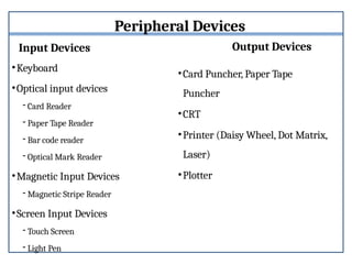
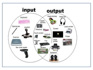
Peripheral Devices
• Devicesthat are under direct control of computer are said to be
connected on-line.
• Input or output devices attached to the computer are also called
peripherals.
• There are three types of peripherals :
• Input peripherals
• Output peripherals
• Input-output peripherals
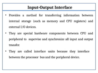
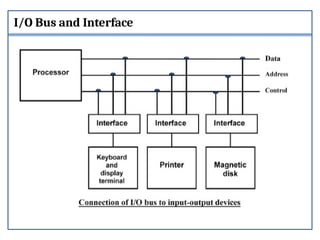
Input-Output Interface
• Providesa method for transferring information between
internal storage (such as memory and CPU registers) and
external I/O devices.
• They are special hardware components between CPU and
peripheral to supervise and synchronize all input and output
transfer.
• They are called interface units because they interface
between the processor bus and the peripheral device.
8.
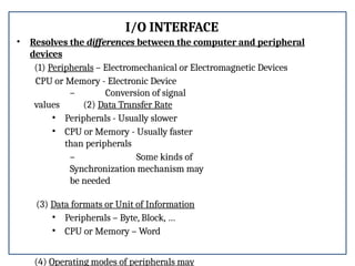
I/O INTERFACE
• Resolvesthe differences between the computer and peripheral
devices
(1) Peripherals – Electromechanical or Electromagnetic Devices
CPU or Memory - Electronic Device
– Conversion of signal
values (2) Data Transfer Rate
• Peripherals - Usually slower
• CPU or Memory - Usually faster
than peripherals
– Some kinds of
Synchronization mechanism may
be needed
(3) Data formats or Unit of Information
• Peripherals – Byte, Block, …
• CPU or Memory – Word
(4) Operating modes of peripherals may
Interface
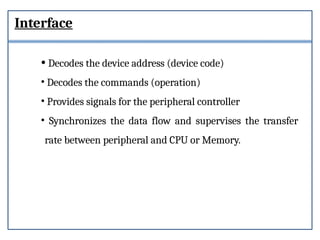
• Decodes thedevice address (device code)
• Decodes the commands (operation)
• Provides signals for the peripheral controller
• Synchronizes the data flow and supervises the transfer
rate between peripheral and CPU or Memory.
11.
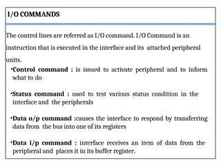
•Control command :is issued to activate peripheral and to inform
what to do
•Status command : used to test various status condition in the
interface and the peripherals
•Data o/p command :causes the interface to respond by transferring
data from the bus into one of its registers
•Data i/p command : interface receives an item of data from the
peripheral and places it in its buffer register.
The control lines are referred as I/O command. I/O Command is an
instruction that is executed in the interface and its attached peripheral
units.
I/O COMMANDS
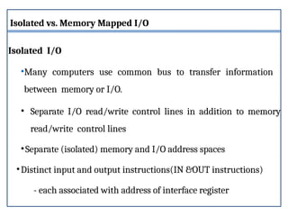
Isolated vs. MemoryMapped I/O
Isolated I/O
•Many computers use common bus to transfer information
between memory or I/O.
• Separate I/O read/write control lines in addition to memory
read/write control lines
•Separate (isolated) memory and I/O address spaces
•Distinct input and output instructions(IN &OUT instructions)
- each associated with address of interface register
14.
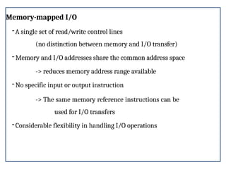
Memory-mapped I/O
-A singleset of read/write control lines
(no distinction between memory and I/O transfer)
- Memory and I/O addresses share the common address space
-> reduces memory address range available
- No specific input or output instruction
-> The same memory reference instructions can be
used for I/O transfers
- Considerable flexibility in handling I/O operations
15.
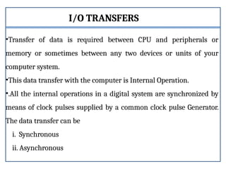
I/O TRANSFERS
•Transfer ofdata is required between CPU and peripherals or
memory or sometimes between any two devices or units of your
computer system.
•This data transfer with the computer is Internal Operation.
•.All the internal operations in a digital system are synchronized by
means of clock pulses supplied by a common clock pulse Generator.
The data transfer can be
i. Synchronous
ii. Asynchronous
16.
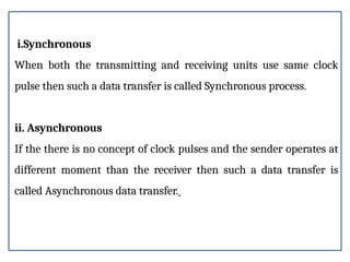
i.Synchronous
When both thetransmitting and receiving units use same clock
pulse then such a data transfer is called Synchronous process.
ii. Asynchronous
If the there is no concept of clock pulses and the sender operates at
different moment than the receiver then such a data transfer is
called Asynchronous data transfer.
17.
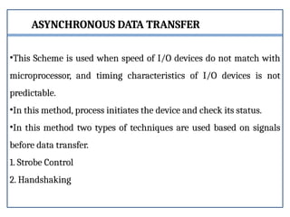
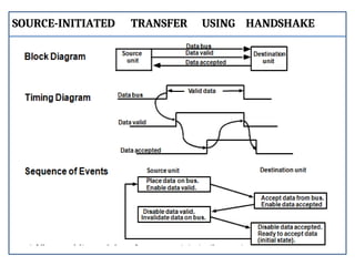
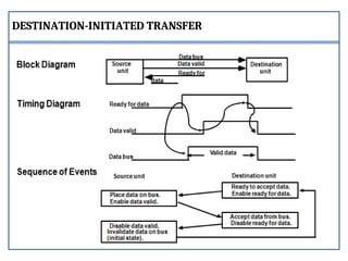
ASYNCHRONOUS DATA TRANSFER
•ThisScheme is used when speed of I/O devices do not match with
microprocessor, and timing characteristics of I/O devices is not
predictable.
•In this method, process initiates the device and check its status.
•In this method two types of techniques are used based on signals
before data transfer.
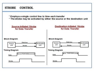
1. Strobe Control
2. Handshaking
Problems in StrobeControl
Source-Initiated
The source unit that initiates the transfer has no way of knowing
whether the destination unit has actually received data.
Destination-Initiated
The destination unit that initiates the transfer no way of knowing
whether the source has actually placed the data on the bus.
20.
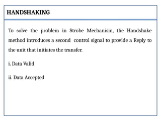
To solve theproblem in Strobe Mechanism, the Handshake
method introduces a second control signal to provide a Reply to
the unit that initiates the transfer.
i. Data Valid
ii. Data Accepted
HANDSHAKING
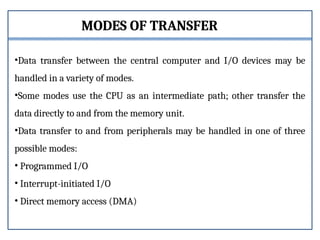
MODES OF TRANSFER
•Datatransfer between the central computer and I/O devices may be
handled in a variety of modes.
•Some modes use the CPU as an intermediate path; other transfer the
data directly to and from the memory unit.
•Data transfer to and from peripherals may be handled in one of three
possible modes:
• Programmed I/O
• Interrupt-initiated I/O
• Direct memory access (DMA)
24.
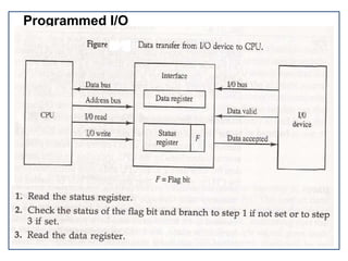
Programmed I/O
•Programmed I/Ooperations are the result of I/O instructions
written in the computer program.
•Each data item transfer is initiated by an instruction in the
program.
•Transferring data under program control requires constant
monitoring of the peripheral by the CPU.
•Once a data transfer is initiated, the CPU is required to monitor the
interface to see when a transfer can again be made.
• It is up to the programmed instructions executed in the CPU.
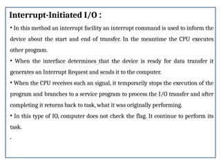
Interrupt-Initiated I/O :
•In this method an interrupt facility an interrupt command is used to inform the
device about the start and end of transfer. In the meantime the CPU executes
other program.
• When the interface determines that the device is ready for data transfer it
generates an Interrupt Request and sends it to the computer.
• When the CPU receives such an signal, it temporarily stops the execution of the
program and branches to a service program to process the I/O transfer and after
completing it returns back to task, what it was originally performing.
• In this type of IO, computer does not check the flag. It continue to perform its
task.
.
27.
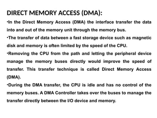
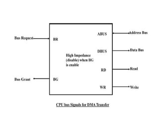
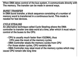
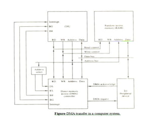
DIRECT MEMORY ACCESS(DMA):
•In the Direct Memory Access (DMA) the interface transfer the data
into and out of the memory unit through the memory bus.
•The transfer of data between a fast storage device such as magnetic
disk and memory is often limited by the speed of the CPU.
•Removing the CPU from the path and letting the peripheral device
manage the memory buses directly would improve the speed of
transfer. This transfer technique is called Direct Memory Access
(DMA).
•During the DMA transfer, the CPU is idle and has no control of the
memory buses. A DMA Controller takes over the buses to manage the
transfer directly between the I/O device and memory.
28.
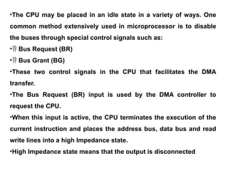
•The CPU maybe placed in an idle state in a variety of ways. One
common method extensively used in microprocessor is to disable
the buses through special control signals such as:
• Bus Request (BR)
• Bus Grant (BG)
•These two control signals in the CPU that facilitates the DMA
transfer.
•The Bus Request (BR) input is used by the DMA controller to
request the CPU.
•When this input is active, the CPU terminates the execution of the
current instruction and places the address bus, data bus and read
write lines into a high Impedance state.
•High Impedance state means that the output is disconnected
31.
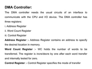
DMA Controller:
The DMAcontroller needs the usual circuits of an interface to
communicate with the CPU and I/O device. The DMA controller has
three registers:
i. Address Register
ii. Word Count Register
iii. Control Register
Address Register :- Address Register contains an address to specify
the desired location in memory.
Word Count Register :- WC holds the number of words to be
transferred. The register is incre/decre by one after each word transfer
and internally tested for zero.
Control Register :- Control Register specifies the mode of transfer
33.
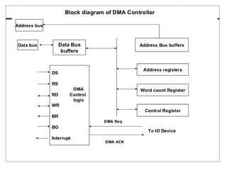
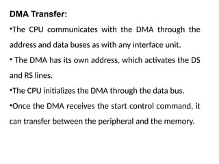
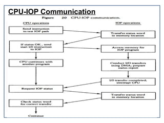
DMA Transfer:
•The CPUcommunicates with the DMA through the
address and data buses as with any interface unit.
• The DMA has its own address, which activates the DS
and RS lines.
•The CPU initializes the DMA through the data bus.
•Once the DMA receives the start control command, it
can transfer between the peripheral and the memory.
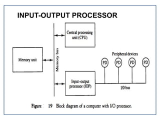
• The blockdiagram of a computer along with various I/O
Processors.
• The memory unit occupies the central position and can
communicate with each processor.
• The CPU processes the data required for solving the
computational tasks.
• The IOP provides a path for transfer of data between
peripherals and memory.
• The CPU assigns the task of initiating the I/O program.
• The IOP operates independent from CPU and transfer data
between peripherals and memory.
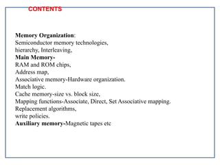
CONTENTS
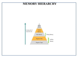
Memory Organization:
Semiconductor memorytechnologies,
hierarchy, Interleaving,
Main Memory-
RAM and ROM chips,
Address map,
Associative memory-Hardware organization.
Match logic.
Cache memory-size vs. block size,
Mapping functions-Associate, Direct, Set Associative mapping.
Replacement algorithms,
write policies.
Auxiliary memory-Magnetic tapes etc
40.
Memory is usedfor storing programs and data that are required
to perform a specific task.
For CPU to operate at its maximum speed, it required an
uninterrupted and high speed access to these memories that
contain programs and data. Some of the criteria need to be taken
into consideration while deciding which memory is to be used:
• Cost
• Speed
• Memory access time
• Data transfer rate
• Reliability
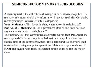
SEMICONDUCTOR MEMORY TECHNOLOGIES
Amemory unit is the collection of storage units or devices together. The
memory unit stores the binary information in the form of bits. Generally,
memory/storage is classified into 2 categories:
Volatile Memory: This loses its data, when power is switched off.
Non-Volatile Memory: This is a permanent storage and does not lose
any data when power is switched off.
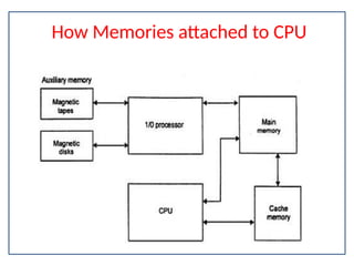
The memory unit that communicates directly within the CPU, Auxillary
memory and Cache memory, is called main memory. It is the central
storage unit of the computer system. It is a large and fast memory used
to store data during computer operations. Main memory is made up of
RAM and ROM, with RAM integrated circuit chips holing the major
share.
43.
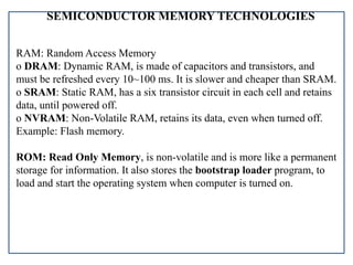
SEMICONDUCTOR MEMORY TECHNOLOGIES
RAM:Random Access Memory
o DRAM: Dynamic RAM, is made of capacitors and transistors, and
must be refreshed every 10~100 ms. It is slower and cheaper than SRAM.
o SRAM: Static RAM, has a six transistor circuit in each cell and retains
data, until powered off.
o NVRAM: Non-Volatile RAM, retains its data, even when turned off.
Example: Flash memory.
ROM: Read Only Memory, is non-volatile and is more like a permanent
storage for information. It also stores the bootstrap loader program, to
load and start the operating system when computer is turned on.
44.
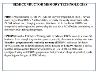
SEMICONDUCTOR MEMORY TECHNOLOGIES
PROM(ProgrammableROM)- PROMs can only be programmed once. They are
more fragile than ROMs. A jolt of static electricity can easily cause fuses in the
PROM to burn out, changing essential bits from 1 to 0. But blank PROMs are
inexpensive and are great for prototyping the data for a ROM before committing to
the costly ROM fabrication process.
EPROM(Erasable PROM) :- Working with ROMs and PROMs can be a wasteful
business. Even though they are inexpensive per chip, the cost can add up over time.
Erasable programmable read-only memory (EPROM) addresses this issue.
EPROM chips can be rewritten many times. Erasing an EPROM requires a special
tool that emits a certain frequency of ultraviolet (UV) light. EPROMs are
configured using an EPROM programmer that provides voltage at specified levels
depending on the type of EPROM used
45.
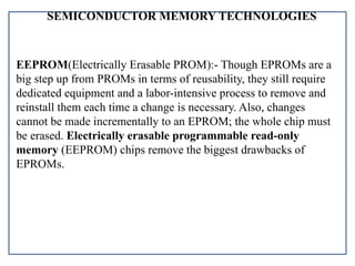
SEMICONDUCTOR MEMORY TECHNOLOGIES
EEPROM(ElectricallyErasable PROM):- Though EPROMs are a
big step up from PROMs in terms of reusability, they still require
dedicated equipment and a labor-intensive process to remove and
reinstall them each time a change is necessary. Also, changes
cannot be made incrementally to an EPROM; the whole chip must
be erased. Electrically erasable programmable read-only
memory (EEPROM) chips remove the biggest drawbacks of
EPROMs.
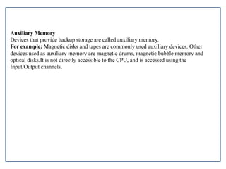
Auxiliary Memory
Devices thatprovide backup storage are called auxiliary memory.
For example: Magnetic disks and tapes are commonly used auxiliary devices. Other
devices used as auxiliary memory are magnetic drums, magnetic bubble memory and
optical disks.It is not directly accessible to the CPU, and is accessed using the
Input/Output channels.
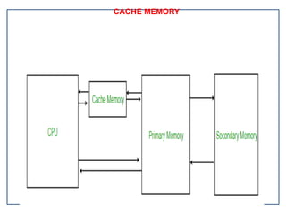
CACHE MEMORY
Cache Memoryis a special very high-speed memory. It is used to speed up and
synchronizing with high-speed CPU.
Cache memory is costlier than main memory or disk memory but economical than
CPU registers.
Cache memory is an extremely fast memory type that acts as a buffer between RAM
and the CPU. It holds frequently requested data and instructions so that they are
immediately available to the CPU when needed.
Cache memory is used to reduce the average time to access data from the Main
memory.
The cache is a smaller and faster memory which stores copies of the data from
frequently used main memory locations.
There are various different independent caches in a CPU, which store instructions
and data.
50.
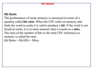
HIT RATIO
Hit Ratio
Theperformance of cache memory is measured in terms of a
quantity called hit ratio. When the CPU refers to memory and
finds the word in cache it is said to produce a hit. If the word is not
found in cache, it is in main memory then it counts as a miss.
The ratio of the number of hits to the total CPU references to
memory is called hit ratio.
Hit Ratio = Hit/(Hit + Miss)
51.
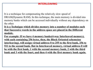
INTERLEAVING
It is atechnique for compensating the relatively slow speed of
DRAM(Dynamic RAM). In this technique, the main memory is divided into
memory banks which can be accessed individually without any dependency on
the other.
It is a Technique which divides memory into a number of modules such
that Successive words in the address space are placed in the Different
module.
For example: If we have 4 memory banks(4-way Interleaved memory),
with each containing 256 bytes, then, the Block Oriented scheme(no
interleaving), will assign virtual address 0 to 255 to the first bank, 256 to
511 to the second bank. But in Interleaved memory, virtual address 0 will
be with the first bank, 1 with the second memory bank, 2 with the third
bank and 3 with the fourt, and then 4 with the first memory bank again.
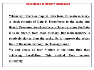
Advantages of Memoryinterleaving
Whenever, Processor request Data from the main memory.
A block (chunk) of Data is Transferred to the cache and
then to Processor. So whenever a cache miss occurs the Data
is to be fetched from main memory. But main memory is
relatively slower than the cache. So to improve the access
time of the main memory interleaving is used.
We can access all four Module at the same time thus
achieving Parallelism. This method Uses memory
effectively.
54.
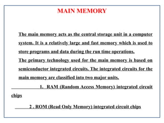
MAIN MEMORY
The mainmemory acts as the central storage unit in a computer
system. It is a relatively large and fast memory which is used to
store programs and data during the run time operations.
The primary technology used for the main memory is based on
semiconductor integrated circuits. The integrated circuits for the
main memory are classified into two major units.
1. RAM (Random Access Memory) integrated circuit
chips
2 . ROM (Read Only Memory) integrated circuit chips
55.
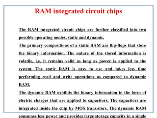
RAM integrated circuitchips
The RAM integrated circuit chips are further classified into two
possible operating modes, static and dynamic.
The primary compositions of a static RAM are flip-flops that store
the binary information. The nature of the stored information is
volatile, i.e. it remains valid as long as power is applied to the
system. The static RAM is easy to use and takes less time
performing read and write operations as compared to dynamic
RAM.
The dynamic RAM exhibits the binary information in the form of
electric charges that are applied to capacitors. The capacitors are
integrated inside the chip by MOS transistors. The dynamic RAM
consumes less power and provides large storage capacity in a single
56.
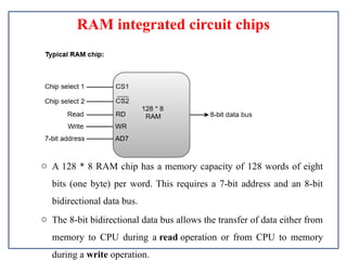
RAM integrated circuitchips
o A 128 * 8 RAM chip has a memory capacity of 128 words of eight
bits (one byte) per word. This requires a 7-bit address and an 8-bit
bidirectional data bus.
o The 8-bit bidirectional data bus allows the transfer of data either from
memory to CPU during a read operation or from CPU to memory
during a write operation.
57.
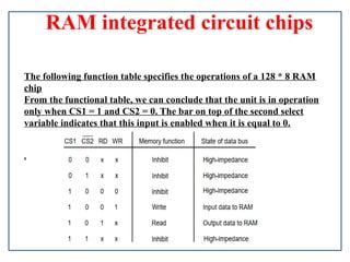
RAM integrated circuitchips
The following function table specifies the operations of a 128 * 8 RAM
chip
From the functional table, we can conclude that the unit is in operation
only when CS1 = 1 and CS2 = 0. The bar on top of the second select
variable indicates that this input is enabled when it is equal to 0.
.
58.
ROM integrated circuit
Theprimary component of the main memory is RAM integrated
circuit chips, but a portion of memory may be constructed with
ROM chips.A ROM memory is used for keeping programs and data
that are permanently resident in the computer.
Apart from the permanent storage of data, the ROM portion of
main memory is needed for storing an initial program called
a bootstrap loader. The primary function of the bootstrap
loader program is to start the computer software operating when
power is turned on.
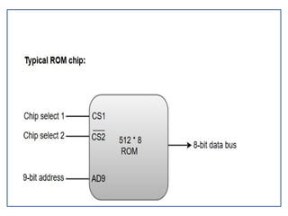
ROM chips are also available in a variety of sizes and are also used
as per the system requirement. The following block diagram
demonstrates the chip interconnection in a 512 * 8 ROM chip.
60.
MEMORY ADDRESS MAP
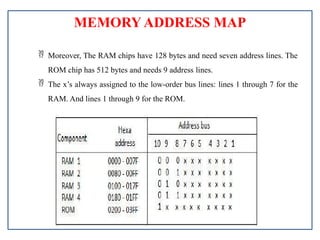
Moreover, The RAM chips have 128 bytes and need seven address lines. The
ROM chip has 512 bytes and needs 9 address lines.
The x’s always assigned to the low-order bus lines: lines 1 through 7 for the
RAM. And lines 1 through 9 for the ROM.
61.
MEMORY ADDRESS MAP
The x’s always assigned to the low-order bus lines: lines 1 through 7 for the
RAM. And lines 1 through 9 for the ROM.
It is now necessary to distinguish between four RAM chips by assigning to each a
different address. For this particular example, we choose bus lines 8 and 9 to
represent four distinct binary combinations.
Also, The table clearly shows that the nine low-order bus lines constitute a
memory space for RAM equal to 29 = 512 bytes.
The distinction between a RAM and ROM address done with another bus line.
Here we choose line 10 for this purpose.
When line 10 0, the CPU selects a RAM, and when this line equal to 1, it selects
the ROM.