The document describes a proposed photovoltaic-grid integrated system that directly energizes AC loads from a solar array during the daytime using a variable voltage tracking system (VVT). The VVT aims to maintain the average output chopped voltage at a fixed value regardless of solar radiation levels. This is achieved by integrating a complementary buck-boost chopper and a DC to AC converter. The grid contributes power when there is insufficient power from the solar array due to low irradiation or at night. Matlab/Simulink is used to simulate the proposed model and confirm the approach.
![2012 First International Conference on Renewable Energies and Vehicular Technology
PHOTOVOLTAIC-GRID INTEGRATED SYSTEM
Sameer Khader, Abdel-Karim Daud
Palestine Polytechnic University
emails: Sameer@ppu.edu, daud@ppu.edu
ABSTRACT at realizing the required voltage level during different
periods of day for certain application type such as
This paper proposed solution for directly energizing pumps, motors in general and power supplies.
of ac load throughout Photovoltaic Solar Array during During the design process of PV array powered
the daytime by applying so called variable voltage systems; a simulation must be performed for system
tracking system (VVT). The main function of VVT is analysis and parameter settings. Therefore an efficient
to maintain the average output chopped voltage at fixed user friendly simulation model of the PV array with
value irrespective of solar radiation rate, in turn the various control strategies is always needed.
chopped voltage is converted into ac voltage suitable The proposed model consists of several modules as
for grid-connected loads. This solution is realized by shown in Figure1 with the following functions:
integrating both complementary buck-boost chopper - PV Photovoltaic Module (PV) that converts the
and dc to ac converter. The ac-grid contributes to the solar irradiation into voltage Vpv and current Ipv.
load in two cases, first when there is a power shortage
during the daytime due to weak irradiation rates, and - Complementary Buck-Boost DC Chopper Module
second during the night time. The power estimator unit that boosts up the PV voltage to the predetermined
is used to determine the grid contribution intervals. levels. Conversely in case of high Vpv the output
This solution excludes the use of battery bank voltage is reduced.
which is the main obstacle in massive use of solar Variable
energy due to their weight, short life time, maintenance Voltage
and cost. Matlab/Simulink is used to simulate the Vg_Q Tracking
proposed model, where the obtained simulation results
confirm and justify the proposed approach for further Vout
Vref
study and looking for optimized solutions for cost PV Complement-
Array ary Buck-Boost
reduction and energy savings.
Grid
Index Terms-- Photovoltaic Systems, DC Choppers, Vg_sl Selector Inverter
Smart Grids, Soft Switching, Inverters, Buck-Boost
Chopper. Vac
AC Grid Adapting
Grid System
1. INTRODUCTION Load
Grid-Drop Iout
Photovoltaic energy resources presents alternative Compensation
and friendly to the environment sources. It presents
unique solution for providing remote area with clean Pac
Power Status
and sustainable energy during the daytime in heating, Ppv Estimator
lighting, refrigeration and water pumps systems [1-3]
without the need of battery system, while during the
Figure 1. PV-Grid system block diagram
night time the accumulated energy can be fully or
partially used to cover the energy domain.
The output circuit connected to the photovoltaic - Variable Voltage Tracking Module that generates
system is usually dc-dc converters mainly boost switching pulses according to the required output
choppers in order to boost the voltage to the voltage level in order to maintain Vout at fixed value.
predetermined levels. - Grid Adapting Module that converts the ac grid
The DC/DC converters are widely used in regulated voltage into dc voltage in case of grid connection.
switch mode power supplies, where the input voltage to - Grid Drop Compensation Module that compensates
these converters varies in wide range especially in the the voltage drop according to the drawn load current
case of photovoltaic (PV) supply source due to and generates reference voltage.
unpredictable and sudden change in the solar - Power-Status Estimator that detects the available
irradiation level as well as the cell operating Ppv power, the consumed load power and the value of
temperature. Several connection topologies concerning
power shortage that should be supplied from AC-grid.
the switching systems have been proposed [4-8] aiming
978-1-4673-1170-0/12/$31.00 ©2012 IEEE 60](https://image.slidesharecdn.com/cmp0200-ieee-130115020213-phpapp02/85/Cmp0200-ieee-1-320.jpg)
![2012 First International Conference on Renewable Energies and Vehicular Technology
PHOTOVOLTAIC-GRID INTEGRATED SYSTEM
Sameer Khader, Abdel-Karim Daud
Palestine Polytechnic University
emails: Sameer@ppu.edu, daud@ppu.edu
ABSTRACT at realizing the required voltage level during different
periods of day for certain application type such as
This paper proposed solution for directly energizing pumps, motors in general and power supplies.
of ac load throughout Photovoltaic Solar Array during During the design process of PV array powered
the daytime by applying so called variable voltage systems; a simulation must be performed for system
tracking system (VVT). The main function of VVT is analysis and parameter settings. Therefore an efficient
to maintain the average output chopped voltage at fixed user friendly simulation model of the PV array with
value irrespective of solar radiation rate, in turn the various control strategies is always needed.
chopped voltage is converted into ac voltage suitable The proposed model consists of several modules as
for grid-connected loads. This solution is realized by shown in Figure1 with the following functions:
integrating both complementary buck-boost chopper - PV Photovoltaic Module (PV) that converts the
and dc to ac converter. The ac-grid contributes to the solar irradiation into voltage Vpv and current Ipv.
load in two cases, first when there is a power shortage
during the daytime due to weak irradiation rates, and - Complementary Buck-Boost DC Chopper Module
second during the night time. The power estimator unit that boosts up the PV voltage to the predetermined
is used to determine the grid contribution intervals. levels. Conversely in case of high Vpv the output
This solution excludes the use of battery bank voltage is reduced.
which is the main obstacle in massive use of solar Variable
energy due to their weight, short life time, maintenance Voltage
and cost. Matlab/Simulink is used to simulate the Vg_Q Tracking
proposed model, where the obtained simulation results
confirm and justify the proposed approach for further Vout
Vref
study and looking for optimized solutions for cost PV Complement-
Array ary Buck-Boost
reduction and energy savings.
Grid
Index Terms-- Photovoltaic Systems, DC Choppers, Vg_sl Selector Inverter
Smart Grids, Soft Switching, Inverters, Buck-Boost
Chopper. Vac
AC Grid Adapting
Grid System
1. INTRODUCTION Load
Grid-Drop Iout
Photovoltaic energy resources presents alternative Compensation
and friendly to the environment sources. It presents
unique solution for providing remote area with clean Pac
Power Status
and sustainable energy during the daytime in heating, Ppv Estimator
lighting, refrigeration and water pumps systems [1-3]
without the need of battery system, while during the
Figure 1. PV-Grid system block diagram
night time the accumulated energy can be fully or
partially used to cover the energy domain.
The output circuit connected to the photovoltaic - Variable Voltage Tracking Module that generates
system is usually dc-dc converters mainly boost switching pulses according to the required output
choppers in order to boost the voltage to the voltage level in order to maintain Vout at fixed value.
predetermined levels. - Grid Adapting Module that converts the ac grid
The DC/DC converters are widely used in regulated voltage into dc voltage in case of grid connection.
switch mode power supplies, where the input voltage to - Grid Drop Compensation Module that compensates
these converters varies in wide range especially in the the voltage drop according to the drawn load current
case of photovoltaic (PV) supply source due to and generates reference voltage.
unpredictable and sudden change in the solar - Power-Status Estimator that detects the available
irradiation level as well as the cell operating Ppv power, the consumed load power and the value of
temperature. Several connection topologies concerning
power shortage that should be supplied from AC-grid.
the switching systems have been proposed [4-8] aiming
978-1-4673-1170-0/12/$31.00 ©2012 IEEE 60](https://image.slidesharecdn.com/cmp0200-ieee-130115020213-phpapp02/75/Cmp0200-ieee-1-2048.jpg)
![The displyed in fig.1 parameters Ppv, Vac, Pac, Iout boosting up the output voltage to predetermined value
are PV power, AC-grid voltage and power, and load it is necessary to illustrate the obtained PV voltage and
current respectively; Vgsl, Vref and Vgo are grid selector current for boost chopper according to specifications
signal, reference voltage and complementary buck- given in table 1 at reference irradiation 1000W/m2.
boost driving signals.
The remainder of the paper is organized as follows: Table 1: Data specification for PV Array.
Section (2) Modelling & simulation of PV array; q K Iph Id RS RP TC
Section (3) The behaviours of PV-Grid integrated 1.602e- 1.38e-
system; Section (4) Discusses the simulation results 4A 0.2mA 1mΩ 10kΩ 25°C
19 C 23J/°K
and conclusion. NS NP VO VOC ISC VMPP IMPP
38 4 0.6V 21.5 V 4A 17.5V 3.7A
2. MODELING OF PV ARRAY NSm NPm Vpv out Rload
6 1 130V 44Ω
2.1 Characteristics of PV Array
The PV Array voltage can be obtained by
Basically, PV cell is a P-N semiconductor junction that multiplying the module voltage and current by Nsm and
directly converts light energy into electricity. It has the Npm that represents number of series and parallel
equivalent circuit shown in Figure 2 [8-10]. connected modules respectively.
Continuous
powergui G_T
1 11 .2903 T +
- v
T T_var
V2
Figure 2. Equivalent circuit for PV cell G_var2
G
Where Iph represents the cell photocurrent; Rp and i
Lo Output
6 Ns +Vpv + -
Rs are the intrinsic shunt and series resistance of the Nsm I
cell respectively; Id is the diode saturation current; Vo 1 Np
and Io are the cell output voltage and current Npm +
v
R-L -
respectively. The following are the simplified equations GND
V1
Rf-Cf
describing the cell output voltage and current: PV Array
A.K.Tc ⎛ Iph + Id − Io ⎞
Vo = ln ⎜ ⎟ − R s.Io (1)
q ⎝ Io ⎠
⎛ qAVo ./Tc
. Ns
⎞ a) Proposed model for PV Array in simulink
⎜ e .K
Io = N p ( Iph − Id ⎜ − 1⎟ (2) environment
⎟
⎝ ⎠ 5
I-V performance
4.5 1200W/m2
3 q . Eg ⎛ 1 1 ⎞
⎛ Tc ⎞
4
⎜ − ⎟ 1000W/m2
I d = I or ⎜ ⎟ .e
B . K ⎝ Tr Tc ⎠
(3) 3.5
⎝ Tr ⎠ 3 800W/m2
Ipv,A
2.5
I ph = N p.{I sc .φ n + I t ( T c − T r ) } (4) 2
600W/m2
1.5
400W/m2
Where, K- Boltzman constant; Np and Ns are the 1
number of parallel and series connected cells 0.5
respectively; Eg is the band gap of the semiconductor; 0
0 5 10 15 20 25
Tc and Tr are the cell and the reference temperature Vpv, V
respectively in Kelvin, A and B are the diode ideality b) I-V Performance of PV module.
factors with values varies between 1 and 2; Φn is the Figure 3. PV model with I-V performances.
normalized insulation; Isc is the short circuit current
Figure 3 illustrates the proposed PV array built in
given at standard condition; It and Ior are constants
Matlab/ simulink [11] with R-L load, where the
given at standard conditions. obtained results for different variation levels are
presented. From these performances it is shown that the
2.1.1. Photovoltaic I-V Performance total output PV voltage and current varies according to
irradiation level with approximated 65W maximum
In order to study the I-V performance of the PV power at G=1000W/m2.
circuit and to look for appropriate dc chopper for
61](https://image.slidesharecdn.com/cmp0200-ieee-130115020213-phpapp02/85/Cmp0200-ieee-2-320.jpg)
![2.2 Double-chopper PV Array Solar irradiation
2000
Regulating the output chopped voltage according to
G, W/m2, V
1500
reference or grid voltage can be realized by modifying
the conventional boost chopper into double chopper 1000
circuit with buck converter called "Complementary 500
0 0.2 0.4 0.6 0.8 1 1.2 1.4 1.6 1.8 2
buck-boost converter" as shown in Figure 4. Power Reference & actual chopped voltage
switched Q1 and Q2 operates in complementary mode 400
Vout
boosting up the input PV voltage, while Q3 regulates 300
Vact, V
this output voltage toward increase or decrease 200
according to Vref. 100 Vref
0
0 0.2 0.4 0.6 0.8 1 1.2 1.4 1.6 1.8 2
Laod current
8
6
Ich-out, A
4
2
0
0 0.2 0.4 0.6 0.8 1 1.2 1.4 1.6 1.8 2
Time, S
Figure 6. Output chopped voltage and current at various
Figure 4. Complementary-chopper circuit irradiation rates.
The obtained output voltage according to these 3. PV-GRID INTEGRATED SYSTEM
models [12] is illustrated in Figure 5 for different
irradiation levels, and can be presented as follows: According to Figure 1, the generated PV voltage is
D = D Q1 = D Q 2 adjusted by complementary buck-boost converter and
(5) being applied to the load via grid selector. The power–
D
VO = V pv status estimator generates switching pulses required to
1− D
operate the grid selector. The ac-grid contribution can
be described into two approaches:
Where DQ1 and DQ2 are duty cycles of choppers Q1
and Q2 respectively.The actual average voltage • Fully inverted circuit;
Vact=Vout' of both choppers operation can be determined
as follows: • Partially inverted circuit.
1 ⎧
t1 t2
⎫ In case of fully inverted circuit, the ac-grid voltage
V out ' = ⎨ ∫ (V pv + V Lb 2 )dt + ∫ (V pv + V Lb 1 )dt ⎬ is converted into dc throughout grid-adapting module,
T ch ⎩ 0 t1 ⎭ and then added to the output chopped dc voltage as
V Lb 1 = L b 1 . di Lb 1 ; V Lb 2 = L b 1 . di Lb 2 shown in Figure 7.
dt dt
t 1 = D .T ch ; t 2 = (1 − D ) . T ch In partially inverted circuit, the PV voltage is
(6) converted into ac voltage, while the ac-grid voltage is
directly connected to the load after being synchronized.
Where Lb1 and Lb2 are boost inductances for both
In present paper first approach will be described
branches respectively, and equals each other; Tch=1/fch
hereinafter.
is the chopping period.
Introducing variable voltage tracking system VVT The consumed by the load effective power and the
causes voltage regulation and adjustment of output power delivered by the PV and ac-grid are by assuming
voltage as shown in Figure 6 for various irradiation that the system operates at unity power factor:
levels.
Reference & actual average voltage P Rrms = V inv .Iload
P Rrms = (P pvo + P gac ).η inv
350
300 G=1200W/m2 (7)
where ,
250 Vref=220V
P pvo = V out .Io ; P gac = V acrms .Ig
Vref, V act, V
200
150 G=400W/m2
100
50
0
0 0.05 0.1 0.15 0.2 0.25 0.3 0.35
Time, S
Figure 5. Output voltage of complementary chopper
Figure 7. Principle PV-Grid connected fully inverted circuit.
circuit.
62](https://image.slidesharecdn.com/cmp0200-ieee-130115020213-phpapp02/85/Cmp0200-ieee-3-320.jpg)
![- The proposed model can be scaled and used for large a high performance boost converter", Solar energy
energy converted systems and energy saving with 80 (2006) pp.772-778.
battery control unit. [7] Azab M.," Improved circuit model of photovoltaic
array', PWASET, Vol.34, Oct.2008, pp.857-860.
[8] Atlas H., Sharaf A.M.," A Photovoltaic array
7. REFERENCES simulation model for Matlab-simulink GUI
environment, IEEE, Trans., 2007, pp.341-345.
[1] Ho-sung Kim, Jong-Hyun Kim, Byung-Duk Min, “
A highly efficient PV system using a series [9] Chouder A., Silvester S., Malek A., " Simulation of
connection of DC-DC converter output with a photovoltaic grid connected inverter in case of grid-
photovoltaic panel", Renewable Energy 34(2009), failure", Revue des energes Renouveables Vol. 9,
pp2432-2436. No4, 2006, pp.285-296.
[10] Buresch M.," Photovoltaic energy systems design
[2] Tseng S.Y., Li Y.L., Wu J.Y," Buck Converter and Installation", McGraw-Hill, New York, 1983.
Associated with Active Clamp Flyback Converter
for PV Power System", ICSET 2008, pp.916-921.
VVT
C ontinuous Vact_rms
Vact
powergui 1 220 Gate
Vref
Vref1 Vref_var Vout_rms
Sv Vgrid_rms
1 20 T RMS
discrete
G_var T T_var
Ipv
G
RMS
Sg
821.1984 (discrete)
Ns
Iout_rms1 Io2
G_var1 [Vg_p] Vg PV i Output inverter
+ DCO + -
Lb2 D2 v From DCi
-
1 Np Grid Output chopper
+Vpv Vout2 Ls OCP
G g
+ E
6 GND v C
-
Q3
Ns DC +
PV Array + v
Lb1 D1 D4 v AC1 -
1 -
D3 AC2 Vout3
R-L Vout
Npm Lb4 Io
G Vg_Q1 Inverter
i Lf
+ -
Vpv_rms
Ppv_rms
RMS VGT NOT
discrete
1 2 +
- . R v
g
g
C
C
-
Q1 Q2 Vout-ac
1:1
E
E
Vpv
Iout_rms
VG_ch [Vg_p] RMS
Ipv Iload_rms/Ipv (discrete)
Goto
110 Irms_load Vac_grid_rms
Vgrid+DV RMS 110.1
Vac_grid_rms (discrete)
Vout_boost
Vrms+dv
PV-Grid Compensation
current
P_status
Q4
Voltage
D5
Pulse_G g i Lb3
Max current
E + -
20 C
Io1
Igrid-max1
Ptot
Grid_connector
PV-Power Scope1
Power Status Estimater D7
A +
Lb7
AC Grid Voltage
B -
UB
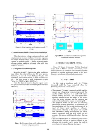
Figure 14. Matlab/ simulink model for PV–Grid integrated system.
[3] Khaligh A., " A Multiple-input dc-dc positive buck- [11] Matlab and Simulink, The Mathworks, Inc.,
boost converter topology", APEC2008, Twenty- version R2008a, http://www.mathworks.com
Third Annual IEEE, 24-28 Feb., 2008, pp.1522- [12] Hart D.W, " Power Electronics", Valparaiso
1526. University, 2010, McGraw Hill, pp.196-230.
[4] Ahmed N.A.," Modeling and simulation of ac-dc
buck-boost converter fed dc motor with uniform
PWM technique", Electric Power systems Research
73 (2005), pp363-372.
[5] Balkarishnan A.,Toliyat and Alexander W.C.," Soft
switched ac link buck-boost converter", APEC
2008, Twenty-Third Annual IEEE, 24-28 Feb.,
2008, pp.1334-1339.
[6] Santos J.L, Antunes F, Chehab A., and Cruz C.," A
maximum power point tracker for PV systems using
65](https://image.slidesharecdn.com/cmp0200-ieee-130115020213-phpapp02/85/Cmp0200-ieee-6-320.jpg)