Implementation Of A High-Efficiency, High-Lifetime, And Low-Cost Converter Using Photovoltaic System
•
0 likes•578 views

This paper proposes a new converter for photovoltaic water pumping and treatment systems without the use of storage elements. The converter is designed to drive a three-phase induction motor directly from PV solar energy. The use of this motor has the objective of presenting a better solution to the standard DC motor water pumping system. The development is oriented to achieve a commercially viable solution and a market friendly product. The converter topology is based on a Resonant Two Inductor Boost converter and a Threephase Voltage Source inverter achieving 90% efficiency at a rated power of 210W.

Recommended
Recommended
More Related Content
What's hot
What's hot (20)
Similar to Implementation Of A High-Efficiency, High-Lifetime, And Low-Cost Converter Using Photovoltaic System
Similar to Implementation Of A High-Efficiency, High-Lifetime, And Low-Cost Converter Using Photovoltaic System (20)
More from irjes
More from irjes (20)
Recently uploaded
Recently uploaded (20)
Implementation Of A High-Efficiency, High-Lifetime, And Low-Cost Converter Using Photovoltaic System
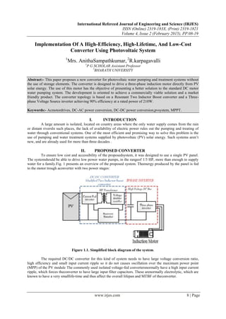
- 1. International Refereed Journal of Engineering and Science (IRJES) ISSN (Online) 2319-183X, (Print) 2319-1821 Volume 4, Issue 2 (February 2015), PP.08-19 www.irjes.com 8 | Page Implementation Of A High-Efficiency, High-Lifetime, And Low-Cost Converter Using Photovoltaic System 1 Mrs. AnithaSampathkumar, 2 R.karpagavalli 1 P G SCHOLAR Assistant Professor 2 BHARATH UNIVERSITY Abstract:- This paper proposes a new converter for photovoltaic water pumping and treatment systems without the use of storage elements. The converter is designed to drive a three-phase induction motor directly from PV solar energy. The use of this motor has the objective of presenting a better solution to the standard DC motor water pumping system. The development is oriented to achieve a commercially viable solution and a market friendly product. The converter topology is based on a Resonant Two Inductor Boost converter and a Three- phase Voltage Source inverter achieving 90% efficiency at a rated power of 210W. Keywords:- Acmotordrives, DC-AC power conversion, DC-DC power conversion,pvsystem, MPPT. I. INTRODUCTION A large amount is isolated, located on country areas where the only water supply comes from the rain or distant riversIn such places, the lack of availability of electric power rules out the pumping and treating of water through conventional systems. One of the most efficient and promising way to solve this problem is the use of pumping and water treatment systems supplied by photovoltaic (PV) solar energy. Such systems aren’t new, and are already used for more than three decades . II. PROPOSED CONVERTER To ensure low cost and accessibility of the proposedsystem, it was designed to use a single PV panel. The systemshould be able to drive low power water pumps, in the rangeof 1/3 HP, more than enough to supply water for a family.Fig. 1 presents an overview of the proposed system. Theenergy produced by the panel is fed to the motor trough aconverter with two power stages: Figure 1.1. Simplified block diagram of the system. The required DC/DC converter for this kind of system needs to have large voltage conversion ratio, high efficiency and small input current ripple so it do not causes oscillation over the maximum power point (MPP) of the PV module The commonly used isolated voltage-fed convertersnormally have a high input current ripple, which forces theconverter to have large input filter capacitors. These arenormally electrolytic, which are known to have a very smalllife-time and thus affect the overall lifepan and MTBF of theconverter.
- 2. Implementation Of A High-Efficiency, High-Lifetime, And Low-Cost Converter Using Photovoltaic System www.irjes.com 9 | Page Figure 1.2 Fig:1.3 Modified TIBC topology In this paper the previously mentioned resonant solutionwas implemented in the two inductor boost converter alongwith a voltage doubler rectifier Fig. 2(b), an innovativerecoverysnubber for this converter, Fig. 2(c), along with afixed duty cycle and a hysteresis controller. As a result the transformer is cheaper; theMOSFETs are cheaper, and the number of diodes in thesecondary side is halved. The regenerative snubber is formed of two diodes and acapacitor connecting the input side directly to the output sideof the converter, as showed in Fig. 2(c). This makes it a nonisolatedconverter, what have no undesirable effect in thephotovoltaic motor driver application. The voltage over theMOSFETs is applied to a capacitor connected to the circuitground and the voltage of this capacitor is coupled in series with the output of the rectifier..For the converter with the previously mentionedmodifications the static gain (k) can be calculated from (1),where D represents the duty cycle of each switch and must behigher than 50% to guarantee the necessary overlapping forthe correct operation ofthe TIBC converter= vout = output voltage vin = Input voltage k = Gain D = Duty cycle Ns/Np= Returns ratio
- 3. Implementation Of A High-Efficiency, High-Lifetime, And Low-Cost Converter Using Photovoltaic System www.irjes.com 10 | Page III. BLOCK DIAGRAM 3.2BLOCK DIAGRAM EXPLANATION PV A photovoltaic system (informally, PV system) is an arrangement of components designed to supply usable electric power for a variety of purposes, using the Sun (or, less commonly, other light sources) as the power source. PV systems may be built in various configurations: • Off-grid without battery (array-direct) • Off-grid with battery storage for DC-only appliances • Off-grid with battery storage for AC and DC appliances • Grid-tie without battery • Grid-tie with battery storage A photovoltaic array (also called a solar array) consists of multiple photovoltaic modules, casually referred to as solar panels, to convert solar radiation (sunlight) into usable direct current (DC) electricity. A photovoltaic system for residential, commercial, or industrial energy supply normally contains an array of photovoltaic (PV) modules, one or more DC to alternating current (AC) power converters (also known as inverters), a tracking system that supports the solar modules, electrical wiring and interconnections, and mounting for other components. Optionally, a photovoltaic system may include any or all of the following: renewable energy credit revenue-grade meter, maximum power point tracker(MPPT), battery system and charger, GPS solar tracker, energy management software, solar concentrators, solar irradiance sensors, anemometer, or task-specific accessories designed to meet specialized requirements for a system owner. The number of modules in the system determines the total DC watts capable of being generated by the solar array; however, the inverter ultimately governs the amount of AC watts that can be distributed for consumption. For example: A PV system comprising 11 kilowatts DC (kWDC) worth of PV modules, paired with one 10-kilowatt AC (kWAC) inverter, will be limited by the maximum output of the inverter: 10 kW AC. 3.2.1 Solar panel A solar panel is a set of solar photovoltaic modules electrically connected and mounted on a supporting structure. A photovoltaic module is a packaged, connected assembly of solar cells. The solar module can be used as a component of a larger photovoltaic system to generate and supply electricity in commercial and residential applications. Each module is rated by its DC output power under standard test conditions (STC), and typically ranges from 100 to 320 watts. The efficiency of a module determines the area of a module given the same rated output - an 8% efficient 230 watt module will have twice the area of a 16% efficient 230 watt module. Because a single solar module can produce only a limited amount of power, most installations contain multiple modules. A photovoltaic system typically includes a panel or an array of solar modules, an inverter, and sometimes a battery and or solar tracker and interconnection wiring.
- 4. Implementation Of A High-Efficiency, High-Lifetime, And Low-Cost Converter Using Photovoltaic System www.irjes.com 11 | Page 3.2.2 Theory and construction Solar modules use light energy (photons) from the sun to generate electricity through the photovoltaic effect. The majority of modules use wafer-based crystalline silicon cells or thin-film cells based on cadmium or silicon. The structural (load carrying) member of a module can either be the top layer or the back layer. 3.2.3 Efficiencies Depending on construction, photovoltaic modules can produce electricity from a range of frequencies of light, but usually cannot cover the entire solar range (specifically, ultraviolet, infrared and low or diffused light). Hence much of the incident sunlight energy is wasted by solar modules, and they can give far higher efficiencies if illuminated with monochromatic light. Therefore, another design concept is to split the light into different wavelength ranges and direct the beams onto different cells tuned to those ranges. This has been projected to be capable of raising efficiency by 50%. 3.3 THE ADVANTAGES OF SOLAR POWER • The fuel is free. • There are no moving parts to wear out, break down or replace. • Only minimal maintenance is required to keep the system running. • The systems are modular and can be quickly installed anywhere. • It produces no noise, harmful emissions or polluting gases 3.3.1 Maximum power point tracking (MPPT) Most energy production or storage devices have a complex relationship between the power they produce, the load placed on them, and the efficiency of the delivery. A conventional battery, for instance, stores energy in chemical reactions in its electrolytes and plates. These reactions take time to occur, which limits the rate at which the power can be efficiently drawn from the cell. For this reason, large batteries used for power storage generally list two or more capacities, 3.3.2 Isolating panels These problems have led to a number of different potential solutions that isolate panels individually or into much smaller groups (2 to 3 panels) in an effort to provide MPPT that avoids the problems of large strings. 3.3.3 Classification Controllers usually follow one of three types of strategies to optimize the power output of an array. Maximum power point trackers may implement different algorithms and switch between them based on the operating conditions of the array 3.3.4 Perturb and observe In one method, the controller adjusts the voltage by a small amount from the array and measures power; if the power increases, further adjustments in that direction are tried until power no longer increases. This is called the perturb and observe method and is most common, although this method can result in oscillations of power output.It is referred to as a hill climbing method, because it depends on the rise of the curve of power against voltage below the maximum power point, and the fall above that point. Perturb and observe is the most commonly used MPPT method due to its ease of implementation. Perturb and observe method may result in top-level efficiency, provided that a proper predictive and adaptive hill climbing strategy is adopted. 3.3.5 Current Sweep Method The current sweep method uses a sweep waveform for the PV array current such that the I-V characteristic of the PV array is obtained and updated at fixed time intervals. The maximum power point voltage can then be computed from the characteristic curve at the same intervals 3.3.6 Constant voltage The term "constant voltage" in MPP tracking is used to describe different techniques by different authors, one in which the output voltage is regulated to a constant value under all conditions and one in which the output voltage is regulated based on a constant ratio to the measured open circuit voltage (VOC). The latter technique is referred to in contrast as the "open voltage" method by some authors.If the output voltage is held constant, there is no attempt to track the maximum power point, so it is not a maximum power point tracking technique in a strict sense, though it does have some advantages in cases when the MPP tracking tends to fail,
- 5. Implementation Of A High-Efficiency, High-Lifetime, And Low-Cost Converter Using Photovoltaic System www.irjes.com 12 | Page and thus it is sometimes used to supplement an MPPT method in those cases.3.3.7 Comparison of methods.Both perturb and observe, and incremental conductance, are examples of "hill climbing" methods that can find the local maximum of the power curve for the operating condition of the array, and so provide a true maximum power point. 3.4 DC TO DC CONVERTERS A DC-to-DC converter is an electronic circuit which converts a source of direct current (DC) from one voltage level to another. It is a class of power converter.DC to DC converters are important in portable electronic devices such as cellular phones and laptop computers, which are supplied with power from batteries primarily. Such electronic devices often contain several sub-circuits, each with its own voltage level requirement different from that supplied by the battery or an external supply (sometimes higher or lower than the supply voltage). Additionally, the battery voltage declines as its stored power is drained. Switched DC to DC converters offer a method to increase voltage from a partially lowered battery voltage thereby saving space instead of using multiple batteries to accomplish the same thing.the excess power into a resistor, making them resistive dividers. Clearly, this is not quite ideal for the power conversion efficiency. 3.5 BOOST CONVERTER The boost converter is also known as step-up converter which produces an output voltage greater than the source. The ideal boost converter has the five basic components, namely a power semiconductor switch, a diode, an inductor, a capacitor and a PWM controller. The basic circuit which shows the placement of the inductor, the switch and the diode of the boost converter is shown in figure 3.4.2 Linear Voltage Converters The most elementary DC-DC converters are linear voltage converters. They achieve DC-DC voltage conversion by dissipating. Fig:3.1 When the switch S is ON, the current through the inductor increases and the energy stored in the inductor builds up. When the switch is off, current through the inductor continues toflow via the diode D, load and back to the source. The inductor is discharging its energy and the Polarity of inductor voltage is such that its terminal connected to the diode is positive with respect to its other terminal connected to the source. It can be seen then the capacitor voltage has to be higher than the source voltage and hence this converter is known as the boost converter. It can be seen that the inductor acts like a pump, receiving energy when the switch is closed and transferring it to the RC network when the switch is open. Fig 3.2 When the switch is closed the diode does not conduct and the capacitor sustains the output voltage. As long as the RC time constant is very much larger than the period of the switch , the output voltage would remain more or less constant. When the switch is open, there is a single connected circuit in this case.
- 6. Implementation Of A High-Efficiency, High-Lifetime, And Low-Cost Converter Using Photovoltaic System www.irjes.com 13 | Page 3.5.1 Inverters An inverter is a device that converts DC power from the battery bank to AC power for various loads. In larger systems that incorporate components that demand AC power, an inverter must be utilized. Also, if the instrument site is located some distance from the power production site, an inverter allows for an efficient means of getting electricity to the point of use. AC is easier to transport over long distances and has become the conventional modern electrical standard. 3.6 MOSFET Metal Oxide Semiconductor Field Effect Transistors (MOSFET) is a type of transistor. A MOSFET can be Created so that the power required to turn it on is considerably less than bi-polar junction transistors (BJT) Or Darlington transistors. MOSFETs can also be made to withstand more power and turn on faster than BJT or Darlington transistors. Most modern integrated circuits (IC) like micro-controllers are created using MOSFETS to increase their speed and lower power consumption. MOSFETS are transistors and can be used as switches. There are three pins on a MOSFET: gate, drain, and source. Gate voltage controls current flow though the transistor. There are four different types of MOSFETS. Fig.3.3Mosfet Symbols TABLE-I N-Channel Enhancement Mode N-Channel Depletion Mode P-Channel Enhancement Mode P-Channel Depletion Mode
- 7. Implementation Of A High-Efficiency, High-Lifetime, And Low-Cost Converter Using Photovoltaic System www.irjes.com 14 | Page 3.6.1 Depletion-mode MOSFET The Depletion-mode MOSFET, which is less common than the enhancement types is normally switched "ON" without the application of a gate bias voltage making it a "normally-closed" device. However, a gate to source voltage ( VGS ) will switch the device "OFF". Similar to the JFET types. For an N-channel MOSFET, a "positive" gate voltage widens the channel, increasing the flow of the drain current and decreasing the drain current as the gate voltage goes more negative. In other words, for an N-channel depletion mode MOSFET: +VGS means more electrons and more current. While -VGSmeans less electrons and less current. The opposite is also true for the P-channel types. Then the depletion mode MOSFET is equivalent to a "normally- closed" switch. 3.6.2 Enhancement-mode MOSFET The more common Enhancement-mode MOSFET is the reverse of the depletion-mode type. Here the conducting channel is lightly doped or even un doped making it non-conductive. This results in the device being normally "OFF" when the gate bias voltage is equal to zero. 3.7 PWM Pulse width modulation (PWM) is a powerful technique for controlling analog circuits with a microprocessor's digital outputs. PWM is employed in a wide variety of applications, ranging from measurement and communications to power control and conversion.Pulse-width modulation(PWM), or pulse- duration modulation (PDM), is a modulation technique that conforms the width of the pulse, formally the pulse duration, based on modulator signal information. Although this modulation technique can be used to encode information for transmission, its main use is to allow the control of the power supplied to electrical devices, especially to inertial loads such as motors. In addition, PWM is one of the two principal algorithms used in photovoltaicsolar battery chargers, the other being MPPT. Triangulation method (Natural sampling) Amplitudes of the triangular wave (carrier) and sine wave (modulating) are compared to obtain PWM waveform. Simple analogue comparatorcan be used. Basically an analogue method. Its digital version, known as REGULAR sampling is widely used in industry. 3.7.1 PWM types • Natural (sinusoidal) sampling (as shown on previous slide) – Problems with analogue circuitry, e.g. Drift, sensitivity etc. • Regular sampling – Simplified version of natural sampling that results in simple digital implementation • Optimized PWM PWM waveform is constructed based on certain performance criteria, e.g. THD. • Harmonic elimination/minimization PWM – PWM waveforms are constructed to eliminate some undesirable harmonics from the output waveform spectra. – Highly mathematical in nature • Space-vector modulation (SVM) – A simple technique based on volt-second that is normally used with three-phase inverter motor drive Modulation Index (Modulation Depth) M : 𝑀1= Amplitude of the carrier waveform Amplitude of the modulating waveform Modulation Ratio (Frequency Ratio) Mr:- 𝑀𝑟=𝜌= Frequency of the modulating waveform Frequency of the carrier waveform
- 8. Implementation Of A High-Efficiency, High-Lifetime, And Low-Cost Converter Using Photovoltaic System www.irjes.com 15 | Page 7.2 Sine wave Alternating current has continuously varying voltage, which swings from positive to negative. This has an advantage in power transmission over long distance. Power from the Grid is carefully regulated to get a pure sine wave and also the sine wave radiate the least amount of radio power during long distance transmission. But it is expensive to generate sine wave in an inverter. Its quality is excellent and almost all electrical and electronic appliances work well in sine wave inverter. The sine wave is the AC waveform we get from the domestic lines and from the generator. The major advantage of sine wave inverter is that all of the house hold appliances are designed to operate in sine wave AC. Another advantage is that the sine wave is a form of soft temporal rise voltage and it lacks harmonic oscillations which can cause unwanted counter forces on engines, interference on radio equipments and surge current on condensers. 3.7.2 Modified Sine wave or Quasi Sine wave Modified sine wave is designed to simulate a sine wave since the generation of sine wave is expensive. This waveform consists of a Flat Plateau of positive voltage, dropping abruptly to zero for a short period, then dropping again to a flat plateau of negative voltage. It then go back to zero again and returning to positive. This short pause at zero volts gives more power to 50 Hz fundamental frequency of AC than the simple square wave. 3.8 VOLTAGE DOUBLER A voltage doubler is an electronic circuit which charges capacitors from the input voltage and switches these charges in such a way that, in the ideal case, exactly twice the voltage is produced at the output as at its input. Voltage doublers are a variety of voltage multiplier circuit. Many (but not all) voltage doubler circuits can be viewed as a single stage of a higher order multiplier: cascading identical stages together achieves a greater voltage multiplication. 3.9 SNUBBER CIRCUIT A snubber is a device used to suppress some phenomenon. Protection of switching devices and circuits: Switching devices and circuit components may fail due to the following reasons. 1. Overheating – thermal failure 2. Overcurrent 3. Overvoltage – usually happens during turn-off 4. Excessive di/dt 5. Excessive dv/dt 6. Switching loss –excessive switching loss is a major contributing factor of overheating. Power electronic circuits and their switching devices and components can beprotected from overcurrent by placing fuses at suitable locations. Heat sinks, fins andfans are used to take the excess heat away from switching devices and other components. Snubber circuits are required to limit di/dt , dv/dt and overvoltage during turn-on and turnoff.Some typical snubber circuits are
- 9. Implementation Of A High-Efficiency, High-Lifetime, And Low-Cost Converter Using Photovoltaic System www.irjes.com 16 | Page RC snubber circuit Diode snubber circuit BJT Snubbers Overvoltage snubber 3.9.1 RC Snubber Circuits RC snubber circuits are normally connected across a switching device to limit thedv/dt.. An RC snubber circuit can be polarized or unpolarized. A forward-polarized RCsnubber circuit shown in Figure 1 is appropriate when a thyristor or a transistor isconnected with an anti-parallel diode. R limits the forward dv/dtand R1 limits the discharge current of the capacitor when Q1 is turned on. Figure 3.7 A forward polarized snubber circuit A reverse polarized snubber circuit as shown in Figure 2 is used to limit theReverse dv/dt.. R1 limits the discharge current of the capacitor. Figure 3.8A reverse polarized snubber circuit. An unpolarizedsnubber circuit as shown in Figure 3 should be used when a pairof switching devices is connectedinanti-parallel. Figure 3.9 Anunpolarizedsnubber circuit 3.10 RESONANT TANK An LC circuit, also called a resonantcircuit, tankcircuit, or tunedcircuit, consists of an inductor, represented by the letter L, and a capacitor, represented by the letter C. When connected together, they can act as an electrical resonator, an electrical analogue of a tuning fork, storing energy oscillating at the circuit's resonant frequency. Fig:3.10LC circuit diagram
- 10. Implementation Of A High-Efficiency, High-Lifetime, And Low-Cost Converter Using Photovoltaic System www.irjes.com 17 | Page 3.10.1 Applications The resonance effect of the LC circuit has many important applications in signal processing and communications systems.The most common application of tank circuits is tuning radio transmitters and receivers. For example, when we tune a radio to a particular station, the LC circuits are set at resonance for that particular carrier frequency.A series resonant circuit provides voltage magnification. 1. A parallel resonant circuit provides current magnification. 2. Aparallel resonant circuit can be used as load impedance in output circuits of RF amplifiers. Due to high impedance, the gain of amplifier is maximum at resonant frequency. 3. Both parallel and series resonant circuits are used in induction heating. LC circuits behave as electronic resonators, which are a key component in many applications: Amplifiers Oscillators Filters Tuners Mixers Foster-Seeley discriminator Contactless cards 3.11INDUCTION MOTOR One of the most common electrical motorused in most applications which is known as induction motor. This motor is also called as asynchronous motor because it runs at a speed less than synchronous speed. In this, we need to define what is synchronousspeed. Synchronous speed is the speed of rotation of the magnetic field in a rotary machine and it depends upon the frequency and number poles of the machine. An induction motor always runs at a speed less than synchronous speed because the rotating magnetic field which is produced in the stator will generate flux in the rotor which will make the rotor to rotate, but due to the lagging of flux current in the rotor with flux current in the stator, the rotor will never reach to its rotating magnetic field speed i.e. the synchronous speed. Working Principle of Induction Motor.But in induction motor we give only one supply, so it is really interesting to know that how it works. It is very simple, from the name itself we can understand that there is induction process occurred. Actually when we are giving the supply to the stator winding, flux will generate in the coil due to flow of current in the coil. Now the rotor winding is arranged in such a way that it becomes short circuited in the rotor itself. The flux from the stator will cut the coil in the rotor and since the rotor coils are short circuited, according to Faraday's law of electromagnetic induction, current will start flowing in the coil of the rotor. When the current will flow, another flux will geteneratedin the rotor. 3.12 TYPES INDUCTION MOTORSINGLE PHASE INDUCTION MOTOR 1. Capacitor start induction motor 2. Capacitor start capacitor run induction motor 3. Shaded pole induction motor automatically without any external force to the machine, then it is called as self starting. For example we see that when we press the key the fan starts to rotate automatically, so it is self starting. Point to be note that fan used in home appliances is single phase induction motor but it is self starting. How? We will discuical power systems are combinations of electrical circuits. IV. MATLABSIMULATIONRESULT INPUT VOLTAGE Fig:4.1
- 11. Implementation Of A High-Efficiency, High-Lifetime, And Low-Cost Converter Using Photovoltaic System www.irjes.com 18 | Page DOUBLER VOLTAGE Fig4.3 Switching pulse for M2 Fig 4.4 rotor speed,torque,stator current Fig:4.5
- 12. Implementation Of A High-Efficiency, High-Lifetime, And Low-Cost Converter Using Photovoltaic System www.irjes.com 19 | Page V. CONCLUSION In this paper, a converter for photovoltaic water pumping and treatment systems without the use of storage elements waspresented. The converter was design to drive a three phaseinduction motor directly from PV solar energzand wasconceived to be a commercially viable solution having lowcost, high efficiency, and highrobustness.Thepaper presented the system block diagram,control algorithm and desing. The experimental results suggest that the proposed solution could be a viable solution to this problem after morereliability tests are performed to guarantee its robustness. REFERENCE [1]. IEEE, PELS, “The IEEE 2011 Internaci Future Energy Challenge Request for Proposals”, Out 2010. [2]. E.H.P. Andrade, L.D.S. Bezerra, F. L.M. Antunes, M.R.B. Neto“Sistema de Bombeamento de Água com Energia Solar FotovoltaicaUtilizando Motor de InduçãoTrifásico” Sept 2008 (in português). [3]. Hahn, A. Technical maturity and relia ability of photovoltaic pumping systems. In: 13th European Photovoltaic Solar Energy Conference, NiceFrance, pp. 1783-1786. 1995. [4]. Vitorino, M.A.; Correa, M.B.R., " High performance photovoltaicpumping system using induction motor," Power ElectronicsConference, 2009. COBEP '09.Braziliavol., no., pp.797-804, Sept27 2009- Oct. 1 2009. [5]. Harsono, H., “Photovoltaic Water Pump System”, Kochi University ofTechnology, dissertation, august 2003. [6]. Linden, “Handbook of Batteries and Fuel Cells”, McGraw Hill, Inc.,1984. [7]. Tschanz, D.; Lovatt, H.; Vezzini, A; Perrenoud, V; "A multitfunctional converter for a reduced cost ,solar powered,water pump,” International Symposium onIndustrial Electronics (ISIE), 2010 IEEvol., no., pp.568-572, 4-7 July 2010. [8]. S. R. Bowes and A. Midoun, "Sub optimal swiching strategies formicroprocessor controlled PWM inverter drives," IEE Proceedings,vol. 132, Pt. B, no. 3, p. 133-148, May 1 1985 [9]. Cacciato, M.; Consoli, A.; Crisafulli, V.; , "A high voltage gain DC/DC converter for energy harvesting in single module photovoltaic applications," Industrial Electronics (ISIE), 2010 IEEE InternationalSymposium on , vol., no., pp.550-555, 4-7 July 2010. [10]. P. J. Wolfs, “A Current-Sourced Dc-Dc Converter Derived via the Duality Principle from the Half- Bridge Converter,” IEEE Trans. Industrial Electronics, Vol. 40, No. 1, pp. 139-144, Feb. 1993.