1) Alameda Applied Sciences Corp. is a small R&D firm focused on pulsed plasma coating technologies, funded by various government contracts.
2) They have developed a cathodic arc coating process called Coaxial Energetic Deposition that uses high voltage pulses to produce uniform, high quality coatings.
3) They have tested coatings for SRF applications and demonstrated good adhesion, high crystalline quality, and compatibility with complex geometries after tests like thermal cycling, pressure washing, and mechanical flexing. Tests were done in partnership with several national laboratories.
Krishnan - Energetic Condensation Growth of Nb films for SRF Acceleratorsthinfilmsworkshop
http://www.surfacetreatments.it/thinfilms
Energetic Condensation Growth of Nb films for SRF accelerators (Mahadevan Krishnan - 30')
Speaker: Mahadevan Krishnan - Alameda Applied Sciences Corporation | Duration: 30 min.
Abstract
AASC, Jefferson Lab and NSU conduct research into new SRF thin-film coatings by first characterizing the materials properties such as morphology, grain size, crystalline structure, defects, and impurities, then measuring properties such as Tc and RRR and following this with ‘in-cavity’ RF measurements of the Surface Impedance of the films at cryogenic temperatures. These progressive steps are essential to the eventual design of SRF accelerator structures and to measure Q-slope and other performance parameters at high fields.
This paper describes recent results from pure Nb thin-films grown on a-plane and c-plane sapphire, MgO as well as on amorphous substrates. Substrate preparation is shown to be critical to good electrical properties of the film. The sapphire and MgO substrates were heated up to 700 deg C and subsequently coated at 300, 500 and 700 deg C. Film thickness was varied from ~0.25µm up to >3µm. RRR and Tc were measured. The XRD data yielded pole figures, intensity vs. 2-θ and intensity vs. φ plots. These data were complemented by EBSD and SEM images. RRR values ranging from ~10 up to ~333 have been measured and correlated with the XRD data. Good crystallinity is associated with high RRR. Single crystalline (110) epitaxial layers of Nb films are grown well on a-plane sapphire substrates at different temperatures. Nb films have also been grown on Cu substrates, as well as on MgO and borosilicate substrates. The significance of crystalline structure observed on amorphous substrates is discussed in light of its implications for future, lower-cost SRF cavities.
Phillips - Atomic Layer Deposition of NbN Thin Films for Superconducting Radi...thinfilmsworkshop
http://www.surfacetreatments.it/thinfilms
Atomic Layer Deposition of NbN thin films for SRF applications (Larry Phillips - 15')
Speaker: Larry Phillips - Jefferson Lab - Newport News - Virginia | Duration: 15 min.
Abstract
Niobium Nitride is a 17K superconductor investigated since early eighthies for Superconducting Radiofrequency applications.
Atomic Layer deposition is instead a technique that only recently starts to be considered for industrial applications.
Mahadevan krishnan coaxial energetic deposition of thin filmsthinfilmsworkshop
AASC has been studying thin film coating of Nb on coupon substrates as well as on1300MHz RF cells. At the last Thinfilm workshop in Padua, we reported on high RRR measurements and good crystallinity in Nb films coated onto crystal substrates such as a-sapphire, MgO and also on polished Copper coupons. Since then, we have coated several 1300MHz RF cells provided to us and tested by LANL, ANL and JLab. The Qo vs. E measurements suggest that better surface preparation is a must for high quality RF performance. Future work will coat Copper cells with different surface preparation (centrifugal barrel polishing and EP) and try to improve upon our preliminary results. Results from Nb films coated on to Al6061 coupons are encouraging and motivate coating of a barrel polished Aluminum RF cell. Recently AASC has embarked upon two new thinfilm coating projects: Nb on stainless steel bellows for SRF accelerators and Cu films on stainless steel tubes for high power RF Couplers. We are also collaborating with CERN to coat a Cu disk of a quadrupole resonator with Nb, for RF tests at high fields. This talk will provide details of all of these ongoing activities, all of which are supported by the US Department of Energy via SBIR contracts.
It's What's Inside That Counts - Nanosilica Filled AdhesivesMaster Bond
Learn about Master Bond’s nanosilica filled systems offering enhanced abrasion resistance and dimensional stability.
These specialty formulations feature superior physical properties as well as low shrinkage upon curing. View to learn more!
Anne marie valente feliciano - nucleation of nb films on cu substratesthinfilmsworkshop
In the pursuit of niobium (Nb) films with similar performance with the commonly used bulk Nb surfaces for Superconducting RF (SRF) applications, significant progress has been made with the development of energetic condensation deposition techniques. The controlled incoming ion energy enables a number of processes such as desorption of adsorbed species, enhanced mobility of surface atoms and sub-implantation of impinging ions, thus producing improved film structures at lower process temperatures. All these along with the quality of the Cu substrate have an important influence on the nucleation and subsequent growth of the Nb film, creating a favorable template for growing the final surface exposed to SRF fields. This contribution shows how the structure and defect density thus electron mean free path (represented by residual resistance ratio values) of Nb films can be tailored on Cu substrates, by varying the ion energy and thermal energy provided to the substrate, favoring the hetero-epitaxial or the fiber growth mode.
Journal of Thin Films, Coating Science Technology and Application vol 3 issue 3STM Journals
Journal of Thin Films, Coating Science Technology and Application (JoTCSTA) Publishes Review /Research articles and attempts to bring out latest cutting –edge technologies in the field of coating technology, Subject areas suitable for publication include ,but are not limited to the following fields
Focus and Scope Covers
Biomaterials, colloid and surface chemistry
Adhesion, contact mechanics and Coatings Technology
Friction and wear, including mechanisms, modeling, characterization, measurement and testing
lubricants and Lubrication technology and applicarion
Coatings and surface treatments and Surface integrity
Tribology of composite materials: metallic, polymeric and ceramic and Tribological applications
Surface modifications, including surface cladding, cutting, polishing and grinding
material science, manufacturing , foundry, welding, joining, composites manufacturing
thermal and plasma spraying, thermo-chemical treatment,
Plating, sol-gel coating, anodization, plasma electrolytic oxidation, etc., but excluding painting.
Corrosion, friction performance and wear resistance
Surfaces, Interfaces, Thin Films, Corrosion and Coatings
Electroless and Friction based coating, Coatings for biological applications and High temperature applications
Correlation between the Interface Width and the Adhesion Strength of Copper F...IOSRJAP
The present study has been conducted in order to determine the influence of negative bias voltage applied to substrate on adhesion of copper films deposited on carbon steel substrates. The adhesion strength has been evaluated by the scratch test. Coatings were deposited by a DC magnetron sputtering system. The substrates were firstly mechanically polished and then ion-etched by argon ions prior to deposition. Adhesion was found to increase with the bias voltage. The critical load had a value of 9.5 g for an unbiased substrate and reached 18.5 g for a bias voltage of 600 V. Equally important, the interface width, measured using Auger electron spectroscopy, increased as a function of the bias voltage. The width of the interface is related to the time of ion milling in the Auger spectrometer. The size of this width is obtained from the Auger elemental depth profiles through measuring the depth of the interface coating/substrate. The width had a value of 335 min with a bias of 600 V whereas it didn't exceed 180 min when the substrate was unbiased. Therefore, the effect of the bias voltage was to expand the interface because of the diffusion phenomenon and physical mixing of materials at the interface. Moreover, the critical load increased with the increase of the interface width.
Influence of Thickness on Electrical and Structural Properties of Zinc Oxide ...paperpublications3
Abstract: Zinc Oxide (ZnO) thin films were prepared on corning (7059) glass substrates at a thickness of 75.5 and 130.5nm by RF sputtering technique. The deposition was carried out at room temperature after which the samples were annealed in open air at 1500C. The electrical and structural properties of these films were studied. The electrical properties of the films were monitored by four-point probe method while the structural properties were studied by X-ray diffraction (XRD). It was found that the electrical resistance of the films decreases with increase in the thickness of the films. The XRD analysis of the films showed that the films have a peak located at 〖34.31^0-34.35〗^0with hkl (002). Other parameters calculated include the stress ( ) and the grain size (D).
Rosa alejandra lukaszew a review of the thin film techniques potentially ap...thinfilmsworkshop
SRF is a surface phenomenon where only ~10 penetration depths are needed (l=40 nm for niobium), thus it has been recognized for some time now that it would be economically convenient to use thin film coated cavities. But problems arise with defects within 1 or 2 l of the surface or on the surface, and insufficient attention has been paid to this topic, including trapping of impurities like oxygen in defects as well as surface roughness enabling magnetic field pinning sites. Earlier attempts at CERN applied standard sputter PVD methods, but the grain size for the CERN Nb/Cu films was 100 nm, which is 10,000 times smaller than for conventional SRF cavities with the ensuing problems that appear at grain boundaries. Thus, these prior attempts showed higher surface resistance and worst Q-slope than bulk. I will review more modern approaches using higher energetic PVD methods for thin film deposition which offer promise to achieve thin films with improved superconducting performance.
IJERA (International journal of Engineering Research and Applications) is International online, ... peer reviewed journal. For more detail or submit your article, please visit www.ijera.com
IJERA (International journal of Engineering Research and Applications) is International online, ... peer reviewed journal. For more detail or submit your article, please visit www.ijera.com
Studies on in-Doped Zno Transparent Conducting thin FilmsIJRESJOURNAL
ABSTRACT: In this manuscript we have investigated the influences of indium dopants on zinc oxide (ZnO) thin films regarding physico-chemical properties for application in modern conducting devices. As a starting material, Indium (III) chloride, and Zn(CH3COO)2⋅2H2O were used. The complex TSDC spectrum was obtained by submitting the sample to a constant electrical field Ep = 10M V/m during 2 min at a varing polarization temperature of Tmax = 1500C. A minimal sheet resistance with electrical resistivity as low in the range of 10-3 Ω·cm was found for this thin film.
Surface Morphological and Electrical Properties of Sputtered Tio2 Thin FilmsIOSR Journals
Titanium dioxide films were formed on quartz and crystalline p-Si (100) substrates by DC reactive magnetron sputtering method. Pure titanium target was sputtered at a constant oxygen partial pressure of 5x10⁻² Pa, and at different sputtering powers in the range 80 – 200 W. The as-deposited films were annealed in air for 1 hour at 1023 K. The deposited films were characterized by studying the surface morphology by atomic force microscopy (AFM), electrical and dielectric properties from current-voltage and capacitance-voltage measurements. Atomic force micrographs of the films showed that the Rrms and Ra increased with the increase of sputter power from 80 to 200 W. The leakage current density was increased by increasing the sputtering power.
Research Inventy : International Journal of Engineering and Science is published by the group of young academic and industrial researchers with 12 Issues per year. It is an online as well as print version open access journal that provides rapid publication (monthly) of articles in all areas of the subject such as: civil, mechanical, chemical, electronic and computer engineering as well as production and information technology. The Journal welcomes the submission of manuscripts that meet the general criteria of significance and scientific excellence. Papers will be published by rapid process within 20 days after acceptance and peer review process takes only 7 days. All articles published in Research Inventy will be peer-reviewed.
This to demonstrate the laser ablation of hard materials to form a thin film for optical sensors. The work was done at DIllard University , New Orleans LA by Professor Abdalla Darwish. any comment e-mail adarwish@bellsouth.net.
Different types of Nanolithography technique.
Types: Electron beam lithography, Photolithography, electron-beam writing, ion- lithography, X-ray lithography, and related images, concepts and graphical views.
I hope this presentation helpful for you.
https://www.linkedin.com/in/preeti-choudhary-266414182/
https://www.instagram.com/chaudharypreeti1997/
https://www.facebook.com/profile.php?id=100013419194533
https://twitter.com/preetic27018281
Please like, share, comment and follow.
stay connected
If any query then contact:
chaudharypreeti1997@gmail.com
Thanking-You
Preeti Choudhary
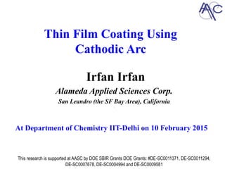
1. Thin Film Coating Using
Cathodic Arc
Irfan Irfan
Alameda Applied Sciences Corp.
San Leandro (the SF Bay Area), California
`
This research is supported at AASC by DOE SBIR Grants DOE Grants: #DE-SC0011371, DE-SC0011294,
DE-SC0007678, DE-SC0004994 and DE-SC0009581
At Department of Chemistry IIT-Delhi on 10 February 2015
2. Small R&D firm, started in
1994 by Dr. Mahadevan
Krishnan.
Since inception main focus
has been the application of
Pulsed Plasma Technology.
Funded substantially by
different government
contracts.
Alameda Applied Sciences Corporation:
3. Limited success in past
commercialization
attempts.
Currently more focused on
SRF coatings and fast gas
valves for LPA.
Alameda Applied Sciences Corp. Contd.:
4. Cathodic Arc Coating (Ion Energy):
Comparison of Stress build-up in low energy
deposition, energetic condensation, and energetic
condensation plus high voltage bias
[*] M. M. Bilek, R N. Tarrant, D. R. McKenzie, S H. N. Lim, and D G. McCulloch “Control of Stress and Microstructure in Cathodic Arc Deposited
Films” IEEE TRANSACTIONS ON PLASMA SCIENCE, VOL. 31, NO. 5, OCTOBER 2003
(A. Bendavid, CSIRO)
(M.M. Bilek)
* A. BENDAVID, P. J. MARTIN, R. P. NETTERFIELD, G. J.
SLOGGETT, T. J. KINDER, C., ANDRIKIDIS, JOURNAL OF
MATERIALS SCIENCE LETTERS 12 (1993) 322-323
Ion energy, eV
f(e)
Nb
5. Energetic Condensation (Crystal Growth):
In Energetic Condensation, the ions deposit energy in a sub-surface layer (≈3-5 atomic
layers deep for ~100eV Nb ions), shaking up the lattice, causing adatom mobility and
promoting epitaxial crystal growth
Energetic Condensation, when combined with substrate heating, promotes lower-defect
crystal growth
J.A. Thornton, "Influence of substrate temperature and deposition rate on the structure of thick sputtered Cu coatings”, J. Vac. Sci.
Technol. Vol. 12, 4 Jul/Aug 1975
Andre Anders, A structure zone diagram including plasma-based deposition and ion etching, Thin Solid Films 518 (2010) 4087–4090
6. ~30-100 V applied between a desired cathode and an anode mesh.
A triggering event at one side initiates one pulse of coating.
Averaged over many pulses it creates a uniform ~1 monolayer/pulse coating.
Coaxial Energetic Deposition:
Coaxial Energetic Deposition (CEDTM)
7. SRF Coating Requirements:
Test Why
Film ADHESION with frequent cooling
and heating: Thermal Shocks
For operation at 2-4 oK
Film ADHESION with >500 psi water
rinse: Mechanical Shocks
To remove particulates and secondary
ion emission sites
Film ADHESION with: Mechanical
Flex
For connecting RF cavities/cells
(stainless steel bellows)
High Crystalline growth: High RRR For acceleration gradient in >1010
eV/m (no quenching) => Low
resistance (BCS limit and low defects)
Compatibility with Complex
Geometries
For coating real accelerator hardware,
RF cells, Power Couplers
11. High pressure water rinse (HPWR) on ~3 mm thick12 mm x 50 mm bars.
All survived well beyond 500 psi.
Tested at Fermi Lab by Curtis Crawford
Mechanical Shock:
12. CERN Resonator Plate-II:
5 min. in a 20g/l sulfamic acid -> 20 min. rinse in distilled water -> in IPA bath till mounting.
3.4 micron film at center and ~2 around edges.
Survived ~80 psi at CERN, tested by Sarah Aull.
13. The Nb film survived repeated cycles of HPWR at up to (80Bar) 500psi.
Tested at Los Alamos N Lab by T. Tajima
Nb Coated Cu 1.3 GHz Cell:
KEK-06 Cu cavity before Nb coating KEK-06 Cu cavity after Nb coating
14. Mechanical Flex on Bellows:
Starts in Expanded position 3.5”
Compressed to 2.6” in 1 sec,
stays 0.5 sec
Back to expanded position in 1
sec, stays 0.5 sec
24,000 times (~20 Hrs)
Rinsed, filtered and analyzed for
particles that may come off
during the mechanical flex test
Tested at BNL by Bin Ping et al
15. High RRR films:
HPWR 500 psi at FNAL, RRR≈52 in our Cu films
Temple Univ. measured AASC Cu on SS strips RRR~42 – 64
XFEL Germany requirements >30
Stainless steel tube coated with a ~28µm
Cu film using the AASC CED process
Copper surface after 86Bar HPWR test
(courtesy of Curtis Crawford/FNAL)
16. High RRR on coupons motivates coating accelerator structures
RRR-585 measured on 5µm
film on MgO
RRR-330 measured on a-
sapphire
M Krishnan, E Valderrama, B Bures, K Wilson-Elliott, X Zhao, L Phillips, A-M Valente-Feliciano, J Spradlin, C
Reece and K Seo, “Very high residual-resistivity ratios of heteroepitaxial superconducting niobium films on MgO
substrates,” Superconductor Science and Technology , vol. 24, p. 115002, November 2011
M. Krishnan, E. Valderrama, C. James, X. Zhao, J. Spradlin, A-M Valente Feliciano, L. Phillips, and C. E. Reece,
K. Seo, Z. H. Sung, “Energetic condensation growth of Nb thin films”, PHYSICAL REVIEW SPECIAL TOPICS -
ACCELERATORS AND BEAMS 15, 032001 (2012).
110 & 200 200110
Polycrystalline
Monocrystal
with two
orientations
Monocrystal
with 100
orientation
RRR=7, 150/150 RRR=181, 500/500 RRR=316, 700/700
Change in crystal
orientation from 110 to 200
at higher temperature
RRR
RRR
17. Compatibility with Complex Geometries:
Coating inner surface of bellows.
Coating outer surface of tubes.
Coating inner surface of long tubes.
HPWR 500 psi at FNAL all survived except the
tube coated outside.
18. RF test of Nb Film:
Nb coating on 2” Cu single crystal.
RF measurement by Paul Welander at SLAC-Stanford.
19. Current State of the Art Bulk Nb:
N doped bulk Nb cavities from FNAL.
AASC Nb coating on KEK06, RF measurements by T. Tajima at LANL.
1.E+05
1.E+06
1.E+07
1.E+08
1.E+09
0 2 4 6 8 10
Q0
Eacc (MV/m)
4 K
<2 K
20. Thank You
AASC
Mahadevan Krishnan,
Steven Chapman,
Katherine Velas
Los Alamos N. Lab
Tsuyoshi Tajima..
CERN
Sarah Aull..
Fermi Lab
Curtis Crawford,
Lance Cooley..
Brookhaven N. Lab
Sergey, Bin Ping..
Jefferson Lab
Rong Li, C. Reece…
Argonne N. Lab
Thomas Prolier..
SLAC (Stanford)
Paul Welander..
SLAC (Stanford)
Xiaoxing Xi..