SlideShare a Scribd company logo
Prof. Yonhua Tzeng
Diamond and Devices Lab
Department of Electrical Engineering
National Cheng Kung University
Diamond & Devices Lab
成功大學與德國烏爾姆大學合作
Collaboration between NCKU (Taiwan) and Ulm University (Germany)
(1.) Hydrogen generation with transparent boron doped diamond (BDD) electrodes
(a.) Diamond electrodes on sapphire
(b.) Diamond electrodes on silicon membrane
Nanodiamond for electrochemical and high power electronic applications
Fabrication of electrodes on silicon
 bias-enhanced nucleation (BEN)
 growth of diamond films in HFCVD
 E-beam lithography and thermal
evaporator to form metallic clusters
 etching of silicon to form diamond membrane
Motivation
Diamond is an electrochemically stable
electrode material and is an transparent
layer on a semiconductor solar cell
 immerse a solar cell panel in water
with gas bubbles floating off from the
surface.
 it does not corrode in the cathodic
regime and does not form an oxide
layer under anodic polarization.
 neither cathodic nor anodic
polarization leads to etching of
diamond
Modifying diamond electrodes by metallic
micro dots to reduce the water splitting
redox potential window (3V)
 metallic clusters on diamond surface
need to be stable in expected
operating environments
 the metallic clusters can narrow the
potential window with remaining
diamond electrode staying transparent
Transparent diamond film
 inductively coupled plasma etching
 sulfur hexafluoride gas
Publications
Cyclic voltammetry of boron doped
diamond electrode and boron doped
diamond modified by titanium and
platinum micro dots 0.25 % and 11%
surface coverage.
Narrow the potential window
Enhance the current density
Electrochemical measurement
cluster diameter: 2 µm
distance: 6 µm
surface coverage: 11%
Optical microscope photo
Poster# P130
C. Li, Y. Tzeng, E. Kohn, M. Dipalo C.Liu,
“Electrochemical and Optical Properties
of Electrode with A Metallic Microdot
Array on Boron Doped Diamond.”
Poster# P176
 Z. Gao, Y. Xu, C. Pietzka, E. Kohn,
“Water Splitting with Transparent
Diamond Electrodes.”
(2.) Investigation of diamond nucleation
-- Comparison of electrochemical activities of nanodiamond deposited on silicon with diamond seeding and bias enhanced nucleation
(3.) (a) lnAIN growth on GaN at NCKU (b) Diamond seeding and growth at NCKU (c) Patterning and fabrication of HEMT at Ulm
Growth temp. 750 °C
Gas conc. 0.3 % CH4 in H2
Growth rate 0.12 µm/hr
InAlN/GaN HEMT on sapphire
- 200 nm Si3N4 passivation
- standard metallization
Processed in Ulm
Motivation
Publications
Motivation
BDD
Intrinsic Diamond
Sapphire Substrate
Diamond Seeding
After 500 nm growth
Results
Seeding with nano particles(NCKU)
Fabrication of HEMT (Ulm)
MOCVD growth of lnAIN/GaN on
sapphire (NCKU)
Device and materials analysis
(Ulm and NCKU)
Heat sink
-4 -3 -2 -1 0 1 2 3
-20
-15
-10
-5
0
5
10
15
20
Currentdensity(mA/cm2
)
Potential vs Ag/AgCl (voltage)
BDD/Ti/Pt (0.25% coverage)
BDD/Ti/Pt (11% coverage)
BDD
No microdots
11% coverage by microdots
0.25% coverage by microdots
Transmittance spectrum
Diamond for heat extraction
Poster# P147
 Z. Gao, Y. Lin, E. Colombo, Y. Liu, Y. Tzeng, E. Kohn,“Effects of
Seeding, BEN and CVD Processes on Optical Transparency of
Quasi-metallically Doped NCD Electrodes Grown on Insulating
Substrates.”
 joint posters at 4th NDNC (New Diamond
and Nano Carbons) conference in China,
May 16-20, 2010
Si
NCD
BDD 1 μm
1 μm
500μm
Si
Ti
Pt
 Diamond films on transparent substrate
are important for bio-MEMs
 Deposition of Diamond films on non-
diamond substrates needs seeding by
nanodiamond particles or nucleation from
carbide clusters (metal carbides or SiC)
 Carbide clusters are not transparent but
form a stable interface
 Seeding by nanodiamond particles does
not hinder transparency but is
challenging to form a stable interface with
the substrate, compromising adhesion.
Contribution to existing EU-FP7
project MORGAN.
Improve the cooling capability of a
GaN power FET.
 Thermal management of GaN power
FETs by a top diamond heat spreader
using NCKU seeding method for
diamond layer growth.
0 2 4 6 8 10 12
0.0
0.1
0.2
0.3
0.4
0.5
0.6
-7 V
LG
= 0.5 痠
-6 V
-5 V
-2 V
VDS
(V)
IDS
(A/mm)
-4 V
-3 V
-1 V
0 V
1 V
2 V
3 Vμm
 Participation in MORGAN follow-up project proposed
Prof. Erhard Kohn
Materials and Devices Group
Inst. of Electron Devices and Circuits
Ulm University
joint poster at 4th NDNC (New Diamond and Nano Carbons)
conference in China, May 16-20, 2010
Acknowledgement
Financial support by NSC Taiwan under the grants (NSC-98-3114-M-
006-001, NSC-96-2221-E-006-286-MY3, NSC-98-2911-I-006-031,
NSC-99-2915-I-006-015) is highly appreciated.
• Only Seeding (NCKU)
• Seeding (NCKU) + MPCVD (NCKU)
• BEN(Ulm) + MPCVD (Ulm)
1 μm nano-crystal diamond (NCD)
1 μm boron doped diamond
Sapphire Substrate
Diamond Seeding

More Related Content

What's hot

ECS 2008 Presentaion
ECS 2008 PresentaionECS 2008 Presentaion
ECS 2008 Presentaionpinkfans5
 
Energia r.p.h.chang
Energia r.p.h.changEnergia r.p.h.chang
Energia r.p.h.chang
Cesar Diaz
 
Daytona Beach Conference Aluminum Oxide And Silicon Nitride Thin Films As (2)
Daytona Beach Conference  Aluminum Oxide And Silicon Nitride Thin Films As (2)Daytona Beach Conference  Aluminum Oxide And Silicon Nitride Thin Films As (2)
Daytona Beach Conference Aluminum Oxide And Silicon Nitride Thin Films As (2)
Lin Lin
 
Effects of ionizing radiation on the layered semiconductor tungsten diselenide
Effects of ionizing radiation on the layered semiconductor tungsten diselenideEffects of ionizing radiation on the layered semiconductor tungsten diselenide
Effects of ionizing radiation on the layered semiconductor tungsten diselenide
Roger Walker
 
UMKC - Perovskite Solar Cells
UMKC - Perovskite Solar CellsUMKC - Perovskite Solar Cells
UMKC - Perovskite Solar Cells
kphodel
 
vlsi fabrication
vlsi fabricationvlsi fabrication
vlsi fabrication
Srikanth Vas
 
Synthetic Diamond for Aerospace Applications
Synthetic Diamond for Aerospace ApplicationsSynthetic Diamond for Aerospace Applications
Synthetic Diamond for Aerospace Applications
mikegem
 
Crystal microphone
Crystal microphoneCrystal microphone
Crystal microphone
Gyan Jyoti Gogoi
 
KCG+GFC Introduction PPT_Final_EN_v1
KCG+GFC Introduction PPT_Final_EN_v1KCG+GFC Introduction PPT_Final_EN_v1
KCG+GFC Introduction PPT_Final_EN_v1Jayhyouk O, MBA
 
KDMiller_MRSEC_Poster_Final
KDMiller_MRSEC_Poster_FinalKDMiller_MRSEC_Poster_Final
KDMiller_MRSEC_Poster_FinalKyle Miller
 
Poster_Irfan_Cu on SS SRF 2015
Poster_Irfan_Cu on SS SRF 2015Poster_Irfan_Cu on SS SRF 2015
Poster_Irfan_Cu on SS SRF 2015Irfan Irfan
 
Cathodic protection
Cathodic protectionCathodic protection
Cathodic protection
fizza iqbal
 
Pvc cmos finale
Pvc cmos finale Pvc cmos finale
Pvc cmos finale
Roslina Shariff
 
Perovskite Solar Cell
Perovskite Solar CellPerovskite Solar Cell
Perovskite Solar Cell
Himanshu Dixit
 
Effect of cathodic protection by akmol-48
Effect of cathodic protection by akmol-48Effect of cathodic protection by akmol-48
Effect of cathodic protection by akmol-48
Akmol17
 
Materials Science Research: Testing and Manufacturing in Space
Materials Science Research: Testing and Manufacturing in SpaceMaterials Science Research: Testing and Manufacturing in Space
Materials Science Research: Testing and Manufacturing in Space
mtnadmin
 
Cathodic protection fundamentals
Cathodic protection fundamentalsCathodic protection fundamentals
Cathodic protection fundamentals
Abinash Padhy
 
Beryllium
BerylliumBeryllium

What's hot (20)

ECS 2008 Presentaion
ECS 2008 PresentaionECS 2008 Presentaion
ECS 2008 Presentaion
 
Energia r.p.h.chang
Energia r.p.h.changEnergia r.p.h.chang
Energia r.p.h.chang
 
Daytona Beach Conference Aluminum Oxide And Silicon Nitride Thin Films As (2)
Daytona Beach Conference  Aluminum Oxide And Silicon Nitride Thin Films As (2)Daytona Beach Conference  Aluminum Oxide And Silicon Nitride Thin Films As (2)
Daytona Beach Conference Aluminum Oxide And Silicon Nitride Thin Films As (2)
 
Effects of ionizing radiation on the layered semiconductor tungsten diselenide
Effects of ionizing radiation on the layered semiconductor tungsten diselenideEffects of ionizing radiation on the layered semiconductor tungsten diselenide
Effects of ionizing radiation on the layered semiconductor tungsten diselenide
 
UMKC - Perovskite Solar Cells
UMKC - Perovskite Solar CellsUMKC - Perovskite Solar Cells
UMKC - Perovskite Solar Cells
 
vlsi fabrication
vlsi fabricationvlsi fabrication
vlsi fabrication
 
Synthetic Diamond for Aerospace Applications
Synthetic Diamond for Aerospace ApplicationsSynthetic Diamond for Aerospace Applications
Synthetic Diamond for Aerospace Applications
 
Proposal rise
Proposal riseProposal rise
Proposal rise
 
Crystal microphone
Crystal microphoneCrystal microphone
Crystal microphone
 
KCG+GFC Introduction PPT_Final_EN_v1
KCG+GFC Introduction PPT_Final_EN_v1KCG+GFC Introduction PPT_Final_EN_v1
KCG+GFC Introduction PPT_Final_EN_v1
 
KDMiller_MRSEC_Poster_Final
KDMiller_MRSEC_Poster_FinalKDMiller_MRSEC_Poster_Final
KDMiller_MRSEC_Poster_Final
 
Poster_Irfan_Cu on SS SRF 2015
Poster_Irfan_Cu on SS SRF 2015Poster_Irfan_Cu on SS SRF 2015
Poster_Irfan_Cu on SS SRF 2015
 
Cathodic protection
Cathodic protectionCathodic protection
Cathodic protection
 
Pvc cmos finale
Pvc cmos finale Pvc cmos finale
Pvc cmos finale
 
Perovskite Solar Cell
Perovskite Solar CellPerovskite Solar Cell
Perovskite Solar Cell
 
Effect of cathodic protection by akmol-48
Effect of cathodic protection by akmol-48Effect of cathodic protection by akmol-48
Effect of cathodic protection by akmol-48
 
Beryllium
BerylliumBeryllium
Beryllium
 
Materials Science Research: Testing and Manufacturing in Space
Materials Science Research: Testing and Manufacturing in SpaceMaterials Science Research: Testing and Manufacturing in Space
Materials Science Research: Testing and Manufacturing in Space
 
Cathodic protection fundamentals
Cathodic protection fundamentalsCathodic protection fundamentals
Cathodic protection fundamentals
 
Beryllium
BerylliumBeryllium
Beryllium
 

Similar to 03

MSE PhD lecture. Adv. Mater. Synthesis. Thin Films. Oct 23, 2014.
MSE PhD lecture. Adv. Mater. Synthesis. Thin Films. Oct 23, 2014.MSE PhD lecture. Adv. Mater. Synthesis. Thin Films. Oct 23, 2014.
MSE PhD lecture. Adv. Mater. Synthesis. Thin Films. Oct 23, 2014.Toru Hara
 
Mse phd lecture
Mse phd lectureMse phd lecture
Mse phd lectureToru Hara
 
Band edge engineering of composite photoanodes for dye sensitized solar cells
Band edge engineering of composite photoanodes for dye sensitized solar cellsBand edge engineering of composite photoanodes for dye sensitized solar cells
Band edge engineering of composite photoanodes for dye sensitized solar cells
venkatamanthina
 
Zr doped TiO2 nanocomposites for dye sensitized solar cells
Zr doped TiO2 nanocomposites for dye sensitized solar cellsZr doped TiO2 nanocomposites for dye sensitized solar cells
Zr doped TiO2 nanocomposites for dye sensitized solar cells
venkatamanthina
 
Material technology Newly develpoed engineering materials
Material technology Newly develpoed engineering materialsMaterial technology Newly develpoed engineering materials
Material technology Newly develpoed engineering materials
Mihir Taylor
 
Influence of Manganese doping on Structural, optical and ethanol sensing of S...
Influence of Manganese doping on Structural, optical and ethanol sensing of S...Influence of Manganese doping on Structural, optical and ethanol sensing of S...
Influence of Manganese doping on Structural, optical and ethanol sensing of S...
IRJET Journal
 
Nanolithography
NanolithographyNanolithography
Nanolithography
Preeti Choudhary
 
2015NNINreuRA_King
2015NNINreuRA_King2015NNINreuRA_King
2015NNINreuRA_KingAndrew King
 
Metallization
Metallization Metallization
Metallization
GKGanesh2
 
IRJET-A Review on Utilization of Waste Heat from Automobile Based on Thermoel...
IRJET-A Review on Utilization of Waste Heat from Automobile Based on Thermoel...IRJET-A Review on Utilization of Waste Heat from Automobile Based on Thermoel...
IRJET-A Review on Utilization of Waste Heat from Automobile Based on Thermoel...
IRJET Journal
 
Do25681686
Do25681686Do25681686
Do25681686
IJERA Editor
 
Morphologies of c-si Solar cell - Targeting the approach with least light ref...
Morphologies of c-si Solar cell - Targeting the approach with least light ref...Morphologies of c-si Solar cell - Targeting the approach with least light ref...
Morphologies of c-si Solar cell - Targeting the approach with least light ref...
JATIN KUMAR
 
BULK METALLIC GLASS
BULK METALLIC GLASSBULK METALLIC GLASS
BULK METALLIC GLASS
Manjinder Singh
 
J010126267
J010126267J010126267
J010126267
IOSR Journals
 

Similar to 03 (20)

02
0202
02
 
MSE PhD lecture. Adv. Mater. Synthesis. Thin Films. Oct 23, 2014.
MSE PhD lecture. Adv. Mater. Synthesis. Thin Films. Oct 23, 2014.MSE PhD lecture. Adv. Mater. Synthesis. Thin Films. Oct 23, 2014.
MSE PhD lecture. Adv. Mater. Synthesis. Thin Films. Oct 23, 2014.
 
Mse phd lecture
Mse phd lectureMse phd lecture
Mse phd lecture
 
07
0707
07
 
Band edge engineering of composite photoanodes for dye sensitized solar cells
Band edge engineering of composite photoanodes for dye sensitized solar cellsBand edge engineering of composite photoanodes for dye sensitized solar cells
Band edge engineering of composite photoanodes for dye sensitized solar cells
 
Zr doped TiO2 nanocomposites for dye sensitized solar cells
Zr doped TiO2 nanocomposites for dye sensitized solar cellsZr doped TiO2 nanocomposites for dye sensitized solar cells
Zr doped TiO2 nanocomposites for dye sensitized solar cells
 
40120140505001
4012014050500140120140505001
40120140505001
 
Material technology Newly develpoed engineering materials
Material technology Newly develpoed engineering materialsMaterial technology Newly develpoed engineering materials
Material technology Newly develpoed engineering materials
 
N035489094
N035489094N035489094
N035489094
 
262 presentation1
262 presentation1262 presentation1
262 presentation1
 
Sumant_Materials_Today
Sumant_Materials_TodaySumant_Materials_Today
Sumant_Materials_Today
 
Influence of Manganese doping on Structural, optical and ethanol sensing of S...
Influence of Manganese doping on Structural, optical and ethanol sensing of S...Influence of Manganese doping on Structural, optical and ethanol sensing of S...
Influence of Manganese doping on Structural, optical and ethanol sensing of S...
 
Nanolithography
NanolithographyNanolithography
Nanolithography
 
2015NNINreuRA_King
2015NNINreuRA_King2015NNINreuRA_King
2015NNINreuRA_King
 
Metallization
Metallization Metallization
Metallization
 
IRJET-A Review on Utilization of Waste Heat from Automobile Based on Thermoel...
IRJET-A Review on Utilization of Waste Heat from Automobile Based on Thermoel...IRJET-A Review on Utilization of Waste Heat from Automobile Based on Thermoel...
IRJET-A Review on Utilization of Waste Heat from Automobile Based on Thermoel...
 
Do25681686
Do25681686Do25681686
Do25681686
 
Morphologies of c-si Solar cell - Targeting the approach with least light ref...
Morphologies of c-si Solar cell - Targeting the approach with least light ref...Morphologies of c-si Solar cell - Targeting the approach with least light ref...
Morphologies of c-si Solar cell - Targeting the approach with least light ref...
 
BULK METALLIC GLASS
BULK METALLIC GLASSBULK METALLIC GLASS
BULK METALLIC GLASS
 
J010126267
J010126267J010126267
J010126267
 

03

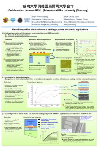
  • 1. Prof. Yonhua Tzeng Diamond and Devices Lab Department of Electrical Engineering National Cheng Kung University Diamond & Devices Lab 成功大學與德國烏爾姆大學合作 Collaboration between NCKU (Taiwan) and Ulm University (Germany) (1.) Hydrogen generation with transparent boron doped diamond (BDD) electrodes (a.) Diamond electrodes on sapphire (b.) Diamond electrodes on silicon membrane Nanodiamond for electrochemical and high power electronic applications Fabrication of electrodes on silicon  bias-enhanced nucleation (BEN)  growth of diamond films in HFCVD  E-beam lithography and thermal evaporator to form metallic clusters  etching of silicon to form diamond membrane Motivation Diamond is an electrochemically stable electrode material and is an transparent layer on a semiconductor solar cell  immerse a solar cell panel in water with gas bubbles floating off from the surface.  it does not corrode in the cathodic regime and does not form an oxide layer under anodic polarization.  neither cathodic nor anodic polarization leads to etching of diamond Modifying diamond electrodes by metallic micro dots to reduce the water splitting redox potential window (3V)  metallic clusters on diamond surface need to be stable in expected operating environments  the metallic clusters can narrow the potential window with remaining diamond electrode staying transparent Transparent diamond film  inductively coupled plasma etching  sulfur hexafluoride gas Publications Cyclic voltammetry of boron doped diamond electrode and boron doped diamond modified by titanium and platinum micro dots 0.25 % and 11% surface coverage. Narrow the potential window Enhance the current density Electrochemical measurement cluster diameter: 2 µm distance: 6 µm surface coverage: 11% Optical microscope photo Poster# P130 C. Li, Y. Tzeng, E. Kohn, M. Dipalo C.Liu, “Electrochemical and Optical Properties of Electrode with A Metallic Microdot Array on Boron Doped Diamond.” Poster# P176  Z. Gao, Y. Xu, C. Pietzka, E. Kohn, “Water Splitting with Transparent Diamond Electrodes.” (2.) Investigation of diamond nucleation -- Comparison of electrochemical activities of nanodiamond deposited on silicon with diamond seeding and bias enhanced nucleation (3.) (a) lnAIN growth on GaN at NCKU (b) Diamond seeding and growth at NCKU (c) Patterning and fabrication of HEMT at Ulm Growth temp. 750 °C Gas conc. 0.3 % CH4 in H2 Growth rate 0.12 µm/hr InAlN/GaN HEMT on sapphire - 200 nm Si3N4 passivation - standard metallization Processed in Ulm Motivation Publications Motivation BDD Intrinsic Diamond Sapphire Substrate Diamond Seeding After 500 nm growth Results Seeding with nano particles(NCKU) Fabrication of HEMT (Ulm) MOCVD growth of lnAIN/GaN on sapphire (NCKU) Device and materials analysis (Ulm and NCKU) Heat sink -4 -3 -2 -1 0 1 2 3 -20 -15 -10 -5 0 5 10 15 20 Currentdensity(mA/cm2 ) Potential vs Ag/AgCl (voltage) BDD/Ti/Pt (0.25% coverage) BDD/Ti/Pt (11% coverage) BDD No microdots 11% coverage by microdots 0.25% coverage by microdots Transmittance spectrum Diamond for heat extraction Poster# P147  Z. Gao, Y. Lin, E. Colombo, Y. Liu, Y. Tzeng, E. Kohn,“Effects of Seeding, BEN and CVD Processes on Optical Transparency of Quasi-metallically Doped NCD Electrodes Grown on Insulating Substrates.”  joint posters at 4th NDNC (New Diamond and Nano Carbons) conference in China, May 16-20, 2010 Si NCD BDD 1 μm 1 μm 500μm Si Ti Pt  Diamond films on transparent substrate are important for bio-MEMs  Deposition of Diamond films on non- diamond substrates needs seeding by nanodiamond particles or nucleation from carbide clusters (metal carbides or SiC)  Carbide clusters are not transparent but form a stable interface  Seeding by nanodiamond particles does not hinder transparency but is challenging to form a stable interface with the substrate, compromising adhesion. Contribution to existing EU-FP7 project MORGAN. Improve the cooling capability of a GaN power FET.  Thermal management of GaN power FETs by a top diamond heat spreader using NCKU seeding method for diamond layer growth. 0 2 4 6 8 10 12 0.0 0.1 0.2 0.3 0.4 0.5 0.6 -7 V LG = 0.5 痠 -6 V -5 V -2 V VDS (V) IDS (A/mm) -4 V -3 V -1 V 0 V 1 V 2 V 3 Vμm  Participation in MORGAN follow-up project proposed Prof. Erhard Kohn Materials and Devices Group Inst. of Electron Devices and Circuits Ulm University joint poster at 4th NDNC (New Diamond and Nano Carbons) conference in China, May 16-20, 2010 Acknowledgement Financial support by NSC Taiwan under the grants (NSC-98-3114-M- 006-001, NSC-96-2221-E-006-286-MY3, NSC-98-2911-I-006-031, NSC-99-2915-I-006-015) is highly appreciated. • Only Seeding (NCKU) • Seeding (NCKU) + MPCVD (NCKU) • BEN(Ulm) + MPCVD (Ulm) 1 μm nano-crystal diamond (NCD) 1 μm boron doped diamond Sapphire Substrate Diamond Seeding