This doctoral dissertation investigates the superconducting proximity effect in InAs nanowires. The first experiment observes tunneling resonances of Andreev bound states in a proximitized InAs quantum dot in the Kondo regime. An additional zero-bias peak of unknown origin is also observed. The second experiment applies an external magnetic field, revealing spin-resolved Andreev bound states in another proximitized InAs quantum dot. From the splitting of tunneling resonances, g-factors of 5 and 10 are extracted in two different devices. The third experiment compares the induced gaps of epitaxial core-shell InAs-Al nanowires with control devices using evaporated Al films. The epitaxial nanowires
![Chapter 1: Introduction
the Fermi energy. This effect, known as the superconducting proximity effect and
first observed by Holm and Meissner [1,2], offers numerous possibilities when applied
to semiconductors.
More specifically, certain combinations of superconductor and semiconductor have
received increasing interest from the condensed matter community. It has been pro-
posed that coupling superconductors to topological insulators [3–5] or materials with
high g-factor and spin-orbit coupling [6–10] can lead to exotic phases of superconduc-
tivity that may find application in topological quantum computation [11–17].
Needless to say, between being able to pass a supercurrent through a semicon-
ductor to inducing p-wave superconductivity in a semiconductor, a lot of ground has
to be covered. While experimental progress has been made by many teams over the
past few years [18–22], the truth of the matter is, less conventional semiconductors
(i.e. not Si and not GaAs) are less technologically developed, and material defects
can lead to confusing experimental signatures. Moreover, imperfect proximity effect
can cost a topological qubit its topological protection. My thesis work, hopefully a
small contributory effort to this daunting endeavor, is thus to understand some of
the fundamental characteristics of proximity effect in one of the prime semiconductor
candidates – InAs nanowires.
1.2 InAs nanowires
There are numerous advantages for using InAs nanowires. First of all, they are
known to possess the prerequisites for p-wave superconductivity – large g-factor [23]
and large Rashba spin-orbit coupling [24–29]. The small effective mass of electrons
2](https://image.slidesharecdn.com/4e276476-f8ce-40cc-b3b7-d8e360a550f9-160325143026/85/Chang_gsas-harvard-inactive_0084L_11709-18-320.jpg)
![Chapter 1: Introduction
in InAs doesn’t hurt either, because it offers a certain degree of imperviousness to
disorder. Second, they have been proven to be easily proximitized [30], most likely
due to the presence of a surface accumulation layer that reduces the potency of any
Schottky barrier between metallic leads and the surface of InAs nanowires [31, 32].
In terms of practicality, there exists an extensive library of knowledge on how to
manipulate and contact these nanowires [33]. Third, these quasi-one-dimensional
nanowires have the potential to become true one-dimensional conduction channels
[34], thereby providing another crucial ingredient for p-wave superconductivity.
What is perhaps even more attractive about InAs nanowires comes from a recent
development in materials growth by Krogstrup et al. InAs nanowires are commonly
grown via chemical vapor deposition or molecular beam epitaxy (we use nanowires
grown with the latter method). While the intrinsic structure of the nanowire crystal
can be free of stacking faults and impurities, subsequent nanofabrication on these
materials can adversely affect the quality of the nanowire. What Krogstrup et al
have managed to accomplish is to grow a layer of crystalline Al – a commonly used
superconductor – onto the InAs nanowire in situ, thereby eliminating the need to pro-
cess the surface of the nanowire before proximitizing it with superconductors. The
coherent and domain matched interface between S and N drastically enhances the
quality of the proximity effect. Moreover, because the layer of Al can be as thin as
a few nanometers, the critical parallel magnetic field of the proximitizing supercon-
ductor can be as high as 2 T [35], which, once again, satisfies another prerequisite for
inducing p-wave superconductivity in the semiconductor.
3](https://image.slidesharecdn.com/4e276476-f8ce-40cc-b3b7-d8e360a550f9-160325143026/85/Chang_gsas-harvard-inactive_0084L_11709-19-320.jpg)
![Chapter 1: Introduction
phase transition between the singlet and doublet ground states. The second is the
emergence of a zero-bias Kondo resonance at fields larger than the critical magnetic
field. The last is an additional zero-bias peak that coexists with superconductivity.
Unfortunately, the origin of the last zero-bias peak remains unresolved.
Chapter 4 continues the quantum dot story with an experiment on S-QD-N de-
vices. A few improvements were made over the previous experiment elucidated in
Chapter 3 – a higher critical magnetic field and sharper tunneling resonances. These
improvements allowed us observe spin-resolved ABSs in InAs nanowires. To the best
of my knowledge, this is the second experimental observation of spin-split ABSs after
earlier work by Lee et al in Ref. [36]. This observation allows us to directly measure
the g-factor of our InAs nanowires.
While InAs and InSb nanowires have become the favored playground for many
physicists, numerous experimental work have indicated that there remains a finite
density of states within the induced gap of these semiconductors, i.e., a soft gap.
The sought after property of topological protection in Majorana-based qubits can
only protect if the zero energy mode is decoupled from quasiparticle states by a
superconducting gap. In Chapter 5, I present experimental observations of a hard
superconducting gap in novel epitaxial core-shell InAs-Al nanowires.
In Chapter 6 I focus on a specific variety of the epitaxial core-shell InAs-Al
nanowires. When the shell covers only two or three facets of the hexagonal core,
the InAs core retains the superconducting proximity effect but is no longer shielded
by a large piece of metal from external electric fields. What this means is that it is
now possible to tune the density of states in the InAs core, and hopefully to a regime
5](https://image.slidesharecdn.com/4e276476-f8ce-40cc-b3b7-d8e360a550f9-160325143026/85/Chang_gsas-harvard-inactive_0084L_11709-21-320.jpg)
![Chapter 1: Introduction
where only a few and an odd number of sub-bands are occupied [37]. In this chapter
I present gate dependent measurements of the supercurrent, normal state resistance,
and magnetic field-dependent supercurrent interference pattern in epitaxial half-shell
InAs nanowires.
As I wrap up the last of my experiments in Chapter 6, it seems rather presumptu-
ous of me to attempt to conclude anything because I believe that these novel core-shell
nanowires mark the beginning of a wide variety of experiments. So Chapter 7 will
be spent on documenting a few experimental ideas that have been floating around
during various meetings and discussions.
Finally, Appendices A and B detail, with as much humor and panache as I can
muster upon a dry subject, the fabrication and electrical filtering techniques that
I have employed in my experiments. The appendix on fabrication techniques will
hopefully serve as a good reference for students who wish to pursue the way of InAs
nanowires. Now, without further ado, let us begin!
6](https://image.slidesharecdn.com/4e276476-f8ce-40cc-b3b7-d8e360a550f9-160325143026/85/Chang_gsas-harvard-inactive_0084L_11709-22-320.jpg)
![Chapter 2
Superconducting Proximity Effect
2.1 Introduction
The superconducting proximity effect is a phenomenon that can be elegantly de-
scribed in the language of Andreev reflection. Unfortunately, this subject is sparsely
covered by Tinkham in Introduction to Superconductivity [38], one of the most popu-
lar textbooks on superconductivity (in fact, I can see at least one copy of the textbook
on each QDev experimental setup that involves superconductors). Thankfully, there
are many tutorial and review articles on the subject that I have found incredibly
useful [39–42]. Another treasure trove of information can be found in Bretheau’s
thesis [43]. In this chapter I will briefly introduce the concepts of Andreev reflection
and relate it’s basic consequences to experimental observations in InAs nanowires.
7](https://image.slidesharecdn.com/4e276476-f8ce-40cc-b3b7-d8e360a550f9-160325143026/85/Chang_gsas-harvard-inactive_0084L_11709-23-320.jpg)
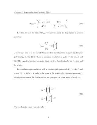
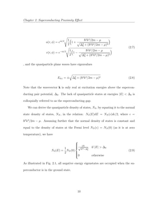
![Chapter 2: Superconducting Proximity Effect
P(E) = |B/A| = |ve/ue|, where the ratio between ve and ue is:
ve
ue
=
e−iφ
(E − sgn(E) E2 − ∆2
0)/∆0 |E| > ∆0
e−iφ
(E − i ∆2
0 − E2)/∆0 |E| < ∆0
(2.13)
arg
ve
ue
=
φ E < −∆0
φ + arccos(E/∆0) |E| < ∆0
φ + π E > ∆0
(2.14)
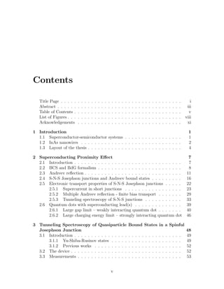
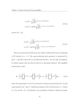
In this example, the probability of Andreev is 1 when |E| < ∆0. Andreev reflection
at energies smaller than the quasiparticle excitation gap also results in an energy
dependent phase shift of arccos(E/∆0). The energy dependent Andreev reflection
probability and its corresponding phase shift is plotted in Fig. 2.3.
(a) (b)
0.8
0.6
0.4
0.2
0.0
-3 -2 -1 0 1 2 3
E/Δ0
-3 -2 -1 0 1 2 3
E/Δ0
φ
φ π/2+
φ π+
P(E)
arg[/veue]
Figure 2.3: (a) Probability of Andreev reflection as a function of energy. Within the supercon-
ducting gap, there is perfect Andreev reflection. The reflection amplitude then drops rapidly once
|E| exceeds ∆0. (b) Phase shift due to Andreev reflection. In addition to picking up the macro-
scopic superconducting phase, the reflected electron (hole) picks up an energy dependent phase shift
arccos(E/∆0). At the Fermi level this additional phase shift is π/2.
15](https://image.slidesharecdn.com/4e276476-f8ce-40cc-b3b7-d8e360a550f9-160325143026/85/Chang_gsas-harvard-inactive_0084L_11709-31-320.jpg)
![Chapter 2: Superconducting Proximity Effect
At sub-gap energies the wavevector in the superconducting side acquires an imag-
inary part and becomes an evanescent wave. Using the Andreev approximation:
E, ∆0 µ (2.15)
we can approximate kS
e,h in Eq. 2.11 as
ke,h = kF + iσe,hκ (2.16)
κ = kF
∆2
0 − E2
µ
(2.17)
Physically, κ−1
can be interpreted as the length scale on which the evanescent wave
is damped.
The treatment of Andreev reflection at a N-S interface is greatly simplified in this
example. In a realistic system, imperfections at the interface will result in a finite
probability of specular reflection. For a full treatment of this problem, one would
have to refer to previous work by Blonder, Tinkham, and Klapwijk in Ref. [44].
2.4 S-N-S Josephson junctions and Andreev bound
states
Given that there exists a quasiparticle excitation gap, ∆, in BCS superconductors,
one can imagine trapping bound states by creating two N-S interfaces around a normal
metal. Following the example of Ref [41], let us consider the following one-dimensional
S-N-S Josephson junction illustrated in Fig. 2.4. We assume that Andreev reflection
16](https://image.slidesharecdn.com/4e276476-f8ce-40cc-b3b7-d8e360a550f9-160325143026/85/Chang_gsas-harvard-inactive_0084L_11709-32-320.jpg)
![Chapter 2: Superconducting Proximity Effect
Ψ±
e (N1) =
1
0
1
kN
e
e±ikN
e (x+L/2)
Ψ±
h (N1) =
0
1
1
kN
h
e±ikN
h (x+L/2)
(2.19)
where kN
e,h is given in Eq. (2.11) with ∆ = 0. The + (−) superscript indicates a
right (left) moving electron and a left (right) moving hole. The wavefunctions in N2
are identical once x + L/2 is replaced with x − L/2. Similarly, we can write the
wavefunctions in the superconducting region as
Ψ±
e (S1) =
ue(−φ
2
)
ve(−φ
2
)
1
kS
e
1 −
∆0
E
2 −1/4
e±ikS
e (x+L/2)
Ψ±
h (S1) =
uh(−φ
2
)
vh(−φ
2
)
1
kS
h
1 −
∆0
E
2 −1/4
e±ikS
h (x+L/2)
(2.20)
Likewise, the wavefunction in S2 is identical except for −φ/2 → φ/2 and x + L/2 →
x − L/2. The coefficients and wavevector, ue,h(φ), ve,h(φ), and kS
e,h, are defined in
Eq. (2.11).
Now that we’ve constructed the wavefunctions in each region, let us move on to
the scattering processes in the normal region and at the S-N interfaces. In the basis
of the normal wavefunctions [Eq. (2.19)], we describe the incident and scattered wave
by a vector of wave coefficients (also labelled in Fig. 2.4)
18](https://image.slidesharecdn.com/4e276476-f8ce-40cc-b3b7-d8e360a550f9-160325143026/85/Chang_gsas-harvard-inactive_0084L_11709-34-320.jpg)
![Chapter 2: Superconducting Proximity Effect
SA = e−i arccos(E/∆0)
0 0 e−iφ/2
0
0 0 0 eiφ/2
eiφ/2
0 0 0
0 e−iφ/2
0 0
(2.23)
The elements of SA are determined by matching coefficients of the wavefunctions on
the N and S sides around |x| = L/2.
Using Eqs. (2.22) and (2.23) we arrive at the condition
Ψin
N = SASN Ψin
N (2.24)
which implies that
Det(1 − SASN ) = 0 (2.25)
, where 1 is the identity matrix. After some algebra, we arrive at the expressions
Det[1 − E2
/∆2
0 − t12t∗
21 sin2
(φ/2)] = 0 (2.26)
E = ±∆0 1 − τ sin2
(φ/2) (2.27)
, where τ = t12t∗
21 is the transmission probability through the normal scatterer. The
solution describes a pair of sub-gap states which we will label |− for the ground state
(negative energy) and |+ for the excited state (positive energy). When τ = 1, the
function is 2π-periodic in phase. However, in the case of perfect transmission, the
20](https://image.slidesharecdn.com/4e276476-f8ce-40cc-b3b7-d8e360a550f9-160325143026/85/Chang_gsas-harvard-inactive_0084L_11709-36-320.jpg)
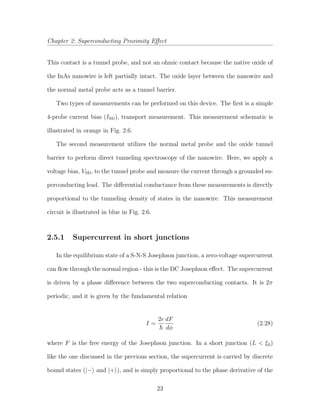
![Chapter 2: Superconducting Proximity Effect
percurrent depends on the thermal population and depopulation of the excited and
ground states, thus modifying Eq. (2.30) by a factor of [(1−f(E))−f(E)], where f is
the Fermi-Dirac distribution, f(E) = [1+exp(E/kBT)]−1
. The resultant supercurrent
is
IABS =
e∆0
2
τ sin φ
1 − τ sin2
(φ/2)
tanh
∆0
2kBT
1 − τ sin2
(φ/2) (2.31)
We can further relate the supercurrent through a Josephson junction to its nor-
mal state conductance. In the multi-channel Landauer formalism, the normal state
conductance can be expressed as
GN =
2e2
h
N
i=1
τi (2.32)
where the index i labels the transverse modes through the junction, and τi is the
individual transmission coefficient. If the normal region of a short Josephson junction
is a quantum point contact, where τi = 1 for 0 < i ≤ N and τi = 0 otherwise, Eq.
(2.31) becomes
I(φ) = GN
π∆0
e
sin(φ/2) tanh(
∆0
2kBT
cos(φ/2)) (2.33)
If, on the other hand, the normal region of the short Josephson junction is a tunnel
junction with τi 1, we can approximate Eq. (2.31) as
I(φ) =
e∆0
2
N
i=1
τi sin(φ) tanh(
∆0
2kBT
) (2.34)
Defining the critical current IC as the maximum supercurrent carried across the
25](https://image.slidesharecdn.com/4e276476-f8ce-40cc-b3b7-d8e360a550f9-160325143026/85/Chang_gsas-harvard-inactive_0084L_11709-41-320.jpg)
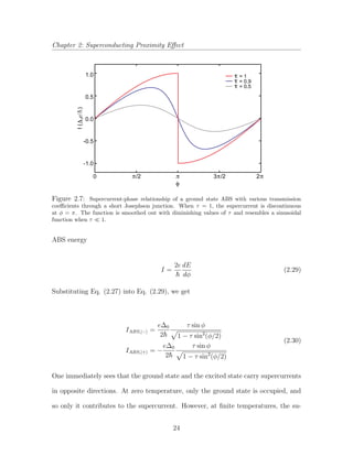
![Chapter 2: Superconducting Proximity Effect
referred to as the re-trapping current, IR. Conversely, the current at which the
junction switches from the superconducting state to a resistive state is referred to as
the switching current, IS.
In this particular example, the IV curves are acquired from positive to negative
current bias (as indicated by the arrow in Fig. 2.8). As such, IS is on the negative bias
side and IR is on the positive bias side. In principle, the switching and re-trapping
currents are not the same as the critical current of a Josephson junction. The critical
current is the theoretical limit of an ideal Josephson junction, whereas in experimental
conditions the maximum supercurrent can be reduced by electrical noise, quasipar-
ticle poisoning, and damping in the deivce. In fact, the switching and re-trapping
currents need not have the same magnitude, as in an underdamped Josephson junc-
tion, where IS > IR [38]. Nonetheless, IS is used as a crude approximation for IC in
most experiments.
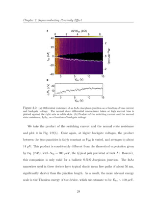
In Fig. 2.8, we see IS and IR reduce in magnitude as backgate voltage is lowered.
At the same time, the gradients of the resistive branches of the IV curves increase,
indicating a rising normal state resistances.
In Fig. 2.9(a), we show the differential resistance of the same device as a func-
tion of backgate voltage and current bias. Overlaid on the same graph, we plot the
differential conductance of the device taken at a current bias above the supercurrent
carrying branch of the Josephson junction (the data is represented by white dots and
should be read off the right vertical axis). At high backgate voltages, the differen-
tial conductance of the device tracks the switching current fairly consistently. This
agreement begins to deviate at lower backgate voltages below 4 V.
27](https://image.slidesharecdn.com/4e276476-f8ce-40cc-b3b7-d8e360a550f9-160325143026/85/Chang_gsas-harvard-inactive_0084L_11709-43-320.jpg)
![Chapter 2: Superconducting Proximity Effect
Furthermore, the opacity of the S-N interfaces can reduce the maximum supercurrent
in a Josephson junction [45]. The characteristics of diffusive versus ballistic Josephson
junctions are elaborated in greater detail in section 2.5.3. Also, considering that the
switching current is only a lower bound estimate of the true critical current, it is no
surprise that the product ISRN is widely different from ∆Al.
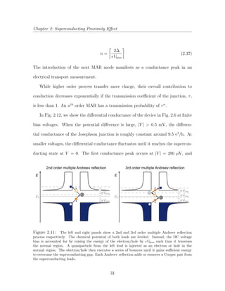
2.5.2 Multiple Andreev reflection - finite bias transport
A finite DC voltage across a Josephson junction will wind the phase difference
across the two superconducting leads in the following manner:
VDC =
2e
dφ
dt
(2.36)
It is evident then that the phase periodic supercurrent will oscillate and average to
zero, thus making no contribution to DC electronic transport.
However, the quasiparticles in the superconducting leads can participate, and a
dissipative current can flow. A quasiparticle from the left lead can tunnel into the
normal region as an electron or a hole, and the electron or hole can retro-reflect at the
two N-S interfaces multiple times while accumulating kinetic energy from the applied
voltage bias. Each reflection transfers a charge of 2e, until the electron/hole gains
enough energy to escape into the quasiparticle excitation spectrum of the supercon-
ducting leads. This process is known as multiple Andreev reflection (MAR) [46,47].
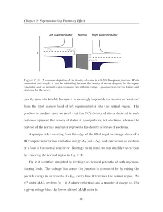
It is tempting to draw a cartoon similar to the one illustrated in Fig. 2.10, where
the superconductors have a filled ‘valence’ band and an empty ‘conduction’ band,
and the normal region has electronic states filled up to the Fermi level. However, one
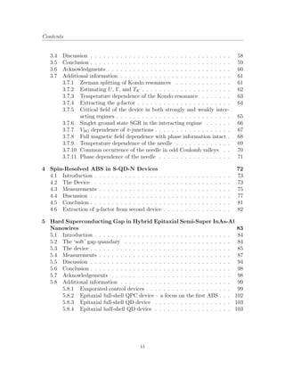
29](https://image.slidesharecdn.com/4e276476-f8ce-40cc-b3b7-d8e360a550f9-160325143026/85/Chang_gsas-harvard-inactive_0084L_11709-45-320.jpg)
![Chapter 2: Superconducting Proximity Effect
16
14
12
10
8
/dV(edI2
SD/h)
-0.6 -0.4 -0.2 0.0 0.2 0.4 0.6
V (mV)
5321 12348
Figure 2.12: Differential conductance of an InAs Josephson junction as a function of potential
difference across the junction. The first three MAR orders are recognizable as conductance peaks at
voltages values of 2∆/en, where n is an integer. Higher order processes are less visible and are not
necessarily symmetric about zero voltage.
this conductance enhancement can be interpreted as the occurrence of the 1st order
MAR. Using the relation in Eq. (2.37), we extract a superconducting pair potential of
140 µeV, and place guides (dotted vertical lines) in Fig. 2.12 to indicate the expected
positions of higher order MAR conductance peaks. We find reasonable agreement
between experiment and theory for the next two MAR orders. However, higher or-
ders of MAR are not easily identified and the differential conductance signal is not
symmetric about zero bias.
The absence of higher order peaks is expected of a disordered Josephson junction
where τ is much smaller than 1. In the case of these devices, the scattering length in
the InAs nanowire is estimated to be about 50 nm, and the junction length is 200 nm.
A much better example of MAR in nanowires was demonstrated by J. Xiang et al in
Ref. [48].
32](https://image.slidesharecdn.com/4e276476-f8ce-40cc-b3b7-d8e360a550f9-160325143026/85/Chang_gsas-harvard-inactive_0084L_11709-48-320.jpg)
![Chapter 2: Superconducting Proximity Effect
2.5.3 Tunneling spectroscopy of S-N-S junctions
In an ideal short S-N-S Josephson junction, where N is a ballistic conductor and
the S-N interfaces are perfectly transparent, the density of states in the normal region
is simple – a pair of Andreev bound states for each conduction channel, and their
energies are given by the relation in Eq. (2.27). The normal region is populated by
discrete states with energies at, or lower, than the superconductor pair potential, ∆.
However, in realistic systems, the sub-gap spectrum of the normal region is highly
dependent on a variety of factors, namely the length of the junction, the elastic mean
free path of N, and the interface transparency between S and N.
When the junction length is longer than the elastic mean free path, le, transport
through the normal region becomes diffusive. This transport regime is commonly
referred to as the ‘dirty’ limit. We can characterize diffusive transport in such a
device with its diffusion coefficient, D = levF /d, where vF is the Fermi velocity and d
is the dimensionality of the normal region. We can also define the Thouless energy of
the system, ETh = D/L2
, where L is the length of the S-N-S junction. In the dirty
limit, the S-N-S junction is best described by the quasi-classical theory developed by
Eilenberger and Usadel [49,50].
Unlike the ballistic S-N-S junction, the diffusive normal region takes on a true
excitation gap, δ [51–55]. Analogous to a superconductor, there are no electronic
states at energies within a ±δ range of the Fermi level in the normal region. This
gap is referred to as the minigap, since δ is smaller than ∆. In a diffusive Josephson
junction, the Thouless energy, instead of the pair potential of the superconducting
leads, becomes the relevant energy scale because it determines the characteristic time
33](https://image.slidesharecdn.com/4e276476-f8ce-40cc-b3b7-d8e360a550f9-160325143026/85/Chang_gsas-harvard-inactive_0084L_11709-49-320.jpg)
![Chapter 2: Superconducting Proximity Effect
for an electron to travel between the S-N interfaces. It is hence expected for δ to be
on the order of ETh.
Thus far, the discussion has been limited to short Josephson junctions (L is smaller
than the relevant phase coherence length in the system) and samples with perfect
S-N interfaces. For ballistic junctions, the relevant phase coherence length is the
superconducting phase coherence length of the leads, ξS = vF /2∆. For diffusive
junctions, one could use the energy dependent decay length, ξN = D/E. Taking
an upper limit of E = ∆, this expression is simply a geometric mean of le and ξS. Since
proximity effect originates from phase coherent Andreev reflections at S-N interfaces,
the energy scales in the sub-gap spectrum of the normal region would decay as the
length of the junction exceeds the coherence length. In addition, it has been shown
theoretically that imperfect transmission through S-N interfaces can adversely affect
the size of the minigap in a diffusive S-N-S junction [45].
Returning to the Josephson junction shown in Fig. 2.6, we engage the normal
metal tunnel probe and investigate the excitation spectrum of the proximitized InAs
nanowire. Fig. 2.13(a) shows the differential conductance of the device as a function of
voltage bias, VSD, and backgate voltage, VBG. In the tunneling limit (dI/dVSD G0 =
2e2
/h), conductance through the tunnel probe is proportional to the density of states
in the nanowire. We see that the density of states in the InAs nanowire is suppressed
at small bias voltages, consistent with theoretical expectations of a minigap around
the Fermi energy, and consistent with prior experimental work [56–58]. At higher bias
voltages, the density of states rises, then dips again around |VSD| = 200 µV. This
secondary depression, symmetric about zero-bias, marks the superconducting gap of
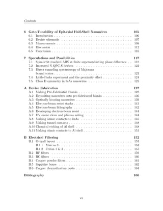
34](https://image.slidesharecdn.com/4e276476-f8ce-40cc-b3b7-d8e360a550f9-160325143026/85/Chang_gsas-harvard-inactive_0084L_11709-50-320.jpg)
![Chapter 2: Superconducting Proximity Effect
-0.4
-0.2
0.0
0.2
0.4
V(mV)SD
dI/dV(e/h)SD
2
V (V)BG
151050
0.10
0.05
V (mV)SD
dI/dV(e/h)SD
2
0.10
0.08
0.06
0.04
0.02
0.00
-0.4 -0.2 0.0 0.2 0.4
a
b
2δ
2ΔAl
Figure 2.13: (a) Tunneling differential conductance through an InAs nanowire Josephson junction
as a function of voltage bias and backgate voltage. The suppressed conductance between |VSD| = δ is
the manifestation of a minigap in the InAs nanowire. Additional conductance dips at |VSD| = 200 mV
marks the pair potential of the Al leads. (b) Differential conductance as a function of VSD, averaged
over multiple VBG values.
the Al leads.
The size of the minigap is largely independent of VBG, which tunes the chemical
potential of the nanowire. This suggests that there is a high density of electrons in
the InAs nanowire, and it can be treated as a ‘dirty’ metal. The minigap only begins
to collapse at lower backgate voltages [to the left of Fig. 2.13(a)] where the nanowire
begins to pinch-off. We average the differential conductance over multiple values of
35](https://image.slidesharecdn.com/4e276476-f8ce-40cc-b3b7-d8e360a550f9-160325143026/85/Chang_gsas-harvard-inactive_0084L_11709-51-320.jpg)
![Chapter 2: Superconducting Proximity Effect
VBG and plot the result in Fig. 2.13(b). Using the half-width of the conductance
dip around zero-bias, we estimate a minigap of 50 µeV. This value is in the same
ballpark as the estimated Thouless energy of 100 µeV. It is reasonable to expect
a less-than-perfect interface between the InAs nanowire and the Al leads, thereby
contributing to the slight discrepancy between the two values [45]. Another deviation
from theoretical expectation is the presence of a finite density of states at zero-bias.
The large amount of quasiparticle states within the minigap cannot be satisfactorily
explained by conventional theoretical models of inverse proximity effect and thermal
excitation of quasiparticles. This observation turns out to be common amongst recent
experimental systems in InAs and InSb nanowires [18–22,59]. The origin of this ‘soft’
gap, and the eventual observation of a ‘hard’ gap in InAs nanowires, is discussed in
greater detail in Chapter 5.
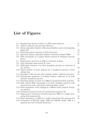
B, φ φ φ= -R L
Au
1 μmAl
Al
InAs
VSD
VBG
A
Figure 2.14: False colored SEM micrograph of an InAs Josephson junction with a normal metal
tunnel probe and superconducting phase control. The superconducting contacts are Al and the
normal metal tunnel probe is Au. The tunneling barrier is remnant native InAs oxide. A voltage
bias is applied to the tunnel probe and the resultant current through the grounded superconducting
leads is measured. Flux is applied through the 25 µm2
loop via an external perpendicular magnetic
field.
36](https://image.slidesharecdn.com/4e276476-f8ce-40cc-b3b7-d8e360a550f9-160325143026/85/Chang_gsas-harvard-inactive_0084L_11709-52-320.jpg)
![Chapter 2: Superconducting Proximity Effect
An important parameter unique to superconducting systems has been neglected
so far – the superconducting phase difference, φ, across a S-N-S Josephson junction.
In the ballistic limit, as described by Eq. (2.27), the sub-gap spectrum of the normal
region is expected to be dependent on φ. It is not unreasonable to expect a similar
phase dependence in the diffusive yet coherent transport regime. Indeed, such a
phase dependence of the diffusive minigap has been predicted [60] and subsequently
observed in proximitized Ag wires [61].
To explore the phase dependence of our InAs Josephson junctions, I introduce
another device shown in Fig. 2.14. Similar to the previous Josephson junction, a
normal metal tunnel probe contacts the InAs nanowire between two superconducting
Al leads. Instead of applying a voltage or current bias across the two superconducting
leads, the two leads are intentionally shorted together to form a loop (or rather, a
square) of area 25 µm2
. What this geometry allows is the threading of magnetic flux
through the loop, thus experimentally controlling the phase difference across the two
S-N interfaces. An external perpendicular magnetic field of 72 µT corresponds to a
reduced quantum of flux through the loop, Φ0 = h/2e, and subsequently corresponds
to a winding of phase 2π across the junction. Once again, we apply a voltage bias to
the tunnel probe and measure the differential conductance through the device in the
tunneling regime.
With no external magnetic field applied to the loop, the differential conductance
of the device as a function of VSD and VBG is shown in Fig. 2.15(a). The experimental
signature is qualitatively similar to the previous device – a suppressed density of
states at bias voltages of |VSD| < 70 µV = δ/e, and a smaller one near |VSD| =
37](https://image.slidesharecdn.com/4e276476-f8ce-40cc-b3b7-d8e360a550f9-160325143026/85/Chang_gsas-harvard-inactive_0084L_11709-53-320.jpg)
![Chapter 2: Superconducting Proximity Effect
0.7
0.6
0.5
0.4
0.3
0.2
-0.4 -0.2 0.0 0.2 0.4
0.4
a
b d
c
0.2
0.0
-0.2
-0.4
VSD(mV)
0.2
0.0
-0.2
VSD(mV)
0.4
0.2
0.0
-0.2
-0.4
VSD(mV)
VSD (mV)
32.832.632.432.232.0
VBG (V)
32.8 0 2π
φ
φ = 0
φ π=
φ = 0.0
φ π= 0.2
φ π= 0.4
φ π= 0.6
φ π= 0.8
φ π= 1.0
π 3π32.632.432.232.0
VBG (V)
0.60.40.2
dI/dV 2
SD /h)(e dI/dV 2
SD /h)(e
dI/dV2
SD/h)(e
0.50.40.30.2
Figure 2.15: (a) and (b) Differential conductance of the proximitized nanowire as a function of
VSD and VBG at φ = 0 and at φ = π respectively. (c) 2π phase periodic dependence of the minigap.
(d) Differential conductance at various phase values, averaged over multiple values in VBG.
220 µV = ∆Al/e. Parking VBG at a fixed value, we turn on a minuscule magnetic
field and measure the phase dependence of the minigap. Consistent with theoretical
expectations, the minigap closes and reopens with a periodicity of 2π [Fig. 2.15(c)].
At phase φ = π, the minigap vanishes at most backgate voltages [Fig. 2.15(b)].
Averaging across multiple values of VBG, we see in Fig. 2.15(d) that the density of
states near zero-bias returns to a value similar to the density of states at high biases
above the superconducting gap of Al. Fig. 2.15(d) also shows the averaged traces
38](https://image.slidesharecdn.com/4e276476-f8ce-40cc-b3b7-d8e360a550f9-160325143026/85/Chang_gsas-harvard-inactive_0084L_11709-54-320.jpg)
![Chapter 2: Superconducting Proximity Effect
of other phase values. The behavior of our device is qualitatively similar to earlier
experimental observations in Ag nanowires by le Sueur et al in Ref. [61].
Next, we examine the phase dependence of the secondary gap at |VSD| = 220 µV.
This secondary gap is maximal at phase φ = 0, and minimal at φ = π [see Fig. 2.15(d)],
consistent with theoretical models in Ref. [62]. Also, as theory in Ref. [63] expects,
this secondary gap is prominent when the Thouless energy of the device is similar to
the pair potential of the superconducting leads.
2.6 Quantum dots with superconducting lead(s)
Like how proximity effect modifies the continuous spectrum of a normal conductor,
the discrete spectrum of a quantum dot can take on superconducting correlations as
well. In the most naive sense, one would not be wrong to expect the proximitized
quantum dot to prefer to be occupied by an even number of electrons. However, the
picture becomes complicated once charging energy and Kondo correlations come into
play [64–67].
Following the example of Ref. [66], we can write an effective local Hamiltonian of
a quantum dot coupled to one or more superconducting leads:
Heff =
σ
d +
U
2
d†
σdσ +
U
2 σ
d†
σdσ − 1
2
− Γ(φ)(d†
↑d†
↓ + h.c.) (2.38)
Here, d is the orbital energy of the dot, U is the charging energy, dσ is the annihilation
operator of an electron on the dot with spin state σ, and Γ is the hybridization between
39](https://image.slidesharecdn.com/4e276476-f8ce-40cc-b3b7-d8e360a550f9-160325143026/85/Chang_gsas-harvard-inactive_0084L_11709-55-320.jpg)
![Chapter 2: Superconducting Proximity Effect
a = E− − E↑,↓ = U/2 − ( + U/2)2 + Γ(φ)2
b = E+ − E↑,↓ = U/2 + ( + U/2)2 + Γ(φ)2
(2.43)
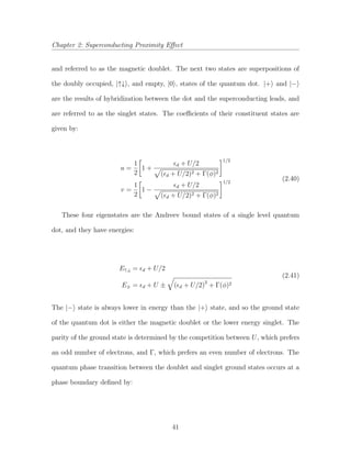
In the case of zero charging energy, the picture is very simple, and is illustrated in
Fig. 2.16. Increasing coupling to the superconducting leads increases the separation
between the symmetric tunneling resonances. Physically, the energy of the |− ground
state is lowered as hybridization with the leads increases.
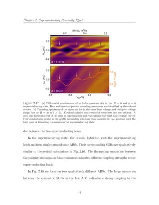
We can compare this theoretical picture with experimental observation. Returning
to the phase-controlled device in Fig. 2.14, we reduce the carrier density of the InAs
nanowire by turning down the backgate. At magnetic fields above the critical field
of the Al leads, we tune the device to a backgate region where no charging physics
is evident and the tunneling conductance smoothly varies as a function of voltage
bias and backgate voltage [Fig. 2.17(b)]. A zero-bias horizontal cut of the graph is
superimposed, and it should be read against the right axis.
The zero-bias tunneling conductance fluctuates as a function of backgate, and we
can identify four conductance peaks [indicated by colored arrows in Fig. 2.17(b)]. Four
pairs of well resolved sub-gap resonances (SGRs) emerge at these conductance peak
positions as magnetic field is turned off [Fig. 2.17(a)]. The four zero-bias conductance
peaks in the normal state of the device can be interpreted as single particle orbitals
crossing the Fermi level of the tunnel probe. The lack of Coulomb diamond resonances
and even-odd structure suggests that the charging energy is negligible, if not zero.
The InAs nanowire Josephson junction is thus occupied by a loosely confined quantum
43](https://image.slidesharecdn.com/4e276476-f8ce-40cc-b3b7-d8e360a550f9-160325143026/85/Chang_gsas-harvard-inactive_0084L_11709-59-320.jpg)
![Chapter 2: Superconducting Proximity Effect
superconducting leads [Fig. 2.18(a)]. When the single particle level is on resonance
(by tuning VBG to the point indicated by the green line), we see a strong phase
modulation of the SGRs [Fig. 2.18(b)]. Specifically, the resonances meet at zero-
bias when half a flux quantum is threaded through the superconducting loop. At
this phase value, φ = π, Andreev reflection between the two S-N interfaces interfere
destructively and reduce the hybridization of the single particle orbital to exactly zero
[for a reminder, refer to Eq. (2.43)]. This particular ABS is an example of symmetrical
coupling of the single particle level to both superconducting leads.
HighdI/dVSD (e2
/h)Low
-0.2
0.0
0.2
VSD(mV)
11.0010.95
VBG (V) φ
0 2 3π ππ
φ
0 2 3π ππ
(d) (e) (f)
4.554.50
VBG (V)
-0.2
0.0
0.2
VSD(mV)
φ
0 2 3π ππ
φ
0 2 3π ππ
(a) (b) (c)
Figure 2.18: (a) and (d) Tunneling spectrum of ABSs that are symmetrically and asymmetrically
coupled to the two superconducting leads. (b) and (e) Phase dependence of the corresponding
ABSs when VBG is on resonance with the single particle level. (c) and (f) Phase dependence of the
corresponding ABSs when they are off-resonance.
When coupling to the two superconducting leads is asymmetrical, interference
between the two Andreev reflection processes still reduces the total hybridization at
45](https://image.slidesharecdn.com/4e276476-f8ce-40cc-b3b7-d8e360a550f9-160325143026/85/Chang_gsas-harvard-inactive_0084L_11709-61-320.jpg)
![Chapter 2: Superconducting Proximity Effect
0
0
EF
E-
Δ
U < Δ U > Δ
U
0
EF
Δ
U
YSR - like singlet
(a) (b)
Figure 2.19: (a) Lowest energy states of a hybridized quantum dot with U < ∆ (large gap limit).
The first excited state is a BCS-like hybridization between the empty and doubly occupied states of
a normal quantum dot. The resultant singlet state has energy E− < U. (b) Lowest energy states
of a hybridized quantum dot in the strong interaction limit, where U > ∆. It is more energetically
favorable for the magnetic doublet ground state to form singlet correlations with quasiparticles in the
superconducting leads. This Yu-Shiba-Rusinov-like (YSR) singlet can be energetically competitive
with the magnetic doublet to become the ground state of the system.
singlet correlations with quasiparticles in the superconducting leads [68]. In other
words, the local magnetic moment in the odd parity quantum dot is screened by
quasiparticles from the leads, much like a magnetic impurity embedded in a super-
conductor as described by Yu, Shiba, and Rusinov [69–71]. This new singlet state can
have energies much lower than the superconducting gap, and modifies the conditions
for the 0 – π transition. The interplay between the quantum dot, the superconducting
leads, and Kondo correlations is the theoretical subject of many studies [64–67], and
the experimental subject of the next chapter.
47](https://image.slidesharecdn.com/4e276476-f8ce-40cc-b3b7-d8e360a550f9-160325143026/85/Chang_gsas-harvard-inactive_0084L_11709-63-320.jpg)
![Chapter 3: Tunneling Spectroscopy of Quasiparticle Bound States in a Spinful
Josephson Junction
3.1 Introduction
In this experiment, tunneling spectroscopy was performed on a segment of InAs
nanowire confined between two superconducting leads. We demonstrate both phase
and gate control of sub-gap states in a Kondo-correlated Josephson junction (kBTK ∼
∆) [72]. We also report the first evidence of a singlet to doublet QPT induced by
the superconducting phase difference. Our InAs nanowire Josephson junction has an
additional normal metal tunnel probe which allows the measurement of the density
of states via tunneling in the region between the superconducting contacts (Al).
By using normal metal, we avoid the complication of having to deconvolve the
density of states of the probe from the tunneling conductance. At magnetic fields
above the critical field of Al, tunneling into the InAs quantum dot with odd electron
occupancy showed Kondo resonances [73] with associated Kondo temperatures, TK ∼
1 K. Near zero field, tunneling into the nanowire revealed the superconducting gap
of the Al leads, ∆ 150 µeV, and a pair of sub-gap resonances (SGR) symmetric
about zero bias. For certain parameters in gate and phase, the SGRs intersect each
other at zero bias, which we interpret as a level-crossing QPT. However, no such
crossing occurred upon suppressing ∆ to zero with an applied magnetic field. Instead,
the SGRs evolve smoothly into Kondo resonances, and this transition is typically
accompanied by the appearance of a separate zero-bias resonance of unknown origin.
3.1.1 Yu-Shiba-Rusinov states
Spin impurities in superconductors can drastically modify the state of its host,
for instance, by suppressing the transition temperature and by inducing sub-gap
49](https://image.slidesharecdn.com/4e276476-f8ce-40cc-b3b7-d8e360a550f9-160325143026/85/Chang_gsas-harvard-inactive_0084L_11709-65-320.jpg)
![Chapter 3: Tunneling Spectroscopy of Quasiparticle Bound States in a Spinful
Josephson Junction
states [74]. Using a hybrid superconductor-semiconductor device, one can investi-
gate this process with precise experimental control at the level of a single impu-
rity [72]. Exchange interaction between the single quantum spin impurity and quasi-
particles modifies the order parameter locally, thereby creating Yu-Shiba-Rusinov
sub-gap states [69–71, 75, 76]. For weak exchange interaction, a sub-gap state near
the gap edge emerges from singlet correlations between the impurity and the quasi-
particles. Increasing exchange interaction lowers the energy of the singlet state and
increases a key physical parameter, the normal state Kondo temperature TK. At
kBTK ∼ ∆ (Kondo regime), where ∆ is the superconducting gap, the energy gain
from the singlet formation can exceed ∆, resulting in a level-crossing quantum phase
transition (QPT) [74, 77–79]. The QPT changes the spin and the fermion parity
of the superconductor-impurity ground state, and is marked by a peak in tunneling
conductance at zero bias [80].
A mesoscopic superconductor-quantum dot-superconductor Josephson junction
[Figs. 3.1(a) and 3.1(b)] is an ideal device to study Yu-Shiba-Rusinov states because
it provides a novel control knob that tunes the exchange interaction via the super-
conducting phase difference across the junction, φ. A physical picture of the phase
tunability of exchange interaction is the following: A spin 1/2 impurity is created by
trapping a single electron in the lowest available orbital of the dot (assuming large
level spacing) with a Coulomb barrier [Fig. 3.1(c)] [73,81]. At the electron-hole (e-h)
symmetry point, the spinful state, |1, 0 , costs less than both the empty, |0, 0 , and
the doubly occupied, |2, 0 , states by the charging energy U (U > ∆ suppresses charge
fluctuations at energies below ∆). Here, |ndot, nlead denotes the electron (quasiparti-
50](https://image.slidesharecdn.com/4e276476-f8ce-40cc-b3b7-d8e360a550f9-160325143026/85/Chang_gsas-harvard-inactive_0084L_11709-66-320.jpg)
![Chapter 3: Tunneling Spectroscopy of Quasiparticle Bound States in a Spinful
Josephson Junction
(a)
2 μm
VBG
I
VT
B,φ φ φ= -R L
(b)
Al
Al
InAs
Au
500 nm
(d)
1.
2.
3.
+φR/2
- φL/2
1.
2.
3.
(e)
+φL/2
- φR/2
(c)
Δ
S
D
SGR
0 0, 2 0,
U
Quantum Dot Right LeadLeft Lead
1 1,
1 0,
φL
φR
Figure 3.1: (a), (b) False colored scanning electron micrographs of a lithographically identical
device. (c) Lowest energy states of a single orbital quantum dot at the electron-hole symmetry point
for kBTK ∆. The states are labeled by their electron/quasiparticle occupation number in the
format |ndot, nlead . Exchange interaction dresses the states |1, 0 and |1, 1 as the doublet, |D , and
the singlet, |S , states respectively. Transition between |D and |S produces a sub-gap resonance
(SGR). (d), (e) Phase sensitive spin-flip processes coupling the |1, 1 states |↑, ↓ and |↓, ↑ via virtual
occupation of (d) |2, 0 and (e) |0, 0 .
cle) occupancies of the dot (leads), with arrows giving spin orientations when needed.
Spin-flip scattering connects the degenerate states |↑, ↓ and |↓, ↑ via the virtual pop-
ulation of states |2, 0 [Fig. 3.1(d)] or |0, 0 [Fig. 3.1(e)]. These two scattering channels
cause an effective (super-) exchange interaction between quasiparticles and the spinful
dot. Compared to scattering via |2, 0 , scattering via |0, 0 differs by a phase factor
exp(−iφ) because it is accompanied by a Cooper pair transfer [Fig. 3.1(e)]. At φ = π
these two scattering channels interfere destructively, making the exchange coupling
minimal at φ = π and maximal at φ = 0. Consequently, both the singlet excited
51](https://image.slidesharecdn.com/4e276476-f8ce-40cc-b3b7-d8e360a550f9-160325143026/85/Chang_gsas-harvard-inactive_0084L_11709-67-320.jpg)
![Chapter 3: Tunneling Spectroscopy of Quasiparticle Bound States in a Spinful
Josephson Junction
state, |S , and the doublet ground state, |D , acquire a phase modulation, albeit
only in higher order processes for the latter [64,66,67,82–86].
3.1.2 Previous works
The ground state of spinful Josephson junctions have been investigated by pre-
vious experiments [87–92]. Phase-biased junctions with weak coupling showed nega-
tive supercurrent [87,88], consistent with theoretical predictions of the weak phase-
modulation of |D [82–84], while for strong coupling, positive supercurrent was ob-
served [89, 90]. The latter was interpreted in terms of a QPT associated with the
interchange of states |S and |D at kBTK ∼ ∆ [90–92]. Meanwhile, other experi-
ments have performed tunneling spectroscopy on spinful Josephson junctions without
phase control [93–96], or with phase control but away from the Kondo regime [97].
This leaves the effect of phase on sub-gap states in the Kondo regime unaddressed.
Tunneling spectroscopy in similar devices has also been used recently to examine
signatures of Majorana end states [18–20].
3.2 The device
Epitaxially grown InAs nanowires approximately 100 nm in diameter were de-
posited on a degenerately doped Si substrate with a 100 nm thermal oxide. They
were then contacted by two ends of a superconducting loop (5/100 nm Ti/Al) with
area ∼ 25 µm2
[Figs. 3.1(a) and 3.1(b)]. For this loop area, the flux period, h/2e,
corresponds to a perpendicular magnetic field period of 72 µT. A third normal metal
tunnel probe (5/100 nm Ti/Au) contacted the nanowire at the center of the 0.5 µm
52](https://image.slidesharecdn.com/4e276476-f8ce-40cc-b3b7-d8e360a550f9-160325143026/85/Chang_gsas-harvard-inactive_0084L_11709-68-320.jpg)
![Chapter 3: Tunneling Spectroscopy of Quasiparticle Bound States in a Spinful
Josephson Junction
long junction. By adjusting ammonium polysulfide etch times, high (low) trans-
parency was achieved for the barrier between Al (tunnel probe) and InAs [33]. The
device was measured in a dilution refrigerator with a base temperature of 20 mK,
through several stages of low-pass filtering and thermalization.
3.3 Measurements
When superconductivity in the entire device was suppressed by an applied mag-
netic field, B, diamond patterns characteristic of weak Coulomb blockade (CB) were
observed in transport between the loop and the normal lead [Fig. 3.2(a)]. Consecutive
diamonds alternate in size, indicating that the orbital level spacing, ξ, is compara-
ble to the charging energy, U 200 µeV. The smaller (odd occupancy) diamonds
contain backgate-independent (VBG) zero-bias ridges that split at higher magnetic
fields (refer to Fig. 3.5) typical of the Kondo effect [73, 98]. From the temperature
dependence of the zero-bias ridges, we estimate TK to be in the range of 0.5-1 K (re-
fer to Fig. 3.7). Poor visibility of the odd diamonds suggests strong coupling to the
superconducting leads (ΓS ≥ U), and the amplitudes of the Kondo ridges indicate an
asymmetry between superconducting and normal contacts [99]. While the estimated
asymmetry, ΓN ∼ ΓS/10, will likely broaden the tunneling resonances, it is sufficient
to qualitatively treat the Au lead as a weak tunneling probe.
In the superconducting state (B ∼ 0), gap-related features were observed at
tunnel-probe voltages, VT ±150 µV ±∆/e, consistent with the gap of Al. SGRs
symmetric about zero bias were also observed [Fig. 3.2(b)]. Comparison of Figs. 3.2(a)
and 3.2(b) shows that the positioning (in VBG) of SGRs in the superconducting state
53](https://image.slidesharecdn.com/4e276476-f8ce-40cc-b3b7-d8e360a550f9-160325143026/85/Chang_gsas-harvard-inactive_0084L_11709-69-320.jpg)
![Chapter 3: Tunneling Spectroscopy of Quasiparticle Bound States in a Spinful
Josephson Junction
1.951.801.75
VBG (V)
-0.2
0.0
0.2
VT
(mV)
0.8
0.6
0.4
0.2
dI/dVT
(e2
/h)
-0.2
0.0
0.2
VT
(mV)
(a)
(b)
B ~ 0
B = 30 mT
= 0φ
2Δ
1.901.851.70
Figure 3.2: Differential conductance as a function of tunnel-probe voltage, VT, and backgate
voltage, VBG. (a) Normal state data, B = 30 mT. (b) Superconducting state data, B ∼ 0 and φ = 0.
Coulomb diamonds in (a) and superconducting gap in (b) are highlighted with dotted lines.
coincides with CB and Kondo features in the normal state. The SGRs and their
symmetric partners converge towards each other and sometimes overlap in an odd
CB valley. In contrast, they are pushed towards the gap edge in the even CB valleys.
Cuts of the data in Fig. 3.2 are shown Fig. 3.5.
Based on their qualitative dependence on VBG and φ, three categories of SGRs in
the case of a spinful dot were identified. (i) For small charging energy, U < (∆, ΓS),
SGRs do not cross the zero-bias axis for any VBG or φ [Figs. 3.3(a), 3.3(d), and 3.3(g)].
The SGR energy is maximal at φ = 0 and minimal at φ = π [Fig. 3.3(d) and 3.3(g)]—
this is the conventional phase dependence of non-interacting Josephson junctions (see
section 2.6.1). (ii) For large charging energy, U > ∆ (for estimation methods, refer to
Fig. 3.6), the SGRs overlap, crossing zero bias twice as a function of VBG [Fig. 3.3(c)].
Between zero-bias crossings, the phase dependence of SGR energies is the opposite
of the conventional behavior, that is, minimal at φ = 0 and maximal at φ = π
[Fig. 3.3(i)]. We call this a π-shifted phase dependence. Outside the intersections
54](https://image.slidesharecdn.com/4e276476-f8ce-40cc-b3b7-d8e360a550f9-160325143026/85/Chang_gsas-harvard-inactive_0084L_11709-70-320.jpg)
![Chapter 3: Tunneling Spectroscopy of Quasiparticle Bound States in a Spinful
Josephson Junction
-0.2
0.0
0.2
VT
(mV)
8.788.74
VBG (V)
dI/dVT (e2
/h)
8.82 8.86
VBG (V)
-0.90 -0.86
VBG (V)
-0.2
0.0
0.2
VT
(mV)
-0.2
0.0
0.2
VT
(mV)
0 π 2 3π π
φ
0 π 2 3π π
φ
0 π 2 3π π
φ
High Low
(a) (b) (c)
(d) (e) (f)
(g) (h) (i)
δφ
Figure 3.3: Three sub-gap resonances (SGRs) arranged in columns of increasing U. (a)–(c) VBG
dependence of the SGRs at φ = 0. The lower rows show the corresponding phase dependence off
(d)–(f) and on (g)–(i) the electron-hole symmetry point. (d)–(g) Conventional phase dependence,
(h) hybrid phase dependence, (i) π-shifted phase dependence.
in VBG, the phase dependence of SGR energy is conventional [Fig. 3.3(f)]. (iii) For
moderate charging energy U ∼ ∆ [Figs. 3.3(b), 3.3(e), and 3.3(h)], SGRs do not
intersect for any VBG at φ = 0 [Fig. 3.3(b)]. Phase dependence away from the e-h
symmetry point is conventional [Fig. 3.3(e)], but close to the symmetry point, the
pair of SGRs intersects twice per phase period of 2π [Fig. 3.3(h)]. Crossings occur at
φ = π ± δφ/2, where δφ < π is the phase difference between the two closest crossings
[Fig. 3.3(h)]. With this type of SGR, the phase dependence depends on the phase
value itself: it is conventional for φ ∼ 0, and π-shifted for φ ∼ π.
In Fig. 3.4 we examine the magnetic field evolution of three π-shifted SGRs at
55](https://image.slidesharecdn.com/4e276476-f8ce-40cc-b3b7-d8e360a550f9-160325143026/85/Chang_gsas-harvard-inactive_0084L_11709-71-320.jpg)
![Chapter 3: Tunneling Spectroscopy of Quasiparticle Bound States in a Spinful
Josephson Junction
0.5
0.4
0.3
-0.2
0.0
0.2
dI/dV(e2
/h)
3π π
φ
0 π 2
(a)
20 25100
B (mT)
200
V(mV)T
16
B (mT)
2018
T
B ~ 0
-0.2
0.0
0.2
0.3
0.2
dI/dV(e2
/h)
(g)
20 25100
B (mT)
100
(h) (i)
π3π
φ
0 π 2
V(mV)T
16
B (mT)
2018
T
0.7
0.5
0.3
-0.2
0.0
0.2
dI/dV(e2
/h)
φ
(d)
0 2π ππ- 20 25100
B (mT)
200
(f)
V(mV)T
16
B (mT)
2018
T
B ~ 0
B ~ 0
(b) (c)
= 0φ
(e)
= 0φ
Figure 3.4: Arranged in the order of decreasing TK, each row shows the evolution of a SGR at
the electron-hole symmetry point as a function of phase and magnetic field. The left column shows
phase dependence at B ∼ 0, the center column shows magnetic field dependence at φ = 0, and the
right column shows the magnetic field and phase dependence around B = 18 mT. To obtain the
phase constant panels (b) and (e), we select φ = 0 data points from the full data set. The oscillations
of the SGRs disappear abruptly at B = 19.5 mT (dotted lines) in both (c) and (f). Inset in (b) is
a closeup of the region outlined with dotted lines. A third resonance, pinned at zero bias, is clearly
visible in the high contrast color scale.
their e-h symmetry points. The first SGR [Figs. 3.4(a)–3.4(c)] is identical to the one
shown in Fig. 3.3(c). Selecting φ = 0 from the full data set shown in Fig. 3.12, the
well separated SGRs gradually approach zero-bias and merge into a Kondo resonance
in the normal state [Fig. 3.4(b)]. Temperature dependence of the normal-state Kondo
peak gives TK 1 K [73] (refer to Fig. 3.7). Taking g ∼ 13 from normal-state CB
data (refer to Fig. 3.8), the splitting of the Kondo peak at ∼ 140 mT is consistent
with this value of TK [100] [Fig. 3.4(b)]. In the other two cases (bottom two rows of
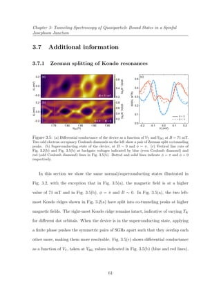
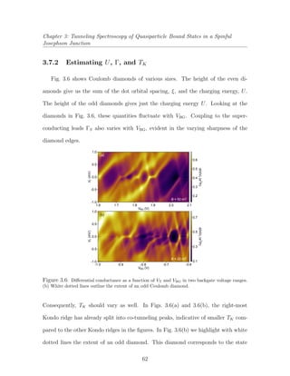
Fig. 3.4), Kondo peaks split at lower fields of B ∼ 50 mT [Fig. 3.4(e)] and B < 20 mT
[Fig. 3.4(h)], suggesting lower Kondo temperatures.
In the second case [Figs. 3.4(d)–3.4(f)], SGRs overlap at zero-bias for φ = 0, but
are separated for φ = π [Fig. 3.4(d)]. The overlapping SGRs at zero field evolve
56](https://image.slidesharecdn.com/4e276476-f8ce-40cc-b3b7-d8e360a550f9-160325143026/85/Chang_gsas-harvard-inactive_0084L_11709-72-320.jpg)
![Chapter 3: Tunneling Spectroscopy of Quasiparticle Bound States in a Spinful
Josephson Junction
continuously into a Kondo resonance as the field is increased into the normal state
regime [Fig. 3.4(e)]. Phase dependent oscillations of the SGR vanish abruptly at a
critical value of field, Bc = 19.5 mT [Fig. 3.4(f)]. The same critical field is observed
in Fig. 3.4(c), and also in higher density regimes of the device (refer to Fig. 3.9).
The last case has no phase-dependence [Fig. 3.4(g)], presumably because of poor
coupling to one of the superconducting contacts. However, its VBG dependence allows
us to establish that this SGR is indeed a π-shifted type (see Fig. 3.11). Here, in
contrast to the first two cases, the pair of SGRs evolve continuously and directly into
split Kondo peaks without ever merging or crossing at zero bias [Figs. 3.4(h) and
3.4(i)].
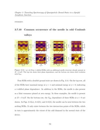
Close inspection of Fig. 3.4 reveals an unexpected and intriguing feature: a narrow
needle-like resonance pinned at zero bias. In Fig. 3.4(b), this “needle” is absent at
B = 0 but appears for B > 10 mT while the leads are still superconducting. In
Fig. 3.4(d) the needle is hidden by the SGRs at φ = 0, yet it is clearly visible at
φ = π. In this case, the needle exists at B = 0, and merges into the normal-state
Kondo resonance at higher field (most easily seen in Fig. 3.12(f) where φ = π). In
Fig. 3.4(h), the needle appears at B > 10 mT, similar to the case in Fig. 3.4(b),
despite a large difference in Kondo temperatures. In fact, the strength of the needle
appears uncorrelated with TK of the normal-state Kondo peak (see Fig. 3.13). The
needle is also distinct from the normal state Kondo resonance as seen in Figs. 3.4(h)
and 3.4(i), where three separate peaks can be identified: The two peaks flanking
the central needle appear to emerge from the SGR at the low-field end and evolve
continuously into the split Kondo peaks at the the high-field end. We find that the
57](https://image.slidesharecdn.com/4e276476-f8ce-40cc-b3b7-d8e360a550f9-160325143026/85/Chang_gsas-harvard-inactive_0084L_11709-73-320.jpg)
![Chapter 3: Tunneling Spectroscopy of Quasiparticle Bound States in a Spinful
Josephson Junction
needle only appears between the two VBG intersection points of π-shifted SGRs, which
in turn corresponds to an odd Coulomb diamond (refer to Fig. 3.14). Finally, the
needle appears brighter at φ = 0, when the separation between the two SGR is the
smallest [Figs. 3.4(c) and 3.4(d)].
3.4 Discussion
We now compare theoretical expectations for SGRs [67] to experimental observa-
tions. At the e-h symmetry point of a spinful quantum dot with suppressed charge
fluctuations, the phase-tunable exchange interaction detaches a singlet state |S down
from the gap edge [Fig. 3.1(c)]. Since quantum interference weakens the exchange
interaction at φ = π [Figs. 3.1(d) and 3.1(e)], a π-shifted SGR is indeed expected
(phase modulation of the energy of |D , being a higher-order effect, is much weaker
than that of |S ) [64,66,85,86]. This is consistent with our experiment, as seen, for
example, in Fig. 3.3(i). Strong coupling to the leads, reflected in the large TK, should
further result in a SGR that is well separated from the gap edge at φ = 0 [78, 79].
Detuning VBG towards a neighboring even diamond increases charge fluctuations and
mixes either |0, 0 or |2, 0 into |S , thereby lowering its energy. Consequently, one
expects a level-crossing QPT to a singlet ground state as VBG approaches an even
diamond, in agreement with the zero-bias crossings in Fig. 3.2(b) and Fig. 3.3(c).
This QPT is predominantly governed by the enhanced charge fluctuations away from
the e-h symmetry point. Finally, the observed conventional phase dependence in the
even state of the dot [Fig. 3.3(f)] is also expected, because a spinless dot effectively
acts as a potential scatterer in a non-interacting junction [101].
58](https://image.slidesharecdn.com/4e276476-f8ce-40cc-b3b7-d8e360a550f9-160325143026/85/Chang_gsas-harvard-inactive_0084L_11709-74-320.jpg)
![Chapter 3: Tunneling Spectroscopy of Quasiparticle Bound States in a Spinful
Josephson Junction
A more interesting QPT occurs in Fig. 3(h) as a function of phase-bias. It corre-
sponds to a situation where the energy gain from the quasiparticle-dot singlet forma-
tion makes this state the ground state at φ = 0 but not at φ = π. This behavior is
known in theory literature as 0 -junction or π -junction [67,102], and, to our knowl-
edge, has not been reported in previous experiments.
Reducing ∆ sufficiently below kBTK should result in a level-crossing QPT that
is driven entirely by spin fluctuations [74]. Experimentally, we would see a zero-bias
crossing of the SGRs at B < Bc as B is increased to suppress ∆. However, this theo-
retical expectation is not seen in our device as exemplified in Figs. 3.4(b) and 3.4(h),
perhaps obscured by our current experimental resolution or by the needle feature. The
needle may be related to similar features observed in recent experiments [95,96]. An
unlikely soft gap in Al may explain such a resonance in terms of conventional Kondo
screening. We note, however, that the needle itself does not split with increasing B,
as one might expect from a conventional Kondo effect. More intriguingly, the needle
appears much stronger at φ = 0 than at φ = π, suggesting possible phase dependence
and a link to the sub-gap states (refer to Fig. 3.15). While the observed behaviors
of sub-gap states agree at B ∼ 0 with existing theory on Yu-Shiba-Rusinov states,
further theory and experiment are needed to understand the origin of the needle and
the magnetic field dependence of the sub-gap states [65,103].
3.5 Conclusion
In summary, tunnel-probe spectroscopy of the density of states of an InAs quan-
tum wire with controlled phase between two superconducting contacts is realized
59](https://image.slidesharecdn.com/4e276476-f8ce-40cc-b3b7-d8e360a550f9-160325143026/85/Chang_gsas-harvard-inactive_0084L_11709-75-320.jpg)
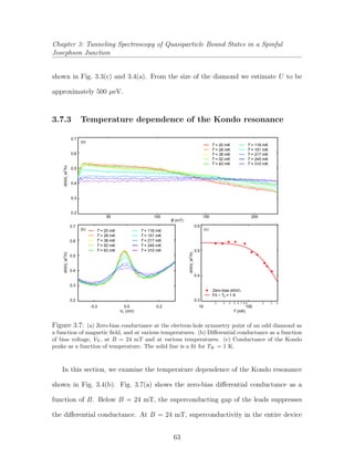
![Chapter 3: Tunneling Spectroscopy of Quasiparticle Bound States in a Spinful
Josephson Junction
is fully removed, and the differential conductance reaches its maximum value. As
B is increased, the Kondo resonance diminishes in amplitude and eventually splits,
resulting in the decrease of the differential conductance. Taking the differential con-
ductance at its maximal value when B = 24 mT, we plot it as a function of VT at
various temperatures in Fig. 3.7(b). We then fit the zero-bias differential conductance
with the following expression from Ref. [104]:
G(T) = G0{1 + (21/s
− 1)(T/TK)2
}−s
(3.1)
, where s = 0.22 for spin 1/2 electrons and G0 and TK are fit parameters. The result
is an estimated Kondo temperature of TK = 1 K.
3.7.4 Extracting the g-factor
To extract the g-factor of our InAs nanowire device, we reduce VBG until the
device is almost pinched off. Sharply defined Coulomb diamonds and their excited
states indicate that the device is in the deep Coulomb blockade regime [Fig. 3.8(a)].
Fixing the backgate voltage at the value indicated by the green line in Fig. 3.8(a), we
examine the voltage bias and magnetic field dependence of these tunneling resonances
in Fig. 3.8(b). The ground state of the dot splits linearly in magnetic field [dotted lines
in Fig. 3.8(c)]. Taking the value of the splitting and correcting for the capacitance of
the leads, we extract a g-factor of 13.
64](https://image.slidesharecdn.com/4e276476-f8ce-40cc-b3b7-d8e360a550f9-160325143026/85/Chang_gsas-harvard-inactive_0084L_11709-80-320.jpg)
![Chapter 3: Tunneling Spectroscopy of Quasiparticle Bound States in a Spinful
Josephson Junction
-4.60 -4.55 -4.50 -4.45
VBG (V)
60
40
20
0
0.40.20.10
B (T)
40
20
0
1.0
0.8
0.6
0.4
0.2
0.0
0.40.30.20.10
B (T)
40
20
0
-4
-2
0
2
4
VT(mV)
-4
-2
0
2
4
VT(mV)
dI/dVT(10
-3
e
2
/h)
dI/dVT(10
-3
e
2
/h)
0.3
VT(mV)
dI/dVT(10
-3
e
2
/h)
B = 0 mT
(a) (b)
(c)
Figure 3.8: (a) Differential conductance as a function of VT and VBG in the deep Coulomb blockade
regime. (b) Taking a cut of (a) at a fixed VBG (green line) and examining the magnetic field
dependence. (c) A closeup of the Zeeman split resonance in (b).
3.7.5 Critical field of the device in both strongly and weakly
interacting regimes
We compare the magnetic field dependence of the device in two different regimes -
strongly interacting and weakly interacting. In the strongly interacting case [Fig. 3.9(a)],
we show the full magnetic and flux dependence of a SGR with a π-shifted phase de-
pendence [same SGR shown in Fig. 3.4(d)–(f)]. Similar data is shown in Fig. 3.9(b)
for a SGR in the weakly interacting regime. Unlike the SGR in Fig. 3.9(a), no Kondo
resonance in the normal state is observed. Comparing their zero-bias conductance
in Fig. 3.9(c), oscillations due to the phase dependent SGRs vanish abruptly at a
65](https://image.slidesharecdn.com/4e276476-f8ce-40cc-b3b7-d8e360a550f9-160325143026/85/Chang_gsas-harvard-inactive_0084L_11709-81-320.jpg)
![Chapter 3: Tunneling Spectroscopy of Quasiparticle Bound States in a Spinful
Josephson Junction
0.8
0.6
0.4
0.2
Weakly interacting
0.7
0.6
0.5
0.4
0.3
dI/dVT(e2
/h)
-0.2
0.0
0.2
VT(mV)
20151050
B (mT)
0.7
0.6
0.5
0.4
0.3
-0.2
0.0
0.2
VT(mV)
dI/dVT(e2
/h)
dI/dVT(e2
/h)
(a)
(b)
(c)
Strongly interacting
Strongly interacting π
Regular phase relation
- shifted phase relation
Weakly interacting
Figure 3.9: (a) Magnetic field dependence of a SGR in the strongly interacting regime. A Kondo
zpeak appears above the critical magnetic field. (b) Magnetic field dependence of an SGR in the
weakly interacting regime. (c) Zero-bias conductance cuts as a function of B. Oscillations stop
abruptly at B = 19.5 mT.
common magnetic field B = 19.5 mT. This magnetic field value is also common for
all charge configurations, and it is treated as the critical field, Bc of the device.
3.7.6 Singlet ground state SGR in the interacting regime
Fig. 3.10 illustrates an example where exchange interaction is large enough such
that the ground state is a YSR-like singlet. The SGRs do not intersect at φ = 0
for any value of VBG [Fig. 3.10(a) and 3.10(d)], and their phase dependence at the
e-h symmetry point is regular [Fig. 3.10(b)]. At higher fields, the SGRs merge into a
Kondo resonance that subsequently splits [Fig. 3.10(c)]. Away from the e-h symmetry
66](https://image.slidesharecdn.com/4e276476-f8ce-40cc-b3b7-d8e360a550f9-160325143026/85/Chang_gsas-harvard-inactive_0084L_11709-82-320.jpg)
![Chapter 3: Tunneling Spectroscopy of Quasiparticle Bound States in a Spinful
Josephson Junction
π
dI/dV(e2
/h)
-π
φ
0 π 2
(a)
(d)
(b)
(e)
π-π
φ
0 π-2
-0.2
0.0
0.2
V(mV)T
-0.2
0.0
0.2
V(mV)T
1000 50 200150
B (mT)
(c)
(f)
TdI/dV(e2
/h)T
0.7
0.5
0.3
0.8
0.6
0.4
1.0
0.6
0.2
dI/dV(e2
/h)T
-0.2
0.0
0.2V(mV)T
-0.2
0.0
0.2
V(mV)T
1.0
0.6
0.2
dI/dV(e2
/h)T
1000 50 200150
B (mT)
5.35.2
VBG (V)
5.35.2
VBG (V)
B ~ 0
B ~ 0
B ~ 0
B ~ 0
= 0φ
= 0φ
Figure 3.10: (a) and (d) SGR with a singlet ground state at φ = 0. (b) and (c) Phase dependence
and magnetic field dependence of the SGR at the electron-hole symmetric point. (e) and (f) Phase
and magnetic field dependence of the SGR away from the odd diamond.
point [green line in Fig. 3.10(d)], the phase dependence of the SGR is still regular,
but at higher fields the Kondo resonance is absent.
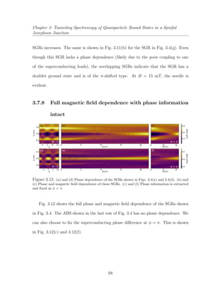
3.7.7 VBG dependence of π-junctions
-0.2
0.0
0.2
VT(mV)
-0.44 -0.42 -0.40
VBG (V)
0.80.60.40.2
dI/dVT (e2
/h)
-0.14 -0.12 -0.10
0.2 0.4
dI/dVT (e2
/h)
VBG (V)
B ~ 0 B = 15 mT= 0φ
(a) (b)
Figure 3.11: (a) and (b) VBG dependence of the SGR shown in Fig. 3.4(d) and Fig. 3.4(g)
respectively.
VBG dependence of the SGR in Fig. 3.4(a) is shown in Fig. 3.3(c). Fig. 3.11(a)
shows VBG dependence of the SGR in Fig. 3.4(d). At φ = 0, the SGRs are just
touching at zero-bias. When φ is shifted away from 0, the overlap between the two
67](https://image.slidesharecdn.com/4e276476-f8ce-40cc-b3b7-d8e360a550f9-160325143026/85/Chang_gsas-harvard-inactive_0084L_11709-83-320.jpg)
![Chapter 3: Tunneling Spectroscopy of Quasiparticle Bound States in a Spinful
Josephson Junction
3.7.9 Temperature dependence of the needle
We examine the temperature dependence of the needle shown in Fig. 3.4(a)–(c).
Fig. 3.13(a)–(f) shows the magnetic field dependence of the SGR at six different
temperatures. Phase information is removed and fixed at φ = 0 so that the needle is
clearly visible. We notice in Fig. 3.13(d) that when T = 52 mK, the needle becomes
indiscernible from the surrounding SGRs. Taking cuts in VT at B = 13 mT, we see
that a small zero-bias peak is visible for temperatures up to 52 mK. This is plotted
in Fig. 3.13(g) and then offset vertically in Fig. 3.13(h) for better clarity. Keeping
in mind that the Kondo temperature for this feature is about 1 K, we note here the
difference in energy scales of the needle when compared to the normal state Kondo
0.45
0.40
0.35
dI/dVT(e
2
/h)
-0.2
0.0
0.2
VT(mV)
-0.2
0.0
0.2
VT(mV)
-0.2
0.0
0.2
VT(mV)
2015105
B (mT)
2015105
B (mT)
dI/dVT(e
2
/h)
0.45
0.40
0.35
0.30
dI/dVT(e
2
/h)
0.45
0.40
0.30
0.25
0.35
-0.2 0.0 0.2
VT
(mV)
-0.1 0.1
T = 20 mK
T = 28 mK
T = 38 mK
T = 52 mK
T = 83 mK
T = 116 mK
T = 20 mK
T = 28 mK
T = 38 mK
T = 52 mK
T = 83 mK
T = 116 mK
B = 13 mT
B = 13 mTT = 20 mK T = 28 mK
T = 38 mK T = 52 mK
T = 83 mK T = 116 mK
= 0φ
= 0
= 0
= 0
= 0= 0
φ
φ
φ
φ
φ
(a) (b)
(c) (d)
(e) (f)
(g)
(h)
Figure 3.13: (a) - (f) VT and B dependence of the SGR and needle at six temperatures. (g)
Vertical cuts [green lines in (a) - (f)] at B = 13 mT. (h) The same data that is shown in (g), except
that they are offset vertically for better clarity.
69](https://image.slidesharecdn.com/4e276476-f8ce-40cc-b3b7-d8e360a550f9-160325143026/85/Chang_gsas-harvard-inactive_0084L_11709-85-320.jpg)
![Chapter 3: Tunneling Spectroscopy of Quasiparticle Bound States in a Spinful
Josephson Junction
3.7.11 Phase dependence of the needle
0.5
0.4
0.3
dI/dVT(e
2
/h)
20151050
B (mT)
0.5
0.4
0.3
-0.2 0.0 0.2
0.5
0.4
0.3
0.2
-0.2
0.0
0.2
VT(mV)
-0.2
0.0
0.2
VT(mV)
-0.2 0.0 0.2
dI/dVT(e
2
/h)dI/dVT(e
2
/h)
VT (mV) VT (mV)
B = 12.5 mT
= 0φ
π=φ
B = 15 mT
= 0φ
π=φ
B = 20 mT
= 0φ
π=φ
B = 0 mT
= 0φ
π=φ
(a)
(b)
(c) (d)
(e) (f)
= 0φ
π=φ
Figure 3.15: (a) and (b) Phase extracted magnetic field dependence of the needle at phases 0 and
π respectively. (c)–(f) Cuts in bias voltage for each phase at four different magnetic fields.
In this section we look into the possible phase dependence of the needle. In
Fig. 3.15(a) and 3.15(b) we compare the magnetic field dependence of the needle at
phases 0 and π. Compared on the same vertical color scale, we see that the needle
is more visible at a lower magnetic field when φ = 0. Taking cuts in VT at four
different values of B, we compare the effects of φ on the needle. At B = 12.5 mT
[Fig. 3.15(c)], the zero-bias peak is visible at φ = 0 but absent at φ = π. At B = 15 mT
[Fig. 3.15(d)], a strong zero-bias peak can be seen at φ = 0, and a fainter one at φ = π.
The feature is missing at B = 0 mT [Fig. 3.15(e)] for both phases, and at B = 20 mT
the traces are identical [Fig. 3.15(f)].
71](https://image.slidesharecdn.com/4e276476-f8ce-40cc-b3b7-d8e360a550f9-160325143026/85/Chang_gsas-harvard-inactive_0084L_11709-87-320.jpg)
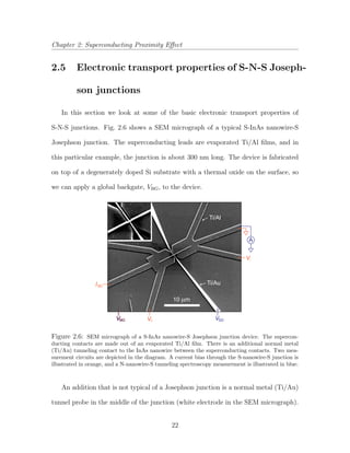
![Chapter 4: Spin-Resolved ABS in S-QD-N Devices
4.1 Introduction
In the previous experiments, the critical field of the devices were limited to about
20 mT. Assuming a g-factor of 10 for InAs, any Zeeman splitting of the sub-gap
resonances (SGRs) would be smaller than 10 µeV. Compounded with broadened
tunneling resonances, it becomes obvious that these devices are ill-suited for direct
measurements of the spin and magnetic properties of QD-S systems.
In this chapter, I turn to a different set of devices fabricated on InAs-Al core-shell
nanowires. While the critical field of these devices are only slightly improved (Bc
ranges from 80 mT to 250 mT), the vastly sharpened tunneling resonances allows us
to distinguish Zeeman split SGRs.
We observe the Zeeman splitting of the magnetic doublet Andreev bound state
(ABS) and extract g-factors ranging from 5 to 10. The experimental observations are
largely consistent with theoretical expectations, with the exception that we occasion-
ally observe an extra pair of spin-split SGRs when the ground state of the QD is a
magnetic doublet. To the best of our knowledge, this is the second tunneling spec-
troscopy observation of spin-split ABS in InAs nanowires after prior experimental
work in Ref. [36].
4.2 The Device
The InAs-Al core-shell nanowires used in these devices are grown epitaxially in
a molecular beam epitaxy chamber. After growing the InAs core axially, Al is then
grown radially around the core in situ. This results in a pristine and impurity free
73](https://image.slidesharecdn.com/4e276476-f8ce-40cc-b3b7-d8e360a550f9-160325143026/85/Chang_gsas-harvard-inactive_0084L_11709-89-320.jpg)
![Chapter 4: Spin-Resolved ABS in S-QD-N Devices
I
VSD
B
BGV
SGV
1 μm
Figure 4.1: False color SEM micrograph of a lithographically similar device. Yellow represents the
normal metal leads (Au), green the InAs core, and gray the superconducting shell and leads (Al). A
source drain bias voltage, VSD, is applied to the normal metal lead and we measure the differential
conductance across the device. Voltage applied to the backgate, VBG, or sidegate, VSG, tunes the
density of states of the exposed InAs core.
S-N interface. Further details on these core-shell nanowires can be found in Ref. [35]
and also in Chapter 5. We deposit these nanowires on a degenerately doped Si
substrate with a 100 nm thermal oxide. To expose the InAs core, we used ‘Aluminum
etchant - Type D’, manufactured by Transene Company Inc. (details can be found in
Appendix A.10). The electrodes are defined with standard electron beam lithography
techniques. To make ohmic contacts to the Al shell and InAs core, the native oxides
on the nanowire are removed with Ar ion milling prior to metals deposition. The core
is contacted with a normal metal lead (Ti/Au, 5/80 nm), and the shell is contacted
with a superconducting lead (Ti/Al, 5/130 nm). A lithographically similar device
is shown in Fig. 4.1. The chemical potential of the exposed core can be tuned via
a sidegate, VSG, or the backgate, VBG. We find that a QD forms naturally in the
74](https://image.slidesharecdn.com/4e276476-f8ce-40cc-b3b7-d8e360a550f9-160325143026/85/Chang_gsas-harvard-inactive_0084L_11709-90-320.jpg)
![Chapter 4: Spin-Resolved ABS in S-QD-N Devices
region of the exposed InAs core – a common feature of nanowire devices. The device
is measured in a dilution refrigerator with a base temperature of 20 mK. In order to
maximize the magnitude of the critical magnetic field, we apply the external magnetic
field along the length of the nanowire.
4.3 Measurements
Using a combination of VBG and VSG, we bring the device into the tunneling regime
(G G0 = 2e2
/h). As illustrated in Figs. 4.2(a) and 4.2(c), SGRs can be seen in the
middle of odd Coulomb valleys, and they can be readily identified as ABSs arising
from discrete QD levels. In Fig. 4.2(a), the pair of SGRs at zero magnetic field
splits into four distinct resonances at B = 40 mT. Tuning VSG to the particle-hole
symmetry point of the Coulomb diamond, we look at the magnetic field dependence of
the resonances in Fig. 4.2(b). The SGRs split linearly in B, until the superconducting
gap closes and the resonances wash out into the background (Bc ∼ 70 mT).
Fig. 4.2(c) shows an ABS with a magnetic doublet ground state at the particle-hole
symmetry point. The crossing of resonances at zero-bias indicates a QPT between
singlet and doublet ground states. Like the ABS shown in Fig. 4.2(a), the pair of SGRs
split into four distinct resonances at finite magnetic fields. However, the doubling of
resonances does not occur everywhere along VSG. In fact, there is only one pair of
SGRs near the middle of the Coulomb valley. Tuning VSG away from the particle-hole
symmetry point and away from the QPTs, the resonances once again split linearly in
B [Fig. 4.2(d)].
Fig. 4.3 shows a rather peculiar ABS at B = 40 mT. It is superficially similar
75](https://image.slidesharecdn.com/4e276476-f8ce-40cc-b3b7-d8e360a550f9-160325143026/85/Chang_gsas-harvard-inactive_0084L_11709-91-320.jpg)
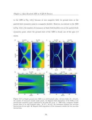
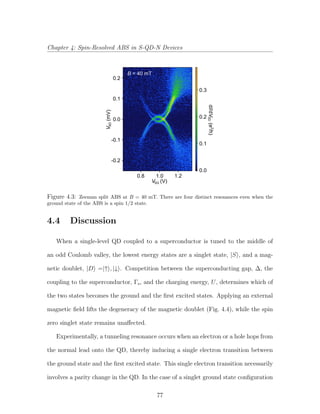
![Chapter 4: Spin-Resolved ABS in S-QD-N Devices
[Fig. 4.4(a)], the degeneracy of the first excited state, the magnetic doublet, is lifted
linearly as the magnetic field is increased. Because both spinful states are individually
odd and the singlet state has even parity, a single electron transition is allowed from
the singlet ground state to both spin 1/2 states. Therefore, at finite fields, what was
originally one single tunneling resonance now becomes two. This picture is consistent
with our observations shown in Fig. 4.2(a) and 4.2(b). In Fig. 4.2(a), the ABS
remains in the singlet ground state throughout the Coulomb valley. As expected,
the number of resonances also doubles throughout the gate voltage range of the ABS
at finite magnetic fields. At the particle-hole symmetry point, the linear splitting
of the resonance is a measure of the Zeeman energy between the two spin states,
EZ = µBgB. From Fig. 4.2(b), we extract a g-factor of approximately 10. The
experimental observations of a singlet ABS from a second device is also consistent with
B
E
SGR
SGR
S
D
B
E
SGR
S
D
Singlet ground state Magnetic doublet ground statea b
Figure 4.4: Lowest energy states of a S-QD system in the presence of an external magnetic field.
(a), Singlet ground state configuration. Single electron transition from the ground state to both
spin 1/2 states are allowed. (b) Doublet ground state configuration. When the degeneracy is lifted,
a transition is only allowed between the lower energy spinful state (ground state) and the excited
singlet state.
78](https://image.slidesharecdn.com/4e276476-f8ce-40cc-b3b7-d8e360a550f9-160325143026/85/Chang_gsas-harvard-inactive_0084L_11709-94-320.jpg)
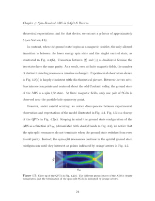
![Chapter 4: Spin-Resolved ABS in S-QD-N Devices
This effect is even more pronounced in the ABS shown in Fig. 4.3, where four
distinct resonances exist throughout the entire gate voltage range of the ABS. These
observations seemingly contradict the experimental results of Lee et al in Ref. [36],
where the more energetic spin-split resonances stops abruptly at the gate voltage
QPTs.
We suggest a possible mechanism for the additional resonances by carefully exam-
ining the intermediate configuration of lowest energy states between what is illustrated
in Fig 4.4(a) and 4.4(b). When a singlet or a doublet ground state is near the QPT
point in gate voltage space, additional Zeeman energy can result in a state config-
uration illustrated in Fig. 4.6, where the two spin 1/2 states sandwich the singlet
state. Like the example in Fig. 4.4(b), the only allowed direct transition is between
the |↑ ground state and the |S first excited state. However, provided that the bias
voltage is sufficient, it is possible to execute a double transition from |↑ to |↓ via
the |S state since each transition changes the parity of the QD occupancy (the first
and second transitions are indicated by the gray and blue arrows in Fig. 4.6). The
double transition mechanism offers a second current path through the QD and thus
registers as a second resonance in the tunneling differential conductance.
The double transition is allowed until a level crossing occurs between |S and |↓ ,
the more energetic spin 1/2 state, which happens as the gate voltage is tune towards
the particle-hole symmetry point. The points at which this occurs in VSG is indicated
in Fig. 4.5 by orange arrows. When the singlet state becomes the most energetic state,
the only current carrying transition is between |↑ and |S , thus only one tunneling
resonance remains. This expectation is consistent with the termination point of the
80](https://image.slidesharecdn.com/4e276476-f8ce-40cc-b3b7-d8e360a550f9-160325143026/85/Chang_gsas-harvard-inactive_0084L_11709-96-320.jpg)
![Chapter 4: Spin-Resolved ABS in S-QD-N Devices
B
E
SGR
S
D
Double transition
Figure 4.6: Lowest energy states of a hybridized QD near the QPT point. When |S is sand-
wiched between |↑ and |↓ , a double transition is allowed to happen between the two spin states by
temporarily populating the singlet state (gray and blue arrows).
more energetic spin-split resonance in Figs. 4.2(c) and 4.5.
While the double transition is possible, we note that it becomes increasingly un-
likely as Zeeman energy grows and the level separation becomes larger. This might
explain the absence of an additional tunneling resonance in the observations of Lee
et al in Ref. [36]. Their reported Zeeman splitting between the two spin 1/2 states is
on the order of 100 µeV, while the Zeeman splitting in our devices at B = 40 mT is
on the order of 10 µeV.
4.5 Conclusion
In summary, we observed Zeeman split tunneling resonances of ABS in QD-S
devices. The tunneling spectrum of our devices is consistent with our theoretical
expectations, and we suggest a possible higher order transition to explain the dis-
81](https://image.slidesharecdn.com/4e276476-f8ce-40cc-b3b7-d8e360a550f9-160325143026/85/Chang_gsas-harvard-inactive_0084L_11709-97-320.jpg)
![Chapter 4: Spin-Resolved ABS in S-QD-N Devices
crepancies between our experimental observations and those reported in Ref. [36].
4.6 Extraction of g-factor from second device
-0.2
-0.1
0.0
0.1
0.2
VSD(mV)
VBG (V)
-0.2
-0.1
0.0
0.1
0.2
VSD(mV)
2.352.30
VBG (V)
2.352.30
0.8
0.6
0.4
0.2
0.0
GS(e2
/h)GS(e2
/h)
4003002001000
B (mT)
0.5
0.4
0.3
0.2
0.1
0.0
B = 0 B = 100 mT
a
b
Figure 4.7: Device B. a, Singlet ground state ABS. The pair of resonances split into four distinct
resonances at B = 100 mT. b, Magnetic field dependence of the resonances at the particle-hole
symmetry point.
Fig. 4.7 shows a singlet ABS in a second InAs N-QD-S device. At B = 100 mT,
the pair of symmetrical SGRs splits into two sets. At the particle-hole symmetry
point, we examine the tunneling resonances as a function of VSD and B. Because
of the higher critical field of this device, the spin-split resonances are more readily
resolved in Fig. 4.7(b). From this dataset, we extract a g-factor of approximately 5.
82](https://image.slidesharecdn.com/4e276476-f8ce-40cc-b3b7-d8e360a550f9-160325143026/85/Chang_gsas-harvard-inactive_0084L_11709-98-320.jpg)
![Chapter 5: Hard Superconducting Gap in Hybrid Epitaxial Semi-Super InAs-Al
Nanowires
5.1 Introduction
In this chapter, we present measurements of hard induced superconducting gap
in epitaxially grown InAs-Al core shell nanowires. These hybrid nanowires come
in two flavors, the first having a core that is completely covered by Al (full-shell),
and the second having a core that is only half covered (half-shell). Both nanowire
types display strong superconducting proximity effect in the InAs core, with sub-gap
conductances up to two orders of magnitude lower than its normal state value. In
addition, we find the conductance of the half-shell type to be gate dependent. The
robust proximity effect, the hardness of the induced gap, and the gate-tunability of
these hybrid nanowires make them an attractive platform on which induced p-wave
superconductivity can be experimentally investigated.
5.2 The ‘soft’ gap quandary
The predicted existence of Majorana bound states in exotic phases of superconduc-
tivity [6] has garnered widespread attention because of their potential applications in
topological quantum computation [9,13–17]. Proposals to create a topological p-wave
superconducting state by coupling a regular s-wave superconductor to a semicon-
ducting nanowire with strong spin-orbit coupling and large g-factor are particularly
alluring because the required ingredients are readily available [7,8]. While zero-bias
conductance peaks in tunneling spectroscopy measurements have been reported by
numerous experiments on InAs and InSb nanowires [18–22,59], a common experimen-
tal observation is the presence of a large amount of sub-gap density of states. The
84](https://image.slidesharecdn.com/4e276476-f8ce-40cc-b3b7-d8e360a550f9-160325143026/85/Chang_gsas-harvard-inactive_0084L_11709-100-320.jpg)
![Chapter 5: Hard Superconducting Gap in Hybrid Epitaxial Semi-Super InAs-Al
Nanowires
origin of this soft gap is unknown, and theoretical models have attributed its exis-
tence to interface roughness between semiconductor and superconductor [105], and to
the inverse proximity effect of the normal metal tunneling probe [106]. On a grander
scale, the soft gap represents a serious obstacle in the efforts to realize nanowire-
based Majorana qubits because quasiparticle poisoning can nullify the highly coveted
property of topological protection [107,108].
5.3 The device
The InAs cores of the nanowires were grown axially in the wurzite [0001] direc-
tion with molecular beam epitaxy (MBE) [109]. After reaching lengths of 5–10 µm,
Al was then grown radially around the core in situ. The resulting semiconductor-
superconductor interface, shown in Fig. 5.1(c), is coherent, domain matched, and
impurity free. Further details on the nanowire bicrystal growth can be found in
Ref. [35]. Full-shell nanowires are completely covered by Al [Fig. 5.1(a)], while half-
shell nanowires are only in contact with Al on two or three facets of the hexagonal core
[Fig. 5.5(a)]. The core-shell (40 nm core diameter, 40 nm shell thickness) nanowires
were deposited on a degenerately doped Si substrate with a 100 nm thermal oxide.
We contacted the shell with a superconducting Ti/Al (5/130 nm) lead and the core
with a normal metal Ti/Au (5/80 nm) lead. To expose the InAs core, an etchant
that selectively targets Al was used. All contacts to the nanowire were made highly
transparent by ion-milling away the native oxides in situ before metal deposition.
Fig. 5.1(d) shows a SEM micrograph of a lithographically similar device.
To compare the quality of the induced superconducting gap between an epitaxi-
85](https://image.slidesharecdn.com/4e276476-f8ce-40cc-b3b7-d8e360a550f9-160325143026/85/Chang_gsas-harvard-inactive_0084L_11709-101-320.jpg)
![Chapter 5: Hard Superconducting Gap in Hybrid Epitaxial Semi-Super InAs-Al
Nanowires
6
4
2
0
(10G-22
/h)e
GS/GN
0.01
0.1
1
10
a b
d
e f
c InAs Al
-0.4 -0.2 0.0 0.40.2
V (mV)SD
-0.4 -0.2 0.0 0.40.2
V (mV)SD
B
BGV
SGV
VSD
InAs
Al
Epi
Evap
Epi
Evap
B = 0
B > Bc
1 μm
I
Figure 5.1: Epitaxial full-shell device with a hard induced gap a, Cross-section schematic
of an epitaxial full-shell nanowire. b, Measurement set-up. Yellow represents normal metal (Au),
green InAs, and gray superconductor (Al). c, TEM image of epitaxial N-S interface. d, False colored
SEM micrograph of a lithographically similar device. e, Differential conductance as a function of
source-drain voltage of an epitaxial full-shell device (blue) and an evaporated control device (red).
Solid lines represent data at zero magnetic field while dashed lines represent data at fields above
the critical magnetic field, Bc. f, Normalized differential conductance. Epitaxial full-shell nanowires
exhibit a sub-gap conductance suppression of up to two orders of magnitude.
ally defined N-S interface and an evaporated N-S interface, we separately fabricated
control devices using similar nanowires. In these devices, the entirety of the shell was
removed with Al etchant. We replaced the shell with evaporated Al in select areas
to create a device similar to its epitaxial counterpart [Figs. 5.1(b) and 5.1(d)], with
86](https://image.slidesharecdn.com/4e276476-f8ce-40cc-b3b7-d8e360a550f9-160325143026/85/Chang_gsas-harvard-inactive_0084L_11709-102-320.jpg)
![Chapter 5: Hard Superconducting Gap in Hybrid Epitaxial Semi-Super InAs-Al
Nanowires
the exception that the underside of the InAs core is in contact with the substrate
and not Al. We found it necessary to introduce a 5 nm Ti sticking layer between
the nanowire and the evaporated Al film in these control devices because numerous
devices fabricated without the sticking layer showed poor induced gap and a highly
disordered sub-gap spectrum (see section 5.8.1). We thus compare gap measurements
from epitaxial full-shell and half-shell devices against control devices proximitized
via an evaporated Ti/Al (5/50 nm) ‘half-shell’. The measurement schematic for all
devices is shown in Fig. 5.1(b). The carrier density in the exposed core can be tuned
with a sidegate voltage, VSG, or a backgate voltage, VBG. In this experiment, we
use only the backgate. Unless stated otherwise, the external magnetic field, B, was
applied parallel to the length of the nanowire. All measurements were performed in
a dilution refrigerator with a base temperature of 20 mK.
5.4 Measurements
We first bring the devices into a tunneling regime (G G0 = 2e2
/h) by reducing
VBG. The tunneling spectrums of an epitaxial full-shell device (blue) and an evap-
orated device (red) are shown in Fig. 5.1(e). In the superconducting state (B = 0)
both devices exhibit peaks in differential conductance at symmetrical source-drain
voltages, VSD. Between these two peaks, conduction is suppressed. The peaks and
dip disappear as we increase B above the critical magnetic field, Bc (∼75 mT for
epitaxial full-shell and ∼250 mT for evaporated control). In the normal state, both
devices show similar tunneling conductances of approximately 0.01 e2
/h [dashed lines
in Fig. 5.1(e)]. We refer to the differential conductance in the B = 0 superconducting
87](https://image.slidesharecdn.com/4e276476-f8ce-40cc-b3b7-d8e360a550f9-160325143026/85/Chang_gsas-harvard-inactive_0084L_11709-103-320.jpg)
![Chapter 5: Hard Superconducting Gap in Hybrid Epitaxial Semi-Super InAs-Al
Nanowires
state as GS, and the differential conductance in the B > Bc normal state as GN. In
Fig. 5.1(f), we compare the normalized tunneling conductance (GS/GN) of the two
devices. The epitaxial full-shell device shows an induced gap of ∆∗
= 190 µeV, similar
to the superconducting gap of bulk Al, and a sub-gap conductance suppression of up
to two orders of magnitude. The evaporated control device shows a smaller induced
gap of 140 µeV, and a sub-gap conduction suppressed by at best a factor of 5, similar
to reported experiments in proximitized InAs and InSb nanowires [18–22,59].
Increasing VBG increases both sub and above-gap conductances of the epitaxial
full-shell device. A pair of sub-gap resonances (SGR) appears close to the gap edge in
the range -11 V < VBG < -8 V [Fig. 5.2(a)]. The appearance of this SGR coincides with
a sharp increase in the above-gap conductance. The rest of the tunneling spectrum
is devoid of other SGRs. In this device, no evidence of dot-like charging physics was
observed [Fig. 5.2(b)]. Conductance peaks independent of VBG occur at VSD = 190 µV,
and in some areas the sub-gap conductance exceeds the normal state conductance.
This sub-gap conductance enhancement is illustrated in Fig. 5.2(c), which shows two
vertical cuts taken at low and high backgate voltages [indicated by orange and green
lines in Figs. 5.2(a) and 5.2(b)]. In Fig. 5.2(d) we plot the superconducting zero-bias
conductance as a function of conductance at VSD = 0.4 mV. On the same graph,
we plot, with no free parameter, the theoretical dependence between GS(VSD = 0)
and GN(VSD = 0), given by the following expression in Blonder-Tinkham-Klapwijk-
Beenakker (BTKB) theory [44,110]
GS VSD=0
= 2G0
G2
N
(2G0 − GN)2
(5.1)
88](https://image.slidesharecdn.com/4e276476-f8ce-40cc-b3b7-d8e360a550f9-160325143026/85/Chang_gsas-harvard-inactive_0084L_11709-104-320.jpg)
![Chapter 5: Hard Superconducting Gap in Hybrid Epitaxial Semi-Super InAs-Al
Nanowires
VSD(mV)
-0.4
-0.2
0.2
0.4
0.0 0 2 4 6 8 100.2 0.4 0.6 0.8
0.0
-12
0.1
0.01
10.1
-10 -10 -5 0 5 10-8
G (e2
S /h) G (e2
S /h)
VBG (V) VBG (V)
VSD(mV)
0.0
0.5
-0.5
1.0
-1.0
G (e
2
S
(0.4mV)
/h)
G(e2
S
(0)/h)
2Δ*/e
a
c
e
d
b
BTKB Theory
Experiment
VSD (mV)
-0.4 -0.2 0.2 0.40.0
2
0 5
15
4
6
Ge(102-2
S/h)
G(e2
S/h)
G(e2
S/h)
16
12
8
4
0
20100-10
VBG (V)
(mT)B
0.0
0.0
0.5
0
0
100
(mV)VSD
VBG (V)
-12.0
3.8
Figure 5.2: Conductance of a ballistic one-dimensional N-S junction in an epitaxial full-
shell device. a, b, Differential conductance of a full-shell device as a function of backgate, VBG,
and VSD. c, Vertical cuts of a and b in the tunneling (orange), and open (blue) regimes. d Zero-
bias versus finite-bias (0.4 mV) conductance. The solid line (red) represents the theoretical relation
between the two quantities. e, Conductance steps as a function of VBG at zero-bias, above-gap bias,
and normal state (B = 100 mT > Bc).
The device also exhibits conductance steps as a function of VBG [Fig. 5.2(e)], a
typical signature of quantum point contacts (QPC). Zero-bias conductance in the
89](https://image.slidesharecdn.com/4e276476-f8ce-40cc-b3b7-d8e360a550f9-160325143026/85/Chang_gsas-harvard-inactive_0084L_11709-105-320.jpg)
![Chapter 5: Hard Superconducting Gap in Hybrid Epitaxial Semi-Super InAs-Al
Nanowires
0.60.40.20.0
GS (e2/h)
-1.0 -0.8 -0.6 -0.4 -0.2
VBG (V)
-0.4
-0.2
0.0
0.2
0.4
VSD(mV)
-0.4 0.0 0.4
VSD (mV)
0.3
0.2
0.1
0
GS(e/h)2
-0.4 0.0 0.4
VSD (mV)
5
6
4
3
2
1
0
GS/GN
QPC
QD
a b
c d
QD
QPC
2Δ*
2Δ*
Odd
Even
Figure 5.3: Epitaxial full-shell quantum point contact vs quantum dot devices. a,
Tunneling spectrum of a proximitized InAs core coupled to a QPC (upper panel) and QD (lower
panel). b, Andreev bound states in a quantum dot. The green (orange) line indicates the particle-
hole symmetry point of an even (odd) Coulomb diamond. c, Vertical cuts of b. d, Comparison of
tunneling measurements between a QPC device and a QD device in an even valley.
normal state (black line) shows plateaus at values close to 1, 3, 6, and 10 e2
/h. In the
superconducting state and at source-drain bias above ∆∗
/e (red line), the device con-
ductance shows a similar behavior, but the begins to deviate above 6 e2
/h. Plateaus
are less defined at zero-bias in the superconducting state (green line). Instead, con-
ductance oscillates around the normal state values and peaks on the lower VBG edge
of the normal state plateaus.
Not all of the measured devices, epitaxial or evaporated, form QPCs. Instead, a
quantum dot (QD) can form in the exposed InAs core [Fig. 5.3(a)]. In the normal
90](https://image.slidesharecdn.com/4e276476-f8ce-40cc-b3b7-d8e360a550f9-160325143026/85/Chang_gsas-harvard-inactive_0084L_11709-106-320.jpg)
![Chapter 5: Hard Superconducting Gap in Hybrid Epitaxial Semi-Super InAs-Al
Nanowires
state of an epitaxial full-shell QD device, Coulomb diamond resonances and well de-
fined even-odd structures can be identified (see supplementary information). In the
superconducting state, symmetric SGRs in the shape of inverted bells occupy the odd
diamond valleys [Fig. 5.3(b)]. These SGRs, arising from Andreev bound states (ABS)
or Yu-Shiba-Rusinov states (YSR) [69–71,75,76], have been extensively investigated
in previous studies [36, 59, 64, 66, 93–95, 97]. Similar QD structure and their asso-
ciated SGRs in the superconducting state are also observed in our control devices.
Vertical cuts at the particle-hole symmetry point of an odd (orange) and even (green)
Coulomb valley are shown in Fig. 5.3(c). Away from the SGRs, both even and odd
Coulomb valley traces show highly suppressed sub-gap conductances. We compare
the normalized conductance of an epitaxial full-shell QPC device against an epitaxial
full-shell QD device tuned to the middle of an even Coulomb valley [Fig. 5.3(d)]. The
two measurements are almost indistinguishable, and this experimental observation
allows us to compare induced gap measurements between various devices, regardless
of their QPC or QD nature. Since fabricated QPC devices are of a rarer variety than
QD devices in nanowire systems, all comparisons between epitaxial and evaporated
devices are between the epitaxial full-shell QPC device and an evaporated QD device.
In Figs. 5.4(a) and 5.4(b) we study the evolution of the induced gap as a func-
tion of magnetic field and temperature. We then compare the normalized zero-bias
conductance of an epitaxial full-shell device against an evaporated control device in
Figs. 5.4(c) and 5.4(d). Since the sub-gap conductance in epitaxial devices is close
to our experimental noise-floor, we average over a 40 µV window centered about
zero-bias and define this value as G
(0)
S /G
(0)
N . Experimental error bars smaller than
91](https://image.slidesharecdn.com/4e276476-f8ce-40cc-b3b7-d8e360a550f9-160325143026/85/Chang_gsas-harvard-inactive_0084L_11709-107-320.jpg)
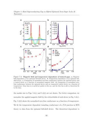
![Chapter 5: Hard Superconducting Gap in Hybrid Epitaxial Semi-Super InAs-Al
Nanowires
a b
dc
e
1 μm
BGV
BiasI
InAs
Al
V
6
4
2
0
GS/GN
-0.4 0.0 0.4
V (mV)SD
V (mV)BG
cB= 100mT >
GWire GShell+
50
-10 0 10 20 30
40
30
20
10
0
G(e2
/h)
Full
Half
B
GShell
B
Figure 5.5: Epitaxial half-shell device and gate-tunability of InAs core a, Cross-section il-
lustration of a half-shell nanowire. b Gate-tunability measurement schematic of a half-shell nanowire
device. c, Comparison of induced gap quality between an epitaxial full-shell and half-shell device.
d, SEM micrograph of a lithographically similar device. e, conductance of the Al shell and InAs
core as a function of VBG.
given by the expression [38]
GS
GN VSD=0
=
2π∆∗
kBT
e−∆∗/kBT
(5.2)
, where kB is the Boltzmann constant and T is the temperature. From the theoretical
fit (blue line), we extract an induced gap of 160 µeV.
We fabricate similar devices on epitaxial half-shell nanowires [Figs. 5.5(a), 5.5(b),
93](https://image.slidesharecdn.com/4e276476-f8ce-40cc-b3b7-d8e360a550f9-160325143026/85/Chang_gsas-harvard-inactive_0084L_11709-109-320.jpg)
![Chapter 5: Hard Superconducting Gap in Hybrid Epitaxial Semi-Super InAs-Al
Nanowires
and 5.5(d)], with the exception that an additional Al lead is added to the device, and
these leads now contact both the shell and the core. Identical tunneling spectroscopy
is performed on these devices, and we compare the induced gap quality of the full-
shell QPC device to a half-shell QD device in Fig. 5.5(c). The induced gap size of
an epitaxial half-shell device (180 µeV) is similar to the induced gap size in epitaxial
full-shell devices. The normalized sub-gap conductance is a factor of 50 lower than the
normal state conductance, substantially better than the induced gap in evaporated
control devices.
The additional Al lead to the shell allows us to explore the gate-tunability of the
half-exposed InAs core. As illustrated in Fig. 5.5(b), we apply a current bias between
the two Al leads and measure the voltage drop when the device is in the normal
state (B⊥ = 100 mT > Bc). Conductance through the normal state Al shell and the
semiconducting InAs core is shown in Fig. 5.5(e). It remains roughly constant at 10
e2
/h below VBG = 3 V, then rises to approximately 45 e2
/h at much higher VBG.
5.5 Discussion
Normalized sub-gap conductance suppression of up to two orders of magnitude rep-
resents a significant improvement in the hardness of induced gaps in InAs nanowires
[19,21,59,94]. This number should be regarded as a lower bound limited by the experi-
mental noise floor of our measurement set-up [Fig. 5.1(f)]. While we cannot isolate the
effects of a Ti sticking layer on the hardness of the proximitized gap, we note that our
control devices fabricated without the sticking layer have produced far inferior induced
gaps. The collective measurements across multiple devices, epitaxial and evaporated,
94](https://image.slidesharecdn.com/4e276476-f8ce-40cc-b3b7-d8e360a550f9-160325143026/85/Chang_gsas-harvard-inactive_0084L_11709-110-320.jpg)
![Chapter 5: Hard Superconducting Gap in Hybrid Epitaxial Semi-Super InAs-Al
Nanowires
suggests that the soft gap is a result of semiconductor-superconductor interface rough-
ness [105]. Commonly practiced methods of proximitizing these nanowires require the
removal of native oxides either via chemical etching or physical ion-milling before the
deposition of a superconducting metal. These fabrication steps can potentially dam-
age the crystalline semiconductor surface.
Interface quality aside, the QPC nature of our epitaxial full-shell device demon-
strates ballistic transport in the semiconducting core. The only SGR present in the
QPC device [Fig. 5.2(a)] coincides in VBG with the the first conductance plateau in the
normal state. We interpret this resonance as an ABS formed from the first sub-band
of a one-dimensional channel [41].
In the tunneling limit, we approximate the normal state conductance by the
quasiparticle transport conductance measured at sufficiently high source-drain bias
(VSD = 0.4 mV > ∆∗
/e). Comparing this value against the zero-bias superconduct-
ing state conductance, we find excellent agreement between experiment and BTKB
theory [44, 110] [Fig. 5.2(d)]. What is remarkable is that the comparison between
experiment and theory has no free parameter. The zero-bias superconducting state
conductance of a single channel N-S junction depends solely on the transmission coef-
ficient, τ, which, in Landauer formalism, is directly proportional to the normal state
conductance. Measurement noise notwithstanding, the striking similarity between
experiment and theory tells us that the hardness of the induced gap is close to its
theoretical limit.
Further agreement with BTKB theory can be found by comparing sub-gap con-
ductances between the tunneling regime and the open transport regime [Fig. 5.2(c)].
95](https://image.slidesharecdn.com/4e276476-f8ce-40cc-b3b7-d8e360a550f9-160325143026/85/Chang_gsas-harvard-inactive_0084L_11709-111-320.jpg)
![Chapter 5: Hard Superconducting Gap in Hybrid Epitaxial Semi-Super InAs-Al
Nanowires
At low backgate voltages, the probability of Andreev reflection [111] is low because
of a high tunnel barrier [Fig. 5.3(a), upper panel] between the normal lead and the
proximitized InAs core [44]. At high backgate voltages, the barrier is lowered and
the sub-gap conductance is enhanced above its normal state value. However, we note
that there remains a finite probability for an electron to specular reflect against the
proximitized core. This is evident from the fact that the sub-gap conductance never
reaches twice its normal state value.
Conductance steps as a function of backgate voltage are evident in Fig. 5.2(e), but
the steps do not occur at typical QPC values. The discrepancy could be attributed
to imperfect transmission of one-dimensional conduction modes [112] and additional
symmetries in the transverse confining potential of the nanowire [113]. In addition,
while we have subtracted line resistances from our measurement set-up, we cannot
account for additional contact resistances within the device.
While QPCs and QDs represent vastly different transport regimes in a nanowire,
both types of devices allow us to perform tunneling spectroscopy on the proximitized
core. As illustrated in Fig. 5.3(a), a QPC near pinch-off forms a single tunnel barrier
between the normal electrode and the InAs core. On the other hand, a single QD
can be envisioned as two tunnel barriers with discrete states in between. Since the
charging energy of the reported QD device is larger than the induced gap ∆∗
, when
VBG is tuned to the particle-hole symmetry point of an even Coulomb diamond, the
discrete QD states are far from the edge of the induced gap. The QD thus acts as a
single tunnel barrier between the normal lead and the proximitized InAs core. The
agreement of tunneling spectroscopy measurements between the QPC and the QD
96](https://image.slidesharecdn.com/4e276476-f8ce-40cc-b3b7-d8e360a550f9-160325143026/85/Chang_gsas-harvard-inactive_0084L_11709-112-320.jpg)
![Chapter 5: Hard Superconducting Gap in Hybrid Epitaxial Semi-Super InAs-Al
Nanowires
device [Fig. 5.3(c)] serves as an experimental validation of this interpretation.
In Figs. 5.4(a) and 5.4(c), we note that the floor of the induced gap remains
close to zero, rising sharply only when B approaches Bc. Retaining a hard gap at
finite magnetic fields is an important trait for Majorana bound state experiments
since theoretical framework requires that the Zeeman energy in the semiconductor be
larger than the induced s-wave pairing gap [6–8]. While the temperature dependent
tunneling conductance from BCS theory [38] qualitatively fits our experimental ob-
servation [Fig. 5.4(d)], the extracted induced gap of 160 µeV does not coincide with
our tunneling spectroscopy measurement of ∆∗
= 190 µeV. Alternatively, one can in-
terpret this discrepancy as an effective device temperature that is roughly a factor of
1.2 larger than the measured temperature of the dilution refrigerator. Although the
actual electron temperature can be higher than the cryostat temperature, we expect
the two values to agree fairly well at elevated temperatures above 100 mK.
Turning our attention to the epitaxial half-shell variety of nanowires, we find that
the induced gap has similar hardness to their full-shell cousins [Fig. 5.5(c)]. More
interestingly, in the normal state of the Al shell, the conductance between the two Al
leads is gate-dependent. The resistance saturates at about 2.5 kΩ below VBG = 3 V,
and lowers to about 600 Ω at higher backgate voltages [Fig. 5.5(e)]. We interpret
the saturated resistance to be the resistance of the Al shell, and the subsequent
reduction of resistance to come from the opening of a parallel conduction channel
through the InAs core. Using the capacitance model from Ref. [114], we estimate the
following transport parameters for the InAs core: (i) carrier density (at high VBG),
n = 5 × 10¹⁸
cm−3
(ii) mobility, µ = 3300 cm2
/Vs (iii) elastic scattering length,
97](https://image.slidesharecdn.com/4e276476-f8ce-40cc-b3b7-d8e360a550f9-160325143026/85/Chang_gsas-harvard-inactive_0084L_11709-113-320.jpg)
![Chapter 5: Hard Superconducting Gap in Hybrid Epitaxial Semi-Super InAs-Al
Nanowires
le = 100 nm. These are typical values for InAs nanowires reported in Refs. [115,116].
However, the expected resistance for our Al shell should be on the order of 101
Ω.
The higher measured resistance could be attributed to additional contact resistance
between the Al leads and the Al shell.
5.6 Conclusion
While epitaxial full-shell nanowires provide interesting geometries (cylindrical su-
perconducting shell) for future experiments, it is probably the epitaxial half-shell va-
riety that strongly interests the Majorana community. The possibility of controlling
the sub-band occupation in a large spin-orbit, large g-factor quasi-one-dimensional
semiconductor while maintaining a hard induced superconducting gap makes the epi-
taxial half-shell nanowire an ideal platform for nanowire-based Majorana qubits.
5.7 Acknowledgements
We thank N. L. B. Ziino, and K. Flensberg for fruitful discussions. Support was
received from Microsoft Project Q, the Danish National Research Foundation, the
Carlsberg Foundation, the Villum Foundation, and the Lundbeck Foundation.
98](https://image.slidesharecdn.com/4e276476-f8ce-40cc-b3b7-d8e360a550f9-160325143026/85/Chang_gsas-harvard-inactive_0084L_11709-114-320.jpg)
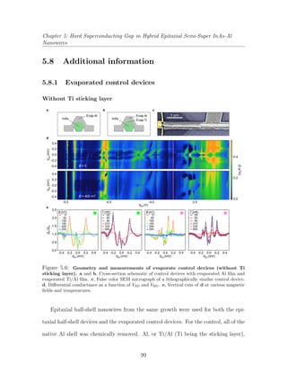
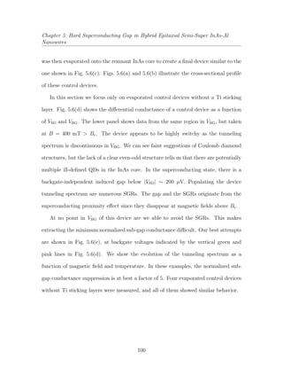
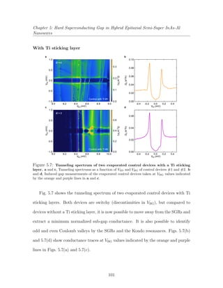
![Chapter 5: Hard Superconducting Gap in Hybrid Epitaxial Semi-Super InAs-Al
Nanowires
5.8.2 Epitaxial full-shell QPC device – a focus on the first
ABS
Additional data on the single ABS in the epitaxial full-shell QPC device is shown
in Fig. 5.8. Data shown in Fig. 5.8(a) is identical to data shown in Fig. 5.2(a). Here,
we change the aspect ratio to place emphasis on the ABS. Fig. 5.8(b) shows the
evolution of the induced gap and the ABS as a function of magnetic field. The ABS
remains close to the gap edge, then merges into the continuum above B ∼ 40 mT.
It shows up most prominently as two peaks in an one-dimensional trace taken at
VBG = -10 V [Fig. 5.8(c)].
-0.3
-0.2
-0.1
0.0
0.1
0.2
0.3
a b c
V(mV)SD
V (mV)SDV (mV)BG B (mT)
-0.2
-0.1
0.0
0.1
0.2
V(mV)SD
G(e/h)S
2
G (e /h)S
2
-11 -10 -9 0 20 40 60 80
0.80.60.40.20.0
G (e /h)2
0.60.40.20.0
0.8
0.6
0.4
0.2
0.0
-0.4 -0.2 0.0 0.2 0.4
B = 0
Figure 5.8: ABS of the first sub-band in the epitaxial full-shell QPC device. a, Tunneling
spectrum below the first conductance plateau. A pair of horizontal SGRs can be seen at the edge
of the induced gap. b, Magnetic field dependence of the SGRs. c, Vertical cut of a (orange line),
showing two small conductance peaks at the edge of the induced gap.
102](https://image.slidesharecdn.com/4e276476-f8ce-40cc-b3b7-d8e360a550f9-160325143026/85/Chang_gsas-harvard-inactive_0084L_11709-118-320.jpg)
![Chapter 5: Hard Superconducting Gap in Hybrid Epitaxial Semi-Super InAs-Al
Nanowires
5.8.3 Epitaxial full-shell QD device
We turn our attention to measurements from epitaxial full-shell QD devices. Dis-
tinct Coulomb diamond resonances with charging energy on the order of 1 meV can
be seen in Fig. 5.9. Furthermore, even-odd structure can be seen from the presence
of both Kondo resonances (normal state) and SGRs (superconducting state) in every
other Coulomb diamond. QD data shown in Fig. 5.3(d) is taken at the particle-
hole symmetry point of an even Coulomb diamond [indicated by the pink line in
Fig. 5.9(a)].
-3
-2
-1
0
1
2
3
VSD(mV)
B = 0
0.8
1.0
0.6
0.4
0.2
0.0
(eG2
S/h)
VBG (V)
-0.8 -0.6 -0.4 -0.2 0.0 0.2
-3
-2
-1
0
1
2
3
VSD(mV)
(eG2
N/h)
VBG (V)
-0.8 -0.6 -0.4 -0.2 0.0 0.2
0.6
0.4
0.2
0.0
B = 100 mT
a b
Figure 5.9: Charge stability diagram of an epitaxial full-shell QD device. a and b,
Differential conductance as a function of VSD and VBG at B = 0 and B = 100 mT respectively. Pink
line in a indicates the backgate voltage at which the induced gap measurements shown in Figs. 5.3(c)
and 5.3(d) is taken.
5.8.4 Epitaxial half-shell QD device
Three epitaxial half-shell QD devices were measured. In Figs. 5.10(a) and 5.10(b)
we show the charge stability diagrams of one of the devices at zero and at finite
magnetic fields. The QD nature of this device is evident from Coulomb diamonds,
103](https://image.slidesharecdn.com/4e276476-f8ce-40cc-b3b7-d8e360a550f9-160325143026/85/Chang_gsas-harvard-inactive_0084L_11709-119-320.jpg)
![Chapter 5: Hard Superconducting Gap in Hybrid Epitaxial Semi-Super InAs-Al
Nanowires
c
-2
-1
0
1
2
VSD(mV)
VBG (V)
2.22.01.81.6
1.0
0.8
0.6
0.4
0.2
0.0
GS(e2
/h)
a
B = 0
-2
-1
0
1
2
VSD(mV)
VBG (V)
2.22.01.81.6
0.3
0.2
0.1
0.0
GN(e2
/h)
b
B = 350 mT
-0.4
-0.2
0.0
0.2
0.4
VSD(mV)
GS(e2
/h)
2.01.91.81.71.61.5
1.0
0.8
0.6
0.4
0.2
0.0
VBG (V)
B = 0
Figure 5.10: Charge stability diagram of an epitaxial half-shell QD device. a and b,
Charge stability diagram of the device at B = 0 and B > Bc. Coulomb diamonds with charging
energy on the order of 1 meV are evident. In the normal state, a spin-split Kondo resonance occurs
near VBG = 2.2 V. c, Close-up of the sub-gap spectrum in the backgate voltage range of a and b;
numerous SGRs are visible. The pink line indicates the backgate voltage value at which the induced
gap measurement shown in Fig. 5c is taken.
and its charging energy is on the order of 1 meV. In the normal state [Fig. 5.10(b)], we
see a pair of spin-split Kondo resonances near VBG = 2.2 V. In the superconducting
state, the Kondo resonance turns into a pair of SGRs [Fig. 5.10(a)]. To extract
a measurement of the induced gap, we move away from the SGRs in VBG. Data
shown in Fig. 5.5(c) is taken at a backgate voltage value indicated by the pink line
in Fig. 5.10(c).
104](https://image.slidesharecdn.com/4e276476-f8ce-40cc-b3b7-d8e360a550f9-160325143026/85/Chang_gsas-harvard-inactive_0084L_11709-120-320.jpg)
![Chapter 6: Gate-Tunability of Epitaxial Half-Shell Nanowires
6.1 Introduction
One of the key criteria to induce a topological phase in a super-semi hybrid struc-
ture is to be able to tune the chemical potential of the one dimensional semiconductor
into the induced superconducting gap. Furthermore, the number of occupied sub-
bands must be odd in order for the zero-energy Majorana mode to manifest [6–10,37].
It was unclear if this was experimentally feasible, because proximitizing semiconduct-
ing nanowires usually involved placing large pieces of superconductors on top of, and
in good contact to, the target semiconductor. The presence of a metal could screen
the effectiveness of gate electrodes, and the good contact to a metal could potentially
dope the semiconductor and increase its carrier density.
In the previous chapter, we saw that the normal state (B > Bc) conductance of a
segment of an epitaxial half-shell nanowire varies as a function of backgate voltage,
VBG. In this chapter, we further investigate the superconducting properties of these
epitaxial half-shell nanowires as a function of VBG and magnetic fields in various
directions.
In addition to a gate-dependent normal state resistance, we observe that the max-
imum supercurrent carried by the S-nanowire-S Josephson junction varies with VBG.
The maximum supercurrent also varies as a non-monotonic function of applied mag-
netic field – a signature similar to Fraunhofer interference in Josephson junctions.
From the local minima (in magnetic field) of the supercurrent, we extract an effec-
tive area of the Josephson junction. The calculated effective cross-sectional areas of
the Josephson junction are consistent with the lithographic dimensions of the device.
Moreover, the areas diminish as VBG is reduced.
106](https://image.slidesharecdn.com/4e276476-f8ce-40cc-b3b7-d8e360a550f9-160325143026/85/Chang_gsas-harvard-inactive_0084L_11709-122-320.jpg)
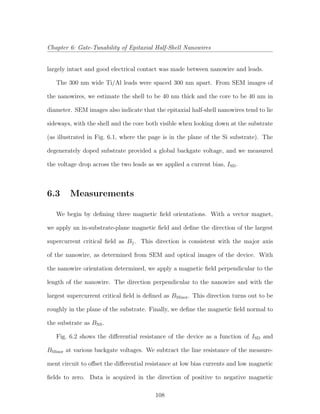
![Chapter 6: Gate-Tunability of Epitaxial Half-Shell Nanowires
-100
-50
0
50
100
(nA)SDI
-200 -100 0 100 200
BMinor (mT)
-200 -100 0 100 200
BMinor (mT)
-200 -100 0 100 200
BMinor (mT)
86420
(kSD ΩdV/dI )
86420
(kSD ΩdV/dI )
6420
(kSD ΩdV/dI )
VBG = 35 V VBG = 0 V VBG = -35 V
Figure 6.2: Differential resistance of the hybrid Josephson junctions as a function of current bias
and BMinor at three different backgate values. The resistance in the normal state and the size of the
maximum supercurrent increases and decreases respectively with a decreasing backgate voltage.
field and negative to positive current bias. The resistance of the device switches
abruptly to a finite value above a switching current, IS, on the positive bias side,
and below a re-trapping current, IR, on the negative bias side. Both switching and
re-trapping currents have a non-monotonic dependence on the applied magnetic field.
They encounter a local minima around BMinor = 70 mT, and finally vanishes above
BMinor = 120 mT. We identify the latter as the critical field of the superconduct-
ing leads in the BMinor direction. The overall pattern of IS and IR as a function of
magnetic field resembles a Fraunhofer interference pattern [38,117].
As we reduce the backgate voltage (going from left to right on Fig. 6.2), the
maximum values of IS and IR decrease. In addition, the normal state resistance at
high fields (BMinor = 200 mT) increases. Similar characteristics are shown in Fig. 6.3,
where we change the direction of the applied field to BNS. The differences are that the
device switches to the resistive branch at a much smaller field, BNS = 40 mT, and the
local minima of the switching and re-trapping currents happen around BNS = 30 mT.
109](https://image.slidesharecdn.com/4e276476-f8ce-40cc-b3b7-d8e360a550f9-160325143026/85/Chang_gsas-harvard-inactive_0084L_11709-125-320.jpg)
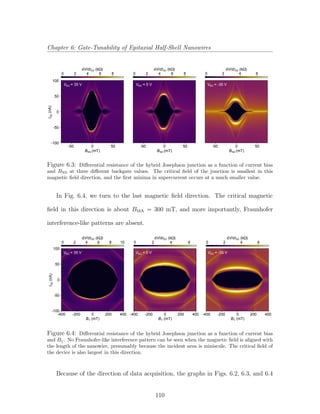
![Chapter 6: Gate-Tunability of Epitaxial Half-Shell Nanowires
are not necessarily symmetric and centered about the origin. Generally, switching
and re-trapping currents in an underdamped Josephson junction do not have the
same magnitude [38]. Sweeping the magnetic field between large values can also be
hysteric. We take horizontal cuts of the graphs in Figs. 6.2 and 6.3 at ISD values
where the critical fields are the largest and plot them in Fig. 6.5.
6
a
b
4
2
0
VBG = 35 V
VBG = 20 V
VBG = 10 V
VBG = 0 V
VBG = -10 V
VBG = -20 V
VBG = -35 V
3
2
1
0
VBG = 35 V
VBG = 30 V
VBG = 25 V
VBG = 20 V
VBG = 0 V
VBG = -8 V
VBG = -14 V
VBG = -20 V
VBG = -25 V
VBG = -30 V
VBG = -35 V
(kSDΩdV/dI)(kSDΩdV/dI)
-200 -100 0 100 200
BNS (mT)
-200 -100 0 100 200
BMinor (mT)
Figure 6.5: Zero-bias (after compensating for hysteresis) differential resistance of the hybrid
Josephson junction as a function of BNS in (a) and as a function of BMinor in (b), at various backgate
voltages. The first minima in the switching current can be identified by a peak in resistance. The
normal state resistance and the magnetic field value at which resistance peak occurs increase with
decreasing backgate voltage.
Similarly, we take vertical cuts of Figs. 6.2 and 6.3 at magnetic field values where
IS and IR are largest and plot them in Fig. 6.6. Panels (a) and (b) of each figure
show cuts from the BNS and BMinor dataset respectively. It is evident from the figures
111](https://image.slidesharecdn.com/4e276476-f8ce-40cc-b3b7-d8e360a550f9-160325143026/85/Chang_gsas-harvard-inactive_0084L_11709-127-320.jpg)
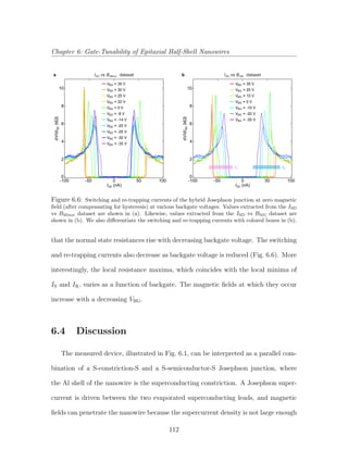
![Chapter 6: Gate-Tunability of Epitaxial Half-Shell Nanowires
for the Meissner effect to manifest. In fact, the thin superconducting leads should
also allow flux penetration, reminiscent of the intermediate laminar state of a Type-I
superconducting slab [38,118].
Treating the device as an extended Josephson junction, the Fraunhofer-like de-
pendence of IS and IR as a function of applied magnetic field can then be attributed
to the interference between supercurrent paths. In rectangular junctions with neg-
ligible magnetic field screening, the interference pattern is a Fraunhofer diffraction
pattern. The local minima of maximal supercurrent occur at integer multiples of the
superconducting flux quanta, Φ0 = h/2e.
45
40
35
30
25
-20-40 0 20 40
90
80
70
60
Area(10-15
m2
)
Area(10-15
m2
)
VBG (V)
Area normal to B
Area normal to B
NS
Minor
Figure 6.7: Assuming that the first zero-bias resistance maxima coincides with one flux quantum
through the Josephson junction, the incident area of the magnetic flux is plotted in this graph. Red
square markers (read against left axis) is the cross-sectional area normal to BNS of the Josephson
junction. Blue circular markers (read against right axis) is the cross-sectional area normal to BMinor.
In the strictest sense, the measured device is not a rectangular extended Josephson
junction. Nonetheless, we can use the Fraunhofer picture to estimate the effective
incident area of magnetic flux. Using the magnetic field value of the local maxima
113](https://image.slidesharecdn.com/4e276476-f8ce-40cc-b3b7-d8e360a550f9-160325143026/85/Chang_gsas-harvard-inactive_0084L_11709-129-320.jpg)
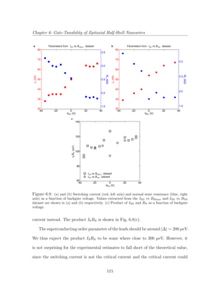
![Chapter 6: Gate-Tunability of Epitaxial Half-Shell Nanowires
in principle be much higher than the measured values. Furthermore, the Josephson
junction is likely diffusive and contacts to the nanowire can be imperfect. Both of
these factors can contribute to a reduced critical current [45]. Even though there is
an unexpected gate-dependence of ISRN, the variation is not large and the product
is largely constant.
6.5 Conclusion
The normal state resistance, the maximum supercurrent, and the effective area
of a segment of half-shell nanowire contacted by two superconducting leads are three
independently measured variables. The backgate-dependence of these three variables
are consistent with one another, and points towards a gate-tunable proximitized semi-
conductor.
116](https://image.slidesharecdn.com/4e276476-f8ce-40cc-b3b7-d8e360a550f9-160325143026/85/Chang_gsas-harvard-inactive_0084L_11709-132-320.jpg)
![Chapter 7: Speculations and Possibilities
7.1 Spin-orbit resolved ABS at finite supercon-
ducting phase difference
Most proposals to induce p-wave superconductivity in nanowires require two cru-
cial ingredients to coexist with proximity effect – (i) few and odd one-dimensional sub-
band occupation (ii) strong spin-orbit coupling. The first criteria has been observed
in a few transport measurements where the maximum supercurrent through a ballis-
tic nanowire Josephson junction was demonstrated to be quantized in steps [34,48].
These observations were attributed to supercurrent carrying ABSs originating from
ballistic one-dimensional conduction channels as described by Beenakker in Ref. [41],
and our discussion in Section 2.5.1. Our experiments discussed in Chapter 5 have
also demonstrated quantized conduction steps in a N-QPC-S device, and on top of
that, showed direct tunneling resonances of the first sub-band ABS. Nonetheless,
it would be reassuring to observe direct tunneling resonances of ABSs from higher
transverse modes of the nanowire, and to investigate their magnetic, spin-orbit, and
superconducting phase dependences.
One of the biggest problems with nanowires is their relatively short mean free
paths. While improvements in materials growth can minimize stacking faults and im-
purities in the crystals, nanofabrication processes will inevitably trash the nanowires.
This is aggravated by the fact that nanowires are relatively naked compared to two-
dimensional electron gas (2DEG) systems which are buried deep within protective
heterostructures.
A solution would be to imitate 2DEG systems and add a non-conductive shell
118](https://image.slidesharecdn.com/4e276476-f8ce-40cc-b3b7-d8e360a550f9-160325143026/85/Chang_gsas-harvard-inactive_0084L_11709-134-320.jpg)
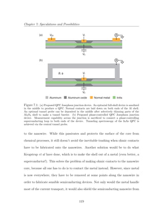
![Chapter 7: Speculations and Possibilities
Figure 7.2: Figure taken from Ref. [119]. The degenerate ABS levels are predicted to split at
finite phase difference across a ballistic Josephson junction with spin-orbit coupling. Here, ε is the
energy of the ABS, ∆ is the pair potential of the superconductor, and φ is the superconducting
phase difference across the Josephson junction.
critical current steps in the superconducting state as the gate voltage is varied. Using
the tunnel probe, one could also measure tunneling resonances associated with each
ABS as the number of transverse modes in the one-dimensional nanowire is increased.
Since the Al shell can be made arbitrarily thin, one could apply a magnetic field along
the length of the nanowire and watch the ABSs spin-split.
Another option is to make a device illustrated in Fig. 7.1(b). We short out both
ends of the Josephson junction with a superconducting loop. While supercurrent
transport measurement is no longer possible, this configuration gives us controllability
over the superconducting phase difference. Using the tunneling probe, one could still
measure the tunneling resonances of ballistic ABSs. At finite superconducting phase
across the Josephson junction, one could observe the splitting of the degenerate ABSs
due to spin-orbit coupling [119]. This experimental signal is illustrated in the graph
taken from Ref. [119] (Fig. 7.2).
121](https://image.slidesharecdn.com/4e276476-f8ce-40cc-b3b7-d8e360a550f9-160325143026/85/Chang_gsas-harvard-inactive_0084L_11709-137-320.jpg)
![Chapter 7: Speculations and Possibilities
In short, selective anodization of Al gives the experimentalist gate-tunability in
the core, passivation of the core, and tunneling spectroscopy capabilities without ever
exposing the InAs core to process chemicals.
7.2 Improved N-QPC-S devices
VG
A
VSD
Figure 7.3: Largely similar to the device in Fig. 7.1(a), except that the tunnel probe is not
necessary and one of the S electrodes is turned into N by evaporating a thick layer or normal metal.
Inverse proximity effect should weaken the Al shell and remove its superconductivity.
One could potentially improve the N-QPC-S device discussed in Chapter 5. Using
the device in Fig. 7.1(a) as a base template, we can do without the middle tunnel
probe and evaporate a thick stack of normal metal on one of the contacts to produce
a final device shown in Fig. 7.3. The idea is to ‘inverse’ proximitize one end of the Al
shell with a large piece of normal metal so that it loses its superconducting properties
(as long as the Al shell is reasonably thin). Assuming that the anodization protects
the InAs core and creates a ballistic junction, we now have a N-QPC-S junction to
execute the proposal by Wimmer et al in Ref. [120].
122](https://image.slidesharecdn.com/4e276476-f8ce-40cc-b3b7-d8e360a550f9-160325143026/85/Chang_gsas-harvard-inactive_0084L_11709-138-320.jpg)
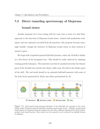
![Chapter 7: Speculations and Possibilities
Once again, we can selectively thin parts of the Al2O3 shell and drop normal metal
electrodes to act as tunnel probes. Multiple probes can be laid down along the length
of the wire to measure the local density of states, as illustrated in Fig. 7.4. Any of
the probes can be activated with at least one other acting as a drain electrode. In
addition, multiple gate electrodes can be fabricated close to the nanowire to provide
gate control over the local carrier density. If Majorana bound states do exist in these
systems, they should show up as sub-gap resonances. Therefore it is of no concern
that the tunnel probes will also probe the density of states of the Al half-shell.
7.4 Little-Parks experiment and the proximity ef-
fect
The Little-Parks experiment demonstrated that the critical temperature of a thin
superconducting cylinder is reduced when the superfluid velocity of Cooper pairs is
increased by threading the cylinder with a magnetic field [121,122]. Because the tran-
sition of resistance as a function of temperature has a finite width near Tc, resistance
of the cylinder was used as a measure of the reduction in critical temperature. As
a result, the resistance of the cylindrical superconductor oscillates with a period of
Φ0 = h/2e and peaks at Φ0/2 mod (Φ0).
In the case of epitaxial full-shell InAs nanowires, one could ask the question:
what happens to proximity effect in the InAs core when magnetic flux is threaded
through the superconducting shell? Using the device schematic in Fig. 7.1(a) as a base
template, we could add additional tunnel probes to the Al shell. We can then measure
124](https://image.slidesharecdn.com/4e276476-f8ce-40cc-b3b7-d8e360a550f9-160325143026/85/Chang_gsas-harvard-inactive_0084L_11709-140-320.jpg)
![Chapter 7: Speculations and Possibilities
the resistance of the device, the tunneling spectrum of the shell, and the tunneling
spectrum of the InAs core as a function of magnetic flux through the quasi-cylindrical
superconducting shell. This would be a nice textbook experiment.
7.5 Class D symmetry in InAs nanowires
While we’re on the topic of phase-controlled experiments, we can also investigate
the mesoscopic symmetry classes of proximitized InAs nanowires. The device in
Fig. 7.1(b) could be used to execute proposals by Altland and Zirnbauer in Refs. [123,
124], although one would have to intentionally trash the InAs junction or make it
longer so that transport through the nanowire is in the diffusive regime (assuming
that the wires are ballistic in the first place).
The proposals also require half a flux quanta to be threaded through the supercon-
ducting loop in order to suppress the induced minigap while retaining the electron-hole
symmetry of a superconductor. In principle, the original phase-controlled devices de-
scribed in Chapters 2 and 3 could have been used for this experiment, but we did
not have access to a vector magnet and the critical field (perpendicular to substrate)
of the device was too low to produce any significant Zeeman energy. With the new
epitaxial full-shell wires, the thin Al shells have exhibited parallel critical fields of
up to 2 T [35]. A vector magnet can thread magnetic flux through the evaporated
superconducting loop while a parallel magnetic field is applied to drive the symmetry
class of the InAs nanowire from DIII to D.
However, if this magnetic field direction were to be chosen for inducing Zeeman
physics, one might have to modify the device in Fig. 7.1(b) by using an epitaxial half-
125](https://image.slidesharecdn.com/4e276476-f8ce-40cc-b3b7-d8e360a550f9-160325143026/85/Chang_gsas-harvard-inactive_0084L_11709-141-320.jpg)
![Appendix A: Device Fabrication
A.1 Making Pre-Fabricated Blanks
Wafer choice
I’ve used degenerately doped Si wafers with a 100 nm thermal oxide for most of
the nanowire experiments. These wafers, purchased from University Wafers, have the
following specifications:
Size: 4”
Crystal axis: [100]
Dopants: Degenerately doped, P-type, Boron
Resistivity: 0.001 - 0.005 Ωcm
Thickness: 500 µm
Thermal Oxide: 100 nm
The thin thermal oxide gives me good capacitive coupling to the nanowires, and
between the backgate and the device, I’ve applied a maximum potential difference
of about 43 V without breaking down the oxide. However, these 100 nm thermal
oxides can leak quite easily, either from intrinsic defects in the substrate, scratches
to the oxide during fabrication, or punctures during wire-bonding. Future fabricators
of nanowire devices might want to consider degenerately doped Si substrates with
thicker thermal oxides, like 200 or 300 nm.
Cleaving the wafer
The idea is to make a lot of pre-fabricated blanks in one go. The photomasks
can make a 6 by 12 grid of chips, and each chip is a 5 mm by 5 mm square. So
128](https://image.slidesharecdn.com/4e276476-f8ce-40cc-b3b7-d8e360a550f9-160325143026/85/Chang_gsas-harvard-inactive_0084L_11709-144-320.jpg)
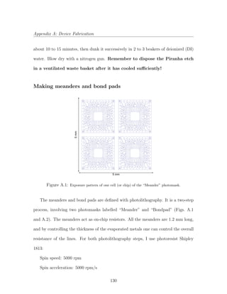
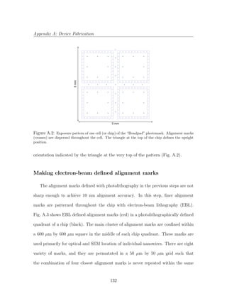
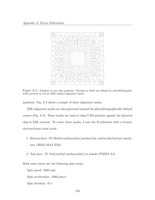
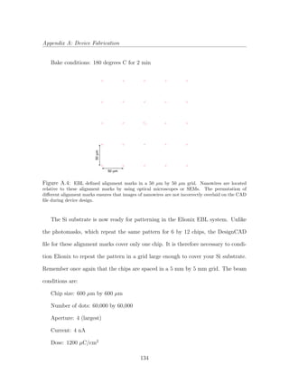
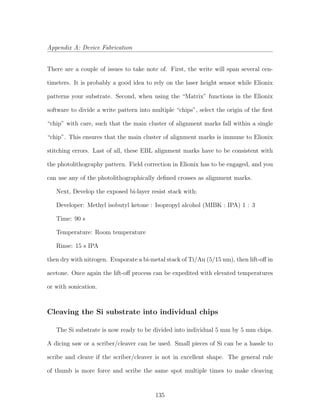
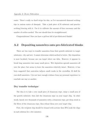

![Appendix A: Device Fabrication
For plasma ashing, using the asher in the QDev cleanroom, I subject my sample
to a 30 s clean.
A.8 Making ohmic contacts to InAs
Stripping native InAs oxide can be achieved chemically or physically. The advan-
tage of a chemical etchant like ammonium polysulfide is that the sulfur content in
the etchant passivates the surface of the InAs nanowire, allowing the device to age
less quickly [33]. The advantage of Ar ion milling is that the Kaufman ion source is
attached to the same vacuum chamber as the electron-beam evaporator, allowing one
to mill and evaporate without exposing the nanowire to ambient conditions.
Regardless of the method used, either process in this section should give you a
near 100% yield.
Chemical etching of native oxide
This recipe originates from Ref. [33]. I pre-mix and store a half-liter batch of
ammonium polysulfide etchant. This generally lasts for about 2 months. To make a
half liter batch, I use:
1. 450 ml of DI water
2. 50 ml of stock ammonium sulfide, 20-24% aqueous solution from VWR Inter-
national
3. 2.4 g of elemental sulfur (powder form)
145](https://image.slidesharecdn.com/4e276476-f8ce-40cc-b3b7-d8e360a550f9-160325143026/85/Chang_gsas-harvard-inactive_0084L_11709-161-320.jpg)
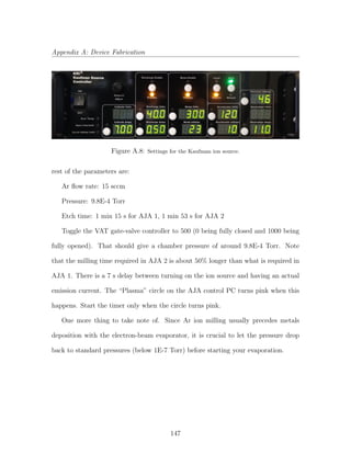
![Appendix A: Device Fabrication
A.9 Making tunnel contacts
Tunnel contacts for devices in Chapters 2, 3 and Ref. [59] are essentially very bad
ohmic contacts. A part of the native InAs oxide is intentionally left behind with
an incomplete etch. This remnant oxide acts as a tunnel barrier. Because it is an
incomplete chemical etch, the final tunneling resistance at room temperature can be
anywhere between 25 kΩ to 10 MΩ.
NOTE: Because the aim is to perform an incomplete etch, contrary to regular
practice, I do not UV Ozone clean or plasma ash the developed sample. I also do not
run to the evaporator to load the sample in a hurry. Instead, I would saunter towards
the evaporator at a leisurely pace after the sample has been etched.
To etch, I use a 7 : 1 buffered oxide etch (BOE). Etch the sample at room
temperature for 7 s, then quench and rinse the in DI water. Blow dry with nitrogen.
Remember to use acid-resistant tweezers!
An alternative to BOE is to use the same ammonium polysulfide etch recipe for
ohmic contacts. However, since we desire an incomplete etch, I etch for 12 min instead
of 17 min. This gives similar tunnel contacts as BOE would.
A.10 Chemical etching of Al shell
Credit goes to Nino Leander Bartolo Ziino for developing this recipe. Aluminum
Etchant Type D manufactured by Transene Company Inc. is the etchant of choice.
Warm it up to 55 degrees C in a closed beaker with a hot water bath. The etch is
only 10 s, so get the timing right! The etchant eats bare Al very rapidly. Most of the
148](https://image.slidesharecdn.com/4e276476-f8ce-40cc-b3b7-d8e360a550f9-160325143026/85/Chang_gsas-harvard-inactive_0084L_11709-164-320.jpg)
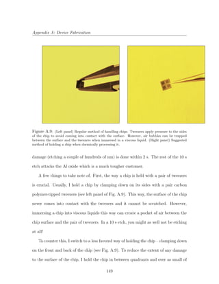
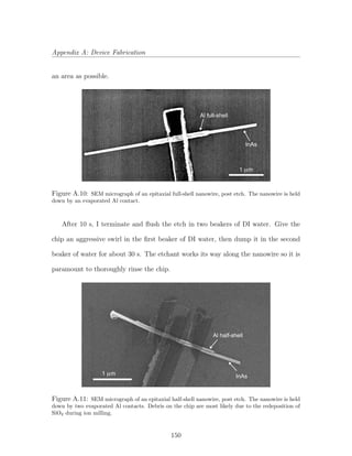
![Appendix B: Electrical Filtering
More care could be taken to shield the sample space [125].
B.1 Overall layout
I’ve set up two different fridges and measured in three, so the filter setup has been
changed multiple times. However, the components in each fridge are similar, and the
general principle is identical. This section describes the general layout of Marcus 3,
Triton 1, and Triton 3 dilution fridges.
B.1.1 Marcus 3
Marcus 3 is the third cryo-free dilution refrigerator in old Marcus lab (we’re not
tremendously creative when it comes to naming things). I very much prefer Marcus 3
because it was configured purely for DC measurements and it had a very nice feature
– a shielded coldfinger. The coldfinger and sample puck assembly was designed by
Angela Kou [126]. The detached coldfinger, shown in Fig. B.1, is machined from a
single piece of copper and then gold-plated.
A bore runs along the length of the otherwise solid coldfinger. This allows any
wiring threaded through the bore to be completely shielded between the mixing cham-
ber plate and the device. We extended this column by adding a copper box to the
top of the coldfinger. The copper box houses a copper powder filter and a sapphire
box.
The copper powder filter serves as a block to high frequency radiation through
skin-effect damping between the insulated wires and the surrounding copper powder.
The sapphire box thermalizes the electrons with the mixing chamber plate through
153](https://image.slidesharecdn.com/4e276476-f8ce-40cc-b3b7-d8e360a550f9-160325143026/85/Chang_gsas-harvard-inactive_0084L_11709-169-320.jpg)
![Appendix B: Electrical Filtering
Copper
Powder
Sapphire
Box
to sample
MCplateShielded
Coldfinger
to breakout box
to sample
RF
RC
Cu powder
Sapphire
Sapphire
Figure B.1: Filter setup on Marcus 3. Left panel shows a picture of the shielded coldfinger
arrangement. Components in the shielded coldfinger are illustrated in the center panel. Right panel
shows the overall layout of the filter arrangement.
dissipative meanders fabricated on sapphire plates – an electrically insulating material
known for good thermal conductivity at low temperatures [127].
The rest of the filters are mounted on the mixing chamber plate, as illustrated in
the rightmost panel of Fig. B.1. The RF filter is a series of LC low-pass filters with
cutoff frequencies beginning at 80 MHz. The RC filter has a single 80 MHz-cutoff
LC filter and two RC low-pass filters. Finally, another sapphire box is also mounted
directly to the mixing chamber plate to provide additional thermalization.
At various stages of the fridge we mount copper thermalization posts for additional
thermalization. These are cylinders made out of high-conductivity copper. Looms
comprising of twelve twisted pairs of constanstan wires wrap around the copper cylin-
der. The same type of loom connects the various stages of filtering together.
The result of the addition of the custom coldfinger and various filtering/thermalization
154](https://image.slidesharecdn.com/4e276476-f8ce-40cc-b3b7-d8e360a550f9-160325143026/85/Chang_gsas-harvard-inactive_0084L_11709-170-320.jpg)
![Appendix B: Electrical Filtering
8 mK
5/2 7/38/3
12 mK
24 mK
36 mK
56 mK
150 mK
Figure B.2: Figure taken from Ref. [128]. Longitudinal resistance of a GaAs 2-DEG hall-bar in the
fractional quantum hall regime is measured as a function of magnetic field at various temperatures.
1500
1000
5/2 7/38/3
500
0
Rxx(Ohms)
500045004000
B (mT)
Original setup
Addition of filters and new coldfinger
Figure B.3: Longitudinal resistance of a hall-bar made from the same GaAs wafer as the device
Jeff Miller measured in Ref. [128]. The hall-bar was measured before (red) and after (blue) the
installation of the custom coldfinger and filtering/thermalization modules.
155](https://image.slidesharecdn.com/4e276476-f8ce-40cc-b3b7-d8e360a550f9-160325143026/85/Chang_gsas-harvard-inactive_0084L_11709-171-320.jpg)
![Appendix B: Electrical Filtering
modules can be seen in Fig. B.3. We measure the longitudinal resistance, Rxx, of a
GaAs 2DEG hall bar (wafer I.D. P2-25-05, grown by L. Pfeiffer and K. West) at
filling factors close to ν = 5/2. Features in longitudinal resistance around ν = 5/2 is
very sensitive to temperature, and can be used as a metric for electron temperature.
Fig. B.2, taken from Ref. [128], shows the temperature dependence of Rxx.
Qualitative comparison between data in Fig. B.3 and data in Fig. B.2 suggests an
electron temperature in excess of 100 mK in the original configuration of the fridge.
After modification, we see a sharp reduction of Rxx at ν = 5/2. However, it does not
reach 0 as it should at temperatures below 20 mK (Fig. B.2). We estimate our final
electron temperature to be somewhere around 30 mK.
With extensive modifications to the coldfinger and sample holder, it is possible
to reach electron temperatures of sub 20 mK in these cryo-free dilution refrigerators
[126]. Fortunately, the superconductivity related experiments carried out in Marcus
3 are relatively insensitive to temperatures below 50 mK.
Electron temperature aside, I would like to note the importance of the RF filter
box and the 80 MHz π7
filter in the RC filter box. Because the initial setup of
the RC filters was too aggressive, we once removed the RC filter box completely.
To our dismay, the transition in the IV curve between the superconducting branch
and the normal state branch of an InAs Josephson junction was smoothened out.
Additionally, the superconducting branch of the IV curve had a finite gradient. The
effects were somewhat offset by applying additional VLFX-80 filters to the breakout
box at room temperature, or by reinstalling the RC filter with just the 80 MHz π7
filter (without R and C components). This suggested to us that high frequency noise
156](https://image.slidesharecdn.com/4e276476-f8ce-40cc-b3b7-d8e360a550f9-160325143026/85/Chang_gsas-harvard-inactive_0084L_11709-172-320.jpg)

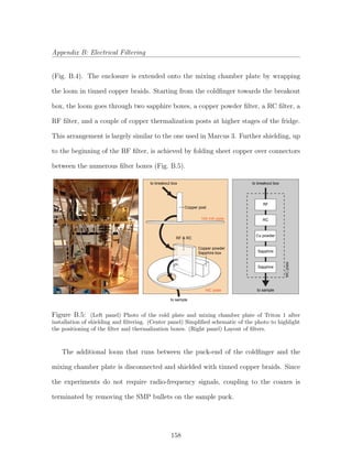
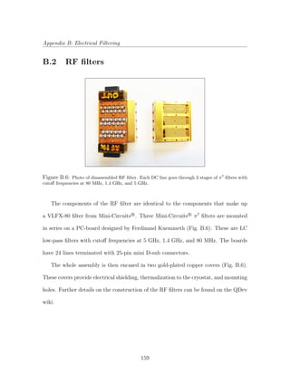
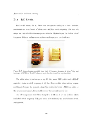
![Appendix B: Electrical Filtering
B.4 Copper powder filters
The idea behind a metal powder filter, reported in Refs. [129–133], is to surround
an insulated wire in close proximity with a large-surface-area conductor. To do so, we
pack coiled and insulated copper wires into a copper enclosure and fill the enclosure
with fine-grain copper powder. The copper powder provides a large surface area and
produces significant skin-effect damping of high frequency signals in the copper wire.
However, such a filter box provides challenges to the vacuum environment of a
dilution refrigerator. Fine grain copper powder in an enclosed space meant that a
lot of air would be trapped. To overcome this problem, we pack the copper powder
and the central wire into an epoxy ‘ravioli’ (or ‘dumpling’, if you wish). The epoxy
enclosed ‘ravioli’ would then prevent the copper powder filter from outgassing into
the vacuum chamber of the fridge.
Unfortunately, I do not have any pictures of a disassembled copper powder filter
box, since the lids are epoxy-ed shut. To assemble one, we coil fine insulated copper
wires with a handheld power drill. The cylindrical surface of the drill bit helps to coil
the wire efficiently and with a constant diameter.
The coiled wires are then soldered on both ends to mini D-sub connectors that
are already mounted on the copper powder enclosure (see QDev wiki for their CAD
drawings). Next, we close the lid of the copper box on one side, and line the bottom
and walls with StycastR
2850 FT epoxy. This epoxy has the added advantage of being
thermally conductive, and so helps in the thermalization of the central wires. Once
the epoxy has set and dried, we fill the ‘half-ravioli’ with copper powder (copper, and
not stainless steel, to prevent stray magnetism). To compactify the copper powder,
161](https://image.slidesharecdn.com/4e276476-f8ce-40cc-b3b7-d8e360a550f9-160325143026/85/Chang_gsas-harvard-inactive_0084L_11709-177-320.jpg)
![Appendix B: Electrical Filtering
we apply a handheld vibrator to the copper enclosure. After sufficient quantities of
copper powder have been packed in, we seal the top of the copper box with more
epoxy, and screw the lid on. Before the epoxy ‘lid’ can set, we place the copper
powder filter box into a vacuum chamber and pump on it with a wet pump. This
removes air pockets trapped between the copper grains and the epoxy.
B.5 Sapphire boxes
Sapphire boxes are highly crucial for electron thermalization below 1 K. The
operating principle is simple: let warm electrons from the measurement circuit come
into contact with a cold surface for an extended period of time. The coldest surface
in the fridge would be the mixing chamber plate. However, since it is electrically
conducting, it would be impossible to directly thermalize more than one measurement
line. To solve this problem, we attach sapphire plates to high-conductivity copper
boxes. Sapphire is an electrical insulator, and an excellent thermal conductor at low
temperatures [127].
A disassembled sapphire box is shown in Fig. B.8. Two sapphire plates are
mounted on opposing sides of the copper box. Each sapphire plate has 12 meanders
to give a total of 24 DC measurement lines. The meanders are made by evaporating
a 30/250 nm Cr/Au film onto the entire surface of the sapphire plate. They are then
defined with photolithography and subsequently etched to remove unwanted metals.
Finally, the sapphire plate with evaporated meanders are then annealed at high tem-
peratures. The recipe can be found in Angela’s thesis, Ref. [126], and also on the
QDev wiki.
162](https://image.slidesharecdn.com/4e276476-f8ce-40cc-b3b7-d8e360a550f9-160325143026/85/Chang_gsas-harvard-inactive_0084L_11709-178-320.jpg)
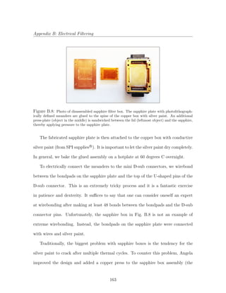
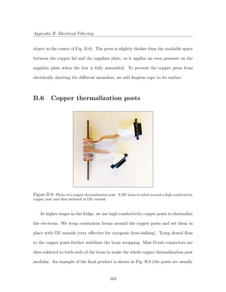
![Bibliography
[1] R. Holm and W. Meissner, Einige kontaktwiderstandsmessungen bei tiefen tem-
peraturen, Z. Phys. 86, 787 (1933).
[2] H. Meissner, Superconductivity of contacts with interposed barriers, Phys. Rev.
117, 672 (1960).
[3] L. Fu and C. L. Kane, Superconducting proximity effect and Majorana fermions
at the surface of a topological insulator, Phys. Rev. Lett. 100, 096407 (2008).
[4] L. Fu and C. L. Kane, Josephson current and noise at a
superconductor/quantum-spin-Hall-insulator/superconductor junction, Phys.
Rev. B 79, 161408 (2009).
[5] A. Cook and M. Franz, Majorana fermions in a topological-insulator nanowire
proximity-coupled to an s-wave superconductor, Phys. Rev. B 84, 201105 (2011).
[6] A. Y. Kitaev, Unpaired Majorana fermions in quantum wires, Phys. Usp. 44,
131 (2001).
[7] R. M. Lutchyn, J. D. Sau, and S. Das Sarma, Majorana fermions and a topo-
logical phase transition in semiconductor-superconductor heterostructures, Phys.
Rev. Lett. 105, 077001 (2010).
[8] Y. Oreg, G. Refael, and F. von Oppen, Helical liquids and Majorana bound
states in quantum wires, Phys. Rev. Lett. 105, 177002 (2010).
[9] J. D. Sau, R. M. Lutchyn, S. Tewari, and S. Das Sarma, Generic new plat-
form for topological quantum computation using semiconductor heterostructures,
Phys. Rev. Lett. 104, 040502 (2010).
[10] J. Alicea, Majorana fermions in a tunable semiconductor device, Phys. Rev. B
81, 125318 (2010).
[11] A. Kitaev, Fault-tolerant quantum computation by anyons, Ann. Phys. 303, 2
(2003).
166](https://image.slidesharecdn.com/4e276476-f8ce-40cc-b3b7-d8e360a550f9-160325143026/85/Chang_gsas-harvard-inactive_0084L_11709-182-320.jpg)
![Bibliography
[12] C. Nayak, S. H. Simon, A. Stern, M. Freedman, and S. Das Sarma, Non-Abelian
anyons and topological quantum computation, Rev. Mod. Phys. 80, 1083 (2008).
[13] J. Alicea, Y. Oreg, G. Refael, F. von Oppen, and M. P. A. Fisher, Non-abelian
statistics and topological quantum information processing in 1D wire networks,
Nat. Phys. 7, 412 (2011).
[14] J. D. Sau, S. Tewari, and S. Das Sarma, Universal quantum computation in a
semiconductor quantum wire network, Phys. Rev. A 82, 052322 (2010).
[15] B. van Heck, A. R. Akhmerov, F. Hassler, M. Burrello, and C. W. J. Beenakker,
Coulomb-assisted braiding of Majorana fermions in a Josephson junction array,
New J. Phys. 14, 035019 (2012).
[16] C. Nayak, S. H. Simon, A. Stern, M. Freedman, and S. Das Sarma, Non-Abelian
anyons and topological quantum computation, Rev. Mod. Phys. 80, 1083 (2008).
[17] F. Wilczek, Majorana returns, Nat. Phys. 5, 614 (2009).
[18] V. Mourik, K. Zuo, S. M. Frolov, S. R. Plissard, E. P. A. M. Bakkers, and
L. P. Kouwenhoven, Signatures of Majorana fermions in hybrid superconductor-
semiconductor nanowire devices, Science 336, 1003 (2012).
[19] A. Das, Y. Ronen, Y. Most, Y. Oreg, M. Heiblum, and H. Shtrikman, Zero-
bias peaks and splitting in an Al-InAs nanowire topological superconductor as a
signature of Majorana fermions, Nat. Phys. 8, 887 (2012).
[20] M. T. Deng, C. L. Yu, G. Y. Huang, M. Larsson, P. Caroff, and H. Q. Xu,
Anomalous zero-bias conductance peak in a Nb-InSb nanowire-Nb hybrid device,
Nano Lett. 12, 6414 (2012).
[21] A. D. K. Finck, D. J. Van Harlingen, P. K. Mohseni, K. Jung, and X. Li,
Anomalous modulation of a zero-bias peak in a hybrid nanowire-superconductor
device, Phys. Rev. Lett. 110, 126406 (2013).
[22] H. O. H. Churchill, V. Fatemi, K. Grove-Rasmussen, M. T. Deng, P. Caroff,
H. Q. Xu, and C. M. Marcus, Superconductor-nanowire devices from tunnel-
ing to the multichannel regime: Zero-bias oscillations and magnetoconductance
crossover, Phys. Rev. B 87, 241401 (2013).
[23] M. T. Bj¨ork, A. Fuhrer, A. E. Hansen, M. W. Larsson, L. E. Fr¨oberg, and
L. Samuelson, Tunable effective g factor in InAs nanowire quantum dots, Phys.
Rev. B 72, 201307 (2005).
[24] Y. A. Bychkov and E. I. Rashba, Oscillatory effects and the magnetic suscepti-
bility of carriers in inversion layers, J. Phys. C Solid State 17, 6039 (1984).
167](https://image.slidesharecdn.com/4e276476-f8ce-40cc-b3b7-d8e360a550f9-160325143026/85/Chang_gsas-harvard-inactive_0084L_11709-183-320.jpg)
![Bibliography
[25] S. Est´evez Hern´andez, M. Akabori, K. Sladek, C. Volk, S. Alagha, H. Hardt-
degen, M. G. Pala, N. Demarina, D. Gr¨utzmacher, and T. Sch¨apers, Spin-orbit
coupling and phase coherence in InAs nanowires, Phys. Rev. B 82, 235303
(2010).
[26] D. Liang and X. P. Gao, Strong tuning of Rashba spinorbit interaction in single
InAs nanowires, Nano Lett. 12, 3263 (2012).
[27] A. E. Hansen, M. T. Bj¨ork, C. Fasth, C. Thelander, and L. Samuelson, Spin
relaxation in InAs nanowires studied by tunable weak antilocalization, Phys.
Rev. B 71, 205328 (2005).
[28] C. Fasth, A. Fuhrer, L. Samuelson, V. N. Golovach, and D. Loss, Direct mea-
surement of the spin-orbit interaction in a two-electron InAs nanowire quantum
dot, Phys. Rev. Lett. 98, 266801 (2007).
[29] S. Nadj-Perge, S. M. Frolov, E. P. A. M. Bakkers, and L. P. Kouwenhoven,
Spin-orbit qubit in a semiconductor nanowire, Nature 468 (2010).
[30] Y.-J. Doh, J. A. van Dam, A. L. Roest, E. P. A. M. Bakkers, L. P. Kouwenhoven,
and S. De Franceschi, Tunable supercurrent through semiconductor nanowires,
Science 309, 272 (2005).
[31] L. O. Olsson, C. B. M. Andersson, M. C. H˚akansson, J. Kanski, L. Ilver, and
U. O. Karlsson, Charge accumulation at InAs surfaces, Phys. Rev. Lett. 76,
3626 (1996).
[32] C. A. Mead and W. G. Spitzer, Fermi level position at semiconductor surfaces,
Phys. Rev. Lett. 10, 471 (1963).
[33] D. B. Suyatin, C. Thelander, M. T. Bj¨ork, I. Maximov, and L. Samuelson, Sulfur
passivation for ohmic contact formation to InAs nanowires, Nanotechnology 18,
105307 (2007).
[34] S. Abay, D. Persson, H. Nilsson, H. Q. Xu, M. Fogelstrm, V. Shumeiko, and
P. Delsing, Quantized conductance and its correlation to the supercurrent in a
nanowire connected to superconductors, Nano Lett. 13, 3614 (2013).
[35] N. L. B. Ziino, P. Krogstrup, M. H. Madsen, E. Johnson, J. B. Wagner, C. M.
Marcus, J. Nyg˚ard, and T. S. Jespersen, Epitaxial aluminum contacts to InAs
nanowires, ArXiv e-prints (2013).
[36] E. J. H. Lee, X. Jiang, M. Houzet, R. Aguado, C. M. Lieber, and
S. De Franceschi, Spin-resolved Andreev levels and parity crossings in hybrid
superconductor-semiconductor nanostructures, Nat. Nanotechnol. 9, 79 (2014).
168](https://image.slidesharecdn.com/4e276476-f8ce-40cc-b3b7-d8e360a550f9-160325143026/85/Chang_gsas-harvard-inactive_0084L_11709-184-320.jpg)
![Bibliography
[37] R. M. Lutchyn, T. D. Stanescu, and S. Das Sarma, Search for Majorana
fermions in multiband semiconducting nanowires, Phys. Rev. Lett. 106, 127001
(2011).
[38] M. Tinkham, Introduction to Superconductivity: Second Edition, Dover Books
on Physics (Dover Publications, 2004).
[39] T. Klapwijk, Proximity effect from an Andreev perspective, J. Supercond. 17,
593 (2004).
[40] B. Pannetier and H. Courtois, Andreev reflection and proximity effect, J. Low
Temp. Phys. 118, 599 (2000).
[41] C. Beenakker, Three “universal” mesoscopic Josephson effects, in Transport
Phenomena in Mesoscopic Systems, edited by H. Fukuyama and T. Ando,
Springer Series in Solid-State Sciences, Vol. 109, 235–253 (Springer Berlin Hei-
delberg, 1992).
[42] C. Beenakker and H. van Houten, The superconducting quantum point contact,
in Nanostructures and Mesoscopic Systems, edited by W. P. Kirk and M. A.
Reed, 481 – 497 (Academic Press, 1992).
[43] L. Bretheau, Localized excitations in superconducting atomic contacts: Probing
the Andreev doublet, Ph.D. thesis, CEA-Saclay (2013).
[44] G. E. Blonder, M. Tinkham, and T. M. Klapwijk, Transition from metallic to
tunneling regimes in superconducting microconstrictions: Excess current, charge
imbalance, and supercurrent conversion, Phys. Rev. B 25, 4515 (1982).
[45] J. C. Hammer, J. C. Cuevas, F. S. Bergeret, and W. Belzig, Density of states
and supercurrent in diffusive SNS junctions: Roles of nonideal interfaces and
spin-flip scattering, Phys. Rev. B 76, 064514 (2007).
[46] T. Klapwijk, G. Blonder, and M. Tinkham, Explanation of subharmonic energy
gap structure in superconducting contacts, Physica B & C 109 110, Part 3,
1657 (1982), 16th International Conference on Low Temperature Physics.
[47] E. N. Bratus’, V. S. Shumeiko, and G. Wendin, Theory of subharmonic gap
structure in superconducting mesoscopic tunnel contacts, Phys. Rev. Lett. 74,
2110 (1995).
[48] J. Xiang, A. Vidan, M. Tinkham, R. M. Westervelt, and C. M. Lieber, Ge/Si
nanowire mesoscopic Josephson junctions, Nat. Nanotechnol. 1, 208 (2006).
[49] G. Eilenberger, Transformation of Gorkov’s equation for type II superconductors
into transport-like equations, Z. Phys. 214, 195 (1968).
169](https://image.slidesharecdn.com/4e276476-f8ce-40cc-b3b7-d8e360a550f9-160325143026/85/Chang_gsas-harvard-inactive_0084L_11709-185-320.jpg)
![Bibliography
[50] K. D. Usadel, Generalized diffusion equation for superconducting alloys, Phys.
Rev. Lett. 25, 507 (1970).
[51] W. L. McMillan, Tunneling model of the superconducting proximity effect, Phys.
Rev. 175, 537 (1968).
[52] A. A. Golubov and M. Y. Kupriyanov, Josephson effect in SNlNS and SNIS
tunnel structures with finite transparency of the sn boundaries, Zh. ´Eksp. Teor.
Fiz. 96, 1420 (1989).
[53] W. Belzig, C. Bruder, and G. Sch¨on, Local density of states in a dirty normal
metal connected to a superconductor, Phys. Rev. B 54, 9443 (1996).
[54] W. Belzig, F. K. Wilhelm, C. Bruder, G. Sch¨on, and A. D. Zaikin, Quasiclassical
green’s function approach to mesoscopic superconductivity, Superlattice Microst.
25, 1251 (1999).
[55] D. A. Ivanov, R. von Roten, and G. Blatter, Minigap in a long disordered SNS
junction: Analytical results, Phys. Rev. B 66, 052507 (2002).
[56] S. Gu´eron, H. Pothier, N. O. Birge, D. Esteve, and M. H. Devoret, Supercon-
ducting proximity effect probed on a mesoscopic length scale, Phys. Rev. Lett.
77, 3025 (1996).
[57] N. Moussy, H. Courtois, and B. Pannetier, Local spectroscopy of a proximity
superconductor at very low temperature, Europhys. Lett. 55, 861 (2001).
[58] L. Serrier-Garcia, J. C. Cuevas, T. Cren, C. Brun, V. Cherkez, F. Debontridder,
D. Fokin, F. S. Bergeret, and D. Roditchev, Scanning tunneling spectroscopy
study of the proximity effect in a disordered two-dimensional metal, Phys. Rev.
Lett. 110, 157003 (2013).
[59] W. Chang, V. E. Manucharyan, T. S. Jespersen, J. Nyg˚ard, and C. M. Mar-
cus, Tunneling spectroscopy of quasiparticle bound states in a spinful Josephson
junction, Phys. Rev. Lett. 110, 217005 (2013).
[60] F. Zhou and B. Spivak, Resistance of superconductor-normal-metal-
superconductor (SNS) junctions, J. Exp. Theor. Phys. Lett. 65, 369 (1997).
[61] H. le Sueur, P. Joyez, H. Pothier, C. Urbina, and D. Esteve, Phase controlled
superconducting proximity effect probed by tunneling spectroscopy, Phys. Rev.
Lett. 100, 197002 (2008).
[62] J. Reutlinger, L. Glazman, Y. V. Nazarov, and W. Belzig, “Smile” gap in the
density of states of a cavity between superconductors, Phys. Rev. Lett. 112,
067001 (2014).
170](https://image.slidesharecdn.com/4e276476-f8ce-40cc-b3b7-d8e360a550f9-160325143026/85/Chang_gsas-harvard-inactive_0084L_11709-186-320.jpg)
![Bibliography
[63] A. Levchenko, Crossover in the local density of states of mesoscopic
superconductor/normal-metal/superconductor junctions, Phys. Rev. B 77,
180503 (2008).
[64] E. Vecino, A. Mart´ın-Rodero, and A. L. Yeyati, Josephson current through a
correlated quantum level: Andreev states and π junction behavior, Phys. Rev.
B 68, 035105 (2003).
[65] T. Doma´nski and A. Donabidowicz, Interplay between particle-hole splitting and
the Kondo effect in quantum dots, Phys. Rev. B 78, 073105 (2008).
[66] T. Meng, S. Florens, and P. Simon, Self-consistent description of Andreev bound
states in Josephson quantum dot devices, Phys. Rev. B 79, 224521 (2009).
[67] A. Mart´ın-Rodero and A. Levy Yeyati, Josephson and Andreev transport through
quantum dots, Adv. Phys. 60, 899 (2011).
[68] M. Grobis, I. G. Rau, R. M. Potok, and D. Goldhaber-Gordon, Kondo effect in
mesoscopic quantum dots, eprint arXiv:cond-mat/0611480 (2006).
[69] L. Yu, Bound state in superconductors with paramagnetic impurities, Acta Phys.
Sin. 21, 75 (1965).
[70] H. Shiba, Classical spins in superconductors, Prog. Theor. Phys. 40, 435 (1968).
[71] A. I. Rusinov, Theory of gapless superconductivity in alloys containing param-
agnetic impurities, Sov. Phys., JETP 29, 1101 (1969).
[72] S. de Franceschi, L. Kouwenhoven, C. Schonenberger, and W. Wernsdorfer,
Hybrid superconductor-quantum dot devices, Nat. Nanotechnol. 5, 703 (2010).
[73] D. Goldhaber-Gordon, H. Shtrikman, D. Mahalu, D. Abusch-Magder,
U. Meirav, and M. A. Kastner, Kondo effect in a single-electron transistor,
Nature 391, 156 (1998).
[74] A. V. Balatsky, I. Vekhter, and J.-X. Zhu, Impurity-induced states in conven-
tional and unconventional superconductors, Rev. Mod. Phys. 78, 373 (2006).
[75] T. Soda, T. Matsuura, and Y. Nagaoka, s-d Exchange interaction in a super-
conductor, Prog. Theor. Phys. 38, 551 (1967).
[76] H. Shiba and T. Soda, Superconducting tunneling through the barrier with para-
magnetic impurities, Prog. Theor. Phys. 41, 25 (1969).
[77] K. Satori, H. Shiba, O. Sakai, and Y. Shimizu, Numerical renormalization group
study of magnetic impurities in superconductors, J. Phys. Soc. Jpn 61, 3239
(1992).
171](https://image.slidesharecdn.com/4e276476-f8ce-40cc-b3b7-d8e360a550f9-160325143026/85/Chang_gsas-harvard-inactive_0084L_11709-187-320.jpg)
![Bibliography
[78] J. Simonin and R. Allub, Rare-earth impurity in a superconductive matrix, Phys.
Rev. Lett. 74, 466 (1995).
[79] J. Bauer, A. Oguri, and A. C. Hewson, Spectral properties of locally correlated
electrons in a Bardeen Cooper Schrieffer superconductor, J. Phys-Condens. Mat.
19, 486211 (2007).
[80] K. J. Franke, G. Schulze, and J. I. Pascual, Competition of superconducting
phenomena and Kondo screening at the nanoscale, Science 332, 940 (2011).
[81] M. R. Buitelaar, T. Nussbaumer, and C. Sch¨onenberger, Quantum dot in the
Kondo regime coupled to superconductors, Phys. Rev. Lett. 89, 256801 (2002).
[82] L. I. Glazman and K. A. Matveev, Resonant Josephson current through Kondo
impurities in a tunnel barrier, JETP Lett. 49, 659 (1989).
[83] B. I. Spivak and S. A. Kivelson, Negative local superfluid densities: The dif-
ference between dirty superconductors and dirty Bose liquids, Phys. Rev. B 43,
3740 (1991).
[84] A. V. Rozhkov, D. P. Arovas, and F. Guinea, Josephson coupling through a
quantum dot, Phys. Rev. B 64, 233301 (2001).
[85] A. V. Rozhkov and D. P. Arovas, Interacting-impurity Josephson junction:
Variational wave functions and slave-boson mean-field theory, Phys. Rev. B
62, 6687 (2000).
[86] Y. Tanaka, A. Oguri, and A. C. Hewson, Kondo effect in asymmetric Josephson
couplings through a quantum dot, New J. Phys. 9, 115 (2007).
[87] J. A. van Dam, Y. V. Nazarov, E. P. A. M. Bakkers, S. De Franceschi, and L. P.
Kouwenhoven, Supercurrent reversal in quantum dots, Nature 442, 667 (2006).
[88] J. P. Cleuziou, W. Wernsdorfer, V. Bouchiat, T. Ondar¸cuhu, and M. Monthioux,
Carbon nanotube superconducting quantum interference device, Nat. Nanotech-
nol. 1, 53 (2006).
[89] H. I. Jørgensen, T. Novotn´y, K. Grove-Rasmussen, K. Flensberg, and P. E.
Lindelof, Critical current 0-π transition in designed Josephson quantum dot
junctions, Nano Lett. 7, 2441 (2007).
[90] A. Eichler, R. Deblock, M. Weiss, C. Karrasch, V. Meden, C. Sch¨onenberger,
and H. Bouchiat, Tuning the Josephson current in carbon nanotubes with the
Kondo effect, Phys. Rev. B 79, 161407 (2009).
172](https://image.slidesharecdn.com/4e276476-f8ce-40cc-b3b7-d8e360a550f9-160325143026/85/Chang_gsas-harvard-inactive_0084L_11709-188-320.jpg)
![Bibliography
[91] R. Maurand, T. Meng, E. Bonet, S. Florens, L. Marty, and W. Wernsdorfer,
First-order 0-π quantum phase transition in the Kondo regime of a supercon-
ducting carbon-nanotube quantum dot, Phys. Rev. X 2, 011009 (2012).
[92] D. J. Luitz, F. F. Assaad, T. Novotn´y, C. Karrasch, and V. Meden, Under-
standing the Josephson current through a Kondo-correlated quantum dot, Phys.
Rev. Lett. 108, 227001 (2012).
[93] T. Dirks, T. L. Hughes, S. Lal, B. Uchoa, Y.-F. Chen, C. Chialvo, P. M. Gold-
bart, and N. Mason, Transport through Andreev bound states in a graphene
quantum dot, Nat. Phys. 7, 386 (2011).
[94] R. S. Deacon, Y. Tanaka, A. Oiwa, R. Sakano, K. Yoshida, K. Shibata, K. Hi-
rakawa, and S. Tarucha, Tunneling spectroscopy of Andreev energy levels in a
quantum dot coupled to a superconductor, Phys. Rev. Lett. 104, 076805 (2010).
[95] R. S. Deacon, Y. Tanaka, A. Oiwa, R. Sakano, K. Yoshida, K. Shibata, K. Hi-
rakawa, and S. Tarucha, Kondo-enhanced Andreev transport in single self-
assembled InAs quantum dots contacted with normal and superconducting leads,
Phys. Rev. B 81, 121308 (2010).
[96] E. J. H. Lee, X. Jiang, R. Aguado, G. Katsaros, C. M. Lieber, and
S. De Franceschi, Zero-bias anomaly in a nanowire quantum dot coupled to
superconductors, Phys. Rev. Lett. 109, 186802 (2012).
[97] J.-D. Pillet, C. H. L. Quay, P. Morfin, C. Bena, A. L. Yeyati, and P. Joyez,
Andreev bound states in supercurrent-carrying carbon nanotubes revealed, Nat.
Phys. 6, 965 (2010).
[98] T. S. Jespersen, M. Aagesen, C. Sørensen, P. E. Lindelof, and J. Nyg˚ard, Kondo
physics in tunable semiconductor nanowire quantum dots, Phys. Rev. B 74,
233304 (2006).
[99] A. V. Kretinin, H. Shtrikman, D. Goldhaber-Gordon, M. Hanl, A. Weichsel-
baum, J. von Delft, T. Costi, and D. Mahalu, Spin-1/2 Kondo effect in an
InAs nanowire quantum dot: Unitary limit, conductance scaling, and Zeeman
splitting, Phys. Rev. B 84, 245316 (2011).
[100] C. H. L. Quay, J. Cumings, S. J. Gamble, R. d. Picciotto, H. Kataura, and
D. Goldhaber-Gordon, Magnetic field dependence of the spin-1/2 and spin-1
Kondo effects in a quantum dot, Phys. Rev. B 76, 245311 (2007).
[101] V. Koerting, B. M. Andersen, K. Flensberg, and J. Paaske, Nonequilibrium
transport via spin-induced subgap states in superconductor/quantum dot/normal
metal cotunnel junctions, Phys. Rev. B 82, 245108 (2010).
173](https://image.slidesharecdn.com/4e276476-f8ce-40cc-b3b7-d8e360a550f9-160325143026/85/Chang_gsas-harvard-inactive_0084L_11709-189-320.jpg)
![Bibliography
[102] A. V. Rozhkov and D. P. Arovas, Josephson coupling through a magnetic im-
purity, Phys. Rev. Lett. 82, 2788 (1999).
[103] A. Oguri, Y. Tanaka, and J. Bauer, Interplay between Kondo and Andreev-
Josephson effects in a quantum dot coupled to one normal and two supercon-
ducting leads, Phys. Rev. B 87, 075432 (2013).
[104] D. Goldhaber-Gordon, J. G¨ores, M. A. Kastner, H. Shtrikman, D. Mahalu, and
U. Meirav, From the Kondo regime to the mixed-valence regime in a single-
electron transistor, Phys. Rev. Lett. 81, 5225 (1998).
[105] S. Takei, B. M. Fregoso, H.-Y. Hui, A. M. Lobos, and S. Das Sarma, Soft
superconducting gap in semiconductor Majorana nanowires, Phys. Rev. Lett.
110, 186803 (2013).
[106] T. D. Stanescu, R. M. Lutchyn, and S. Das Sarma, Soft superconducting gap in
semiconductor-based Majorana nanowires, ArXiv e-prints (2013).
[107] D. Rainis and D. Loss, Majorana qubit decoherence by quasiparticle poisoning,
Phys. Rev. B 85, 174533 (2012).
[108] M. Cheng, R. M. Lutchyn, and S. Das Sarma, Topological protection of Majo-
rana qubits, Phys. Rev. B 85, 165124 (2012).
[109] P. Krogstrup, J. Yamasaki, C. B. Sørensen, E. Johnson, J. B. Wagner, R. Pen-
nington, M. Aagesen, N. Tanaka, and J. Nygrd, Junctions in axial III-V het-
erostructure nanowires obtained via an interchange of group III elements, Nano
Lett. 9, 3689 (2009), pMID: 19842690.
[110] C. W. J. Beenakker, Quantum transport in semiconductor-superconductor mi-
crojunctions, Phys. Rev. B 46, 12841 (1992).
[111] A. F. Andreev, Thermal conductivity of the intermediate state of superconduc-
tors, Soviet Phys., JETP 46, 1823 (1964).
[112] S. Chuang, Q. Gao, R. Kapadia, A. C. Ford, J. Guo, and A. Javey, Ballistic
InAs nanowire transistors, Nano Lett. 13, 555 (2013).
[113] A. C. Ford, S. B. Kumar, R. Kapadia, J. Guo, and A. Javey, Observation
of degenerate one-dimensional sub-bands in cylindrical InAs nanowires, Nano
Lett. 12, 1340 (2012).
[114] O. Wunnicke, Gate capacitance of back-gated nanowire field-effect transistors,
Appl. Phys. Lett. 89, 083102 (2006).
174](https://image.slidesharecdn.com/4e276476-f8ce-40cc-b3b7-d8e360a550f9-160325143026/85/Chang_gsas-harvard-inactive_0084L_11709-190-320.jpg)
![Bibliography
[115] Y.-J. Doh, J. A. van Dam, A. L. Roest, E. P. A. M. Bakkers, L. P. Kouwenhoven,
and S. De Franceschi, Tunable supercurrent through semiconductor nanowires,
Science 309, 272 (2005).
[116] T. S. Jespersen, M. L. Polianski, C. B. Sørensen, K. Flensberg, and J. Nyg˚ard,
Mesoscopic conductance fluctuations in InAs nanowire-based SNS junctions,
New J. Phys. 11, 113025 (2009).
[117] R. C. Dynes and T. A. Fulton, Supercurrent density distribution in Josephson
junctions, Phys. Rev. B 3, 3015 (1971).
[118] L. D. Landau, Theory of superconductivity, Phys. Z. Sowjet 11, 129 (1937).
[119] B. B´eri, J. H. Bardarson, and C. W. J. Beenakker, Splitting of Andreev levels in
a Josephson junction by spin-orbit coupling, Phys. Rev. B 77, 045311 (2008).
[120] M. Wimmer, A. R. Akhmerov, J. P. Dahlhaus, and C. W. J. Beenakker, Quan-
tum point contact as a probe of a topological superconductor, New J. Phys. 13,
053016 (2011).
[121] W. A. Little and R. D. Parks, Observation of quantum periodicity in the tran-
sition temperature of a superconducting cylinder, Phys. Rev. Lett. 9, 9 (1962).
[122] I. Sternfeld, E. Levy, M. Eshkol, A. Tsukernik, M. Karpovski, H. Shtrikman,
A. Kretinin, and A. Palevski, Magnetoresistance oscillations of superconduct-
ing Al-film cylinders covering InAs nanowires below the quantum critical point,
Phys. Rev. Lett. 107, 037001 (2011).
[123] A. Altland and M. R. Zirnbauer, Nonstandard symmetry classes in mesoscopic
normal-superconducting hybrid structures, Phys. Rev. B 55, 1142 (1997).
[124] A. Altland and M. R. Zirnbauer, Random matrix theory of a chaotic Andreev
quantum dot, Phys. Rev. Lett. 76, 3420 (1996).
[125] R. Barends, J. Wenner, M. Lenander, Y. Chen, R. C. Bialczak, J. Kelly,
E. Lucero, P. O’Malley, M. Mariantoni, D. Sank, H. Wang, T. C. White, Y. Yin,
J. Zhao, A. N. Cleland, J. M. Martinis, and J. J. A. Baselmans, Minimizing
quasiparticle generation from stray infrared light in superconducting quantum
circuits, Appl. Phys. Lett. 99, 113507 (2011).
[126] A. Kou, Microscopic properties of the fractional quantum Hall effect, Ph.D.
thesis, Harvard University (2013).
[127] F. Pobell, Matter and methods at low temperatures, Vol. 2 (Springer, 1996).
175](https://image.slidesharecdn.com/4e276476-f8ce-40cc-b3b7-d8e360a550f9-160325143026/85/Chang_gsas-harvard-inactive_0084L_11709-191-320.jpg)
![Bibliography
[128] J. B. Miller, I. P. Radu, D. M. Zumbuhl, E. M. Levenson-Falk, M. A. Kastner,
C. M. Marcus, L. N. Pfeiffer, and K. W. West, Fractional quantum Hall effect
in a quantum point contact at filling fraction 5/2, Nat. Phys. 3, 561 (2007).
[129] J. M. Martinis, M. H. Devoret, and J. Clarke, Experimental tests for the quan-
tum behavior of a macroscopic degree of freedom: The phase difference across
a Josephson junction, Phys. Rev. B 35, 4682 (1987).
[130] A. Fukushima, A. Sato, A. Iwasa, Y. Nakamura, T. Komatsuzaki, and
Y. Sakamoto, Attenuation of microwave filters for single-electron tunneling ex-
periments, IEEE T Instrum. Meas. 46, 289 (1997).
[131] K. Bladh, D. Gunnarsson, E. H¨urfeld, S. Devi, C. Kristoffersson, B. Sm˚alander,
S. Pehrson, T. Claeson, P. Delsing, and M. Taslakov, Comparison of cryogenic
filters for use in single electronics experiments, Rev. Sci. Instrum. 74, 1323
(2003).
[132] F. Milliken, J. Rozen, G. Keefe, and R. Koch, 50 Ω characteristic impedance
low-pass metal powder filters, Rev. Sci. Instrum. 78, 024701 (2007).
[133] A. Lukashenko and A. Ustinov, Improved powder filters for qubit measurements,
Rev. Sci. Instrum. 79, 014701 (2008).
176](https://image.slidesharecdn.com/4e276476-f8ce-40cc-b3b7-d8e360a550f9-160325143026/85/Chang_gsas-harvard-inactive_0084L_11709-192-320.jpg)


