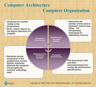
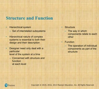
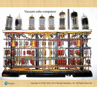
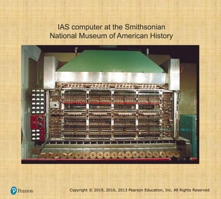
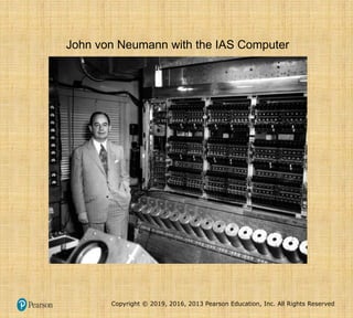
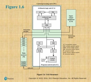
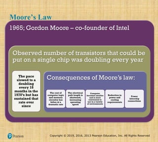
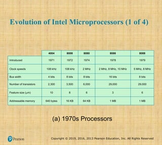
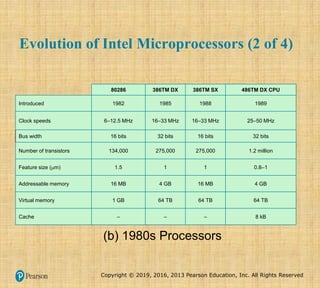
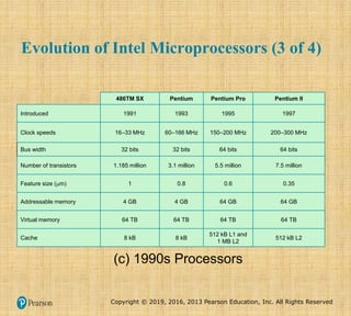
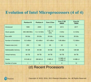
Copyright © 2019, 2016, 2013 Pearson Education, Inc. All Rights Reserved
Computer Organization and Architecture
Designing for Performance
11th Edition
Chapter 1
Basic Concepts and
Computer Evolution
Copyright © 2019, 2016, 2013 Pearson Education, Inc. All Rights Reserved
Computer Architecture
Computer Organization
• The operational units
and their
interconnections that
realize the architectural
specifications
• Hardware details
transparent to the
programmer, control
signals, interfaces
between the computer
and peripherals,
memory technology
used
• Instruction set,
number of bits used to
represent various data
types, I/O
mechanisms,
techniques for
addressing memory
• Attributes of a system
visible to the
programmer
• Have a direct impact on
the logical execution of a
program
Computer
Architecture
Architectural
attributes
include:
Computer
Organization
Organizational
attributes
include:
Copyright © 2019, 2016, 2013 Pearson Education, Inc. All Rights Reserved
Structure and Function
• Hierarchical system
– Set of interrelated subsystems
• Hierarchical nature of complex
systems is essential to both their
design and their description
• Designer need only deal with a
particular
level of the system at a time
– Concerned with structure and
function
at each level
• Structure
– The way in which
components relate to each
other
• Function
– The operation of individual
components as part of the
structure
Copyright © 2019, 2016, 2013 Pearson Education, Inc. All Rights Reserved
Function
• There are four basic functions that a computer can perform:
– Data processing
▪ Data may take a wide variety of forms and the range of processing
requirements is broad
– Data storage
▪ Short-term
▪ Long-term
– Data movement
▪ Input-output (I/O) - when data are received from or delivered to a device
(peripheral) that is directly connected to the computer
▪ Data communications – when data are moved over longer distances, to or from
a remote device
– Control
▪ A control unit manages the computer’s resources and orchestrates the
performance of its functional parts in response to instructions
Copyright © 2019, 2016, 2013 Pearson Education, Inc. All Rights Reserved
Structure
Figure 1.1 A Top-Down View of a Computer
Main
memory
I/O
CPU
COMPUTER
System
Bus
ALU
Registers
Control
Unit
CPU
Internal
Bus
Control Unit
Registers and
Decoders
CONTROL
UNIT
Sequencing
Logic
Control
Memory
Figure 1.1 The Computer: Top-Level Structure
Copyright © 2019, 2016, 2013 Pearson Education, Inc. All Rights Reserved
There are four main structural components
of the computer:
• CPU – controls the operation of the computer and
performs its data processing functions
• Main Memory – stores data
• I/O – moves data between the computer and its external
environment
• System Interconnection – some mechanism that
provides for communication among CPU, main memory,
and I/O
Copyright © 2019, 2016, 2013 Pearson Education, Inc. All Rights Reserved
CPU
Major structural components:
• Control Unit
– Controls the operation of the CPU and hence the computer
• Arithmetic and Logic Unit (ALU)
– Performs the computer’s data processing function
• Registers
– Provide storage internal to the CPU
• CPU Interconnection
– Some mechanism that provides for communication among the
control unit, ALU, and registers
Copyright © 2019, 2016, 2013 Pearson Education, Inc. All Rights Reserved
Multicore Computer Structure
• Central processing unit (CPU)
– Portion of the computer that fetches and executes instructions
– Consists of an ALU, a control unit, and registers
– Referred to as a processor in a system with a single processing unit
• Core
– An individual processing unit on a processor chip
– May be equivalent in functionality to a CPU on a single-CPU system
– Specialized processing units are also referred to as cores
• Processor
– A physical piece of silicon containing one or more cores
– Is the computer component that interprets and executes instructions
– Referred to as a multicore processor if it contains multiple cores
Copyright © 2019, 2016, 2013 Pearson Education, Inc. All Rights Reserved
Cache Memory
• Multiple layers of memory between the processor and main
memory
• Is smaller and faster than main memory
• Used to speed up memory access by placing in the cache data
from main memory that is likely to be used in the near future
• A greater performance improvement may be obtained by using
multiple levels of cache, with level 1 (L1) closest to the core and
additional levels (L2, L3, etc.) progressively farther from the core
Copyright © 2019, 2016, 2013 Pearson Education, Inc. All Rights Reserved
Figure 1.2 Simplified View of Major Elements of a Multicore Computer
MOTHERBOARD
PROCESSOR CHIP
CORE
Processor
chip
Main memory chips
I/O chips
Core
L3 cache
Instruction
logic
L1 I-cache
L2 instruction
cache
L2 data
cache
L1 data cache
Arithmetic
and logic
unit (ALU)
Load/
store logic
L3 cache
Core Core Core
Core Core Core Core
Figure 1.2
Copyright © 2019, 2016, 2013 Pearson Education, Inc. All Rights Reserved
Figure 1.3
Motherboard with Two Intel Quad-Core
Xeon Processors
Source: Courtesy of Chassis Plans Rugged Rackmount Computers
Copyright © 2019, 2016, 2013 Pearson Education, Inc. All Rights Reserved
Figure 1.4
Copyright © 2019, 2016, 2013 Pearson Education, Inc. All Rights Reserved
Figure 1.5
Copyright © 2019, 2016, 2013 Pearson Education, Inc. All Rights Reserved
History of Computers
First Generation: Vacuum Tubes
• Vacuum tubes were used for digital logic elements and memory
• IAS computer
– Fundamental design approach was the stored program
concept
▪ Attributed to the mathematician John von Neumann
▪ First publication of the idea was in 1945 for the EDVAC
– Design began at the Princeton Institute for Advanced Studies
– Completed in 1952
– Prototype of all subsequent general-purpose computers
Copyright © 2019, 2016, 2013 Pearson Education, Inc. All Rights Reserved
Vacuum cube computers
Copyright © 2019, 2016, 2013 Pearson Education, Inc. All Rights Reserved
IAS computer at the Smithsonian
National Museum of American History
Copyright © 2019, 2016, 2013 Pearson Education, Inc. All Rights Reserved
John von Neumann with the IAS Computer
Copyright © 2019, 2016, 2013 Pearson Education, Inc. All Rights Reserved
Control
circuits
Addresses
Control
signals
Instructions
and data
AC: Accumulator register
MQ: multiply-quotient register
MBR: memory buffer register
IBR: instruction buffer register
PC: program counter
MAR: memory address register
IR: insruction register
Instructions
and data
M(0)
M(1)
M(2)
M(3)
M(4)
M(4095)
M(4093)
M(4092)
MBR
Arithmetic-logic unit (CA)
Central processing unit (CPU)
Program control unit (CC)
Figure 1.6 IAS Structure
Input-
output
equipment
(I, O)
Main
memory
(M)
AC MQ
Arithmetic-logic
circuits
IBR
PC
IR
MAR
Figure 1.6
Copyright © 2019, 2016, 2013 Pearson Education, Inc. All Rights Reserved
(a) Number word
sign bit
0 39
(b) Instruction word
Figure 1.7 IAS Memory Formats
opcode (8 bits) address (12 bits)
left instruction (20 bits)
0 8 20 28 39
1
right instruction (20 bits)
opcode (8 bits) address (12 bits)
Figure 1.7
Copyright © 2019, 2016, 2013 Pearson Education, Inc. All Rights Reserved
Registers
• Contains a word to be stored in memory or sent to the I/O unit
• Or is used to receive a word from memory or from the I/O unit
Memory buffer register
(MBR)
• Specifies the address in memory of the word to be written from
or read into the MBR
Memory address
register (MAR)
• Contains the 8-bit opcode instruction being executed
Instruction register (IR)
• Employed to temporarily hold the right-hand instruction from a
word in memory
Instruction buffer
register (IBR)
• Contains the address of the next instruction pair to be fetched
from memory
Program counter (PC)
• Employed to temporarily hold operands and results of ALU
operations
Accumulator (AC) and
multiplier quotient (MQ)
Copyright © 2019, 2016, 2013 Pearson Education, Inc. All Rights Reserved
Start
Is next
instruction
in IBR?
MAR PC
MBR M(MAR)
IR IBR (0:7)
MAR IBR (8:19)
IR MBR (20:27)
MAR MBR (28:39)
Left
instruction
required?
IBR MBR (20:39)
IR MBR (0:7)
MAR MBR (8:19)
PC PC + 1
Yes
Yes
Yes
No
No
No
M(X) = contents of memory location whose addr ess is X
(i:j) = bits i through j
No memory
access
required
Decode instruction in IR
AC M(X) Go to M(X, 0:19) If AC > 0 then
go to M(X, 0:19)
AC AC + M(X)
Is AC > 0?
MBR M(MAR) MBR M(MAR)
PC MAR
AC MBR AC AC + MBR
Fetch
cycle
Execution
cycle
Figure 1.8 Partial Flowchart of IAS Operation
Figure 1.8
Copyright © 2019, 2016, 2013 Pearson Education, Inc. All Rights Reserved
Instruction
Type
Opcode
Symbolic
Representation Description
Data transfer
00001010 LOAD MQ Transfer contents of register MQ to the accumulator AC
00001001 LOAD MQ,M(X) Transfer contents of memory location X to MQ
00100001 STOR M(X) Transfer contents of accumulator to memory location X
00000001 LOAD M(X) Transfer M(X) to the accumulator
00000010 LOAD –M(X) Transfer –M(X) to the accumulator
00000011 LOAD |M(X)| Transfer absolute value of M(X) to the accumulator
00000100 LOAD –|M(X)| Transfer –|M(X)| to the accumulator
Unconditional
branch
00001101 JUMP M(X,0:19) Take next instruction from left half of M(X)
00001110 JUMP M(X,20:39) Take next instruction from right half of M(X)
Conditional
Branch
00001111 JUMP + M(X,0:19) Take next instruction from right half of M(X)
00010000 JUMP + M(X,20:39) If number in the accumulator is nonnegative, take next
instruction from right half of M(X)
Arithmetic
00000101 ADD M(X) Add M(X) to AC; put the result in AC
00000111 ADD |M(X)| Add |M(X)| to AC; put the result in AC
00000110 SUB M(X) Subtract M(X) from AC; put the result in AC
00001000 SUB |M(X)| Subtract |M(X)| from AC; put the remainder in AC
00001011 MUL M(X) Multiply M(X) by MQ; put most significant bits of result
in AC, put least significant bits in MQ
00001100 DIV M(X) Divide AC by M(X); put the quotient in MQ and the
remainder in AC
00010100 LSH Multiply accumulator by 2; that is, shift left one bit position
00010101 RSH Divide accumulator by 2; that is, shift right one position
Address
modify
00010010 STOR M(X,8:19) Replace left address field at M(X) by 12 rightmost bits
of AC
00010011 STOR M(X,28:39) Replace right address field at M(X) by 12 rightmost bits
of AC
(Table can be found on page 16 in the textbook.)
Table 1.1 The IAS Instruction Set
Copyright © 2019, 2016, 2013 Pearson Education, Inc. All Rights Reserved
Boolean
logic
function
Input
Activate
signal
(a) Gate
Figure 1.9 Fundamental Computer Elements
Output
Binary
storage
cell
Input
Read
Write
(b) Memory cell
Output
Figure 1.9
Copyright © 2019, 2016, 2013 Pearson Education, Inc. All Rights Reserved
Transistors
• The fundamental building block of digital circuits used to construct
processors, memories, and other digital logic devices
• Active part of the transistor is made of silicon or some other
semiconductor material that can change its electrical state when
pulsed
– In its normal state the material may be nonconductive or conductive
– The transistor changes its state when voltage is applied to the gate
• Discrete component
– A single, self-contained transistor
– Were manufactured separately, packaged in their own containers, and soldered
or wired together onto Masonite-like circuit boards
Copyright © 2019, 2016, 2013 Pearson Education, Inc. All Rights Reserved
Integrated Circuits
• A computer consists of gates, memory cells, and
interconnections among these elements
• The gates and memory cells are constructed of
simple digital electronic components
• Data storage – provided by
memory cells
• Data processing – provided by
gates
• Data movement – the paths
among components are used to
move data from memory to
memory and from memory
through gates to memory
• Control – the paths among
components can carry control
signals
• Exploits the fact that such components as
transistors, resistors, and conductors can be
fabricated from a semiconductor such as
silicon
• Many transistors can be produced at the
same time on a single wafer of silicon
• Transistors can be connected with a
processor metallization to form circuits
Copyright © 2019, 2016, 2013 Pearson Education, Inc. All Rights Reserved
Wafer
Chip
Gate
Figure 1.10 Relationship Among Wafer, Chip, and Gate
Packaged
chip
Figure 1.10
Copyright © 2019, 2016, 2013 Pearson Education, Inc. All Rights Reserved
Figure 1.11 Processor or Memory Chip on Motherboard
(a) Close-up of packaged chip (b) Chip on motherboard
Figure 1.11
Copyright © 2019, 2016, 2013 Pearson Education, Inc. All Rights Reserved
Figure 1.12 Growth in Transistor Count on Integrated Circuits
(DRAM memory)
1
1947
F
i
r
s
t
w
o
r
k
i
n
g
t
r
a
n
s
i
s
t
o
r
M
o
o
r
e
’
s
l
a
w
p
r
o
m
u
l
g
a
t
e
d
I
n
v
e
n
t
i
o
n
o
f
i
n
t
e
g
r
a
t
e
d
c
i
r
c
u
i
t
50 55 60 65 70 75 80 85 90 95 2000 05 11
10
100
1,000
10.000
100,000
10 m
100 m
1 bn
10 bn
100 bn
Figure 1.12
Copyright © 2019, 2016, 2013 Pearson Education, Inc. All Rights Reserved
Moore’s Law
1965; Gordon Moore – co-founder of Intel
Observed number of transistors that could be
put on a single chip was doubling every year
The pace
slowed to a
doubling
every 18
months in the
1970’s but has
sustained that
rate ever
since
Consequences of Moore’s law:
The cost of
computer logic
and memory
circuitry has
fallen at a
dramatic rate
The electrical
path length is
shortened,
increasing
operating
speed
Computer
becomes smaller
and is more
convenient to
use in a variety
of environments
Reduction in
power and
cooling
requirements
Fewer
interchip
connections
Copyright © 2019, 2016, 2013 Pearson Education, Inc. All Rights Reserved
Figure 1.13
Copyright © 2019, 2016, 2013 Pearson Education, Inc. All Rights Reserved
Evolution of Intel Microprocessors (1 of 4)
4004 8008 8080 8086 8088
Introduced 1971 1972 1974 1978 1979
Clock speeds 108 kHz 108 kHz 2 MHz 2 MHz, 8 MHz, 10 MHz 5 MHz, 8 MHz
Bus width 4 bits 8 bits 8 bits 16 bits 8 bits
Number of transistors 2,300 3,500 6,000 29,000 29,000
Feature size (m) 10 8 6 3 6
Addressable memory 640 bytes 16 KB 64 KB 1 MB 1 MB
(a) 1970s Processors
Copyright © 2019, 2016, 2013 Pearson Education, Inc. All Rights Reserved
Evolution of Intel Microprocessors (2 of 4)
80286 386TM DX 386TM SX 486TM DX CPU
Introduced 1982 1985 1988 1989
Clock speeds 6–12.5 MHz 16–33 MHz 16–33 MHz 25–50 MHz
Bus width 16 bits 32 bits 16 bits 32 bits
Number of transistors 134,000 275,000 275,000 1.2 million
Feature size (m) 1.5 1 1 0.8–1
Addressable memory 16 MB 4 GB 16 MB 4 GB
Virtual memory 1 GB 64 TB 64 TB 64 TB
Cache – – – 8 kB
(b) 1980s Processors
Copyright © 2019, 2016, 2013 Pearson Education, Inc. All Rights Reserved
Evolution of Intel Microprocessors (3 of 4)
486TM SX Pentium Pentium Pro Pentium II
Introduced 1991 1993 1995 1997
Clock speeds 16–33 MHz 60–166 MHz 150–200 MHz 200–300 MHz
Bus width 32 bits 32 bits 64 bits 64 bits
Number of transistors 1.185 million 3.1 million 5.5 million 7.5 million
Feature size (m) 1 0.8 0.6 0.35
Addressable memory 4 GB 4 GB 64 GB 64 GB
Virtual memory 64 TB 64 TB 64 TB 64 TB
Cache 8 kB 8 kB
512 kB L1 and
1 MB L2
512 kB L2
(c) 1990s Processors
Copyright © 2019, 2016, 2013 Pearson Education, Inc. All Rights Reserved
Evolution of Intel Microprocessors (4 of 4)
Pentium III Pentium 4 Core 2 Duo
Core i7 EE
4960X
Core i9-
7900X
Introduced 1999 2000 2006 2013 2017
Clock speeds 450–660 MHz 1.3–1.8 GHz
1.06–1.2
GHz
4 GHz 4.3 GHz
Bus width 64 bits 64 bits 64 bits 64 bits 64 bits
Number of transistors 9.5 million 42 million 167 million 1.86 billion 7.2 billion
Feature size (nm) 250 180 65 22 14
Addressable memory 64 GB 64 GB 64 GB 64 GB 128 GB
Virtual memory 64 TB 64 TB 64 TB 64 TB 64 TB
Cache 512 kB L2 256 kB L2 2 MB L2
1.5 MB L2/
1.5 MB L3
14 MB L3
Number of cores 1 1 2 6 10
(d) Recent Processors
Copyright © 2019, 2016, 2013 Pearson Education, Inc. All Rights Reserved
Highlights of the Evolution of the Intel
Product Line: (1 of 2)
8080
• World’s first
general-
purpose
microprocessor
• 8-bit machine,
8-bit data path
to memory
• Was used in the
first personal
computer
(Altair)
8086
• A more
powerful 16-bit
machine
• Has an
instruction
cache, or
queue, that
prefetches a
few instructions
before they are
executed
• The first
appearance of
the x86
architecture
• The 8088 was a
variant of this
processor and
used in IBM’s
first personal
computer
(securing the
success of Intel
80286
• Extension of the
8086 enabling
addressing a
16-MB memory
instead of just
1MB
80386
• Intel’s first 32-
bit machine
• First Intel
processor to
support
multitasking
80486
• Introduced the
use of much
more
sophisticated
and powerful
cache
technology and
sophisticated
instruction
pipelining
• Also offered a
built-in math
coprocessor
Copyright © 2019, 2016, 2013 Pearson Education, Inc. All Rights Reserved
Highlights of the Evolution of the Intel Product
Line: (2 of 2)
• Intel introduced the use of superscalar techniques, which allow multiple instructions to execute in parallel
Pentium
• Continued the move into superscalar organization with aggressive use of register renaming, branch
prediction, data flow analysis, and speculative execution
Pentium Pro
• Incorporated Intel MMX technology, which is designed specifically to process video, audio, and graphics
data efficiently
Pentium II
•Incorporated additional floating-point instructions
•Streaming SIMD Extensions (SSE)
Pentium III
• Includes additional floating-point and other enhancements for multimedia
Pentium 4
• First Intel x86 micro-core
Core
• Extends the Core architecture to 64 bits
• Core 2 Quad provides four cores on a single chip
• More recent Core offerings have up to 10 cores per chip
• An important addition to the architecture was the Advanced Vector Extensions instruction set
Core 2
Copyright © 2019, 2016, 2013 Pearson Education, Inc. All Rights Reserved
Embedded Systems
• The use of electronics and software within a product
• Billions of computer systems are produced each year that are
embedded within larger devices
• Today many devices that use electric power have an embedded
computing system
• Often embedded systems are tightly coupled to their environment
– This can give rise to real-time constraints imposed by the need to interact with the
environment
▪ Constraints such as required speeds of motion, required precision of
measurement, and required time durations, dictate the timing of software
operations
– If multiple activities must be managed simultaneously this imposes more complex
real-time constraints
Copyright © 2019, 2016, 2013 Pearson Education, Inc. All Rights Reserved
Memory
Custom
logic
Human
interface
Diagnostic
port
Processor
D/A
Conversion
Actuators/
indicators
A/D
conversion
Sensors
Figure 1.14 Possible Organization of an Embedded System
Figure 1.14
Copyright © 2019, 2016, 2013 Pearson Education, Inc. All Rights Reserved
The Internet of Things (IoT)
• Term that refers to the expanding interconnection of smart devices, ranging from
appliances to tiny sensors
• Is primarily driven by deeply embedded devices
• Generations of deployment culminating in the IoT:
– Information technology (IT)
▪ PCs, servers, routers, firewalls, and so on, bought as IT devices by enterprise IT people
and primarily using wired connectivity
– Operational technology (OT)
▪ Machines/appliances with embedded IT built by non-IT companies, such as medical
machinery, SCADA, process control, and kiosks, bought as appliances by enterprise OT
people and primarily using wired connectivity
– Personal technology
▪ Smartphones, tablets, and eBook readers bought as IT devices by consumers exclusively
using wireless connectivity and often multiple forms of wireless connectivity
– Sensor/actuator technology
▪ Single-purpose devices bought by consumers, IT, and OT people exclusively using
wireless connectivity, generally of a single form, as part of larger systems
• It is the fourth generation that is usually thought of as the IoT and it is marked by the
use of billions of embedded devices
Copyright © 2019, 2016, 2013 Pearson Education, Inc. All Rights Reserved
Embedded
Operating
Systems
• There are two general
approaches to developing an
embedded operating system
(OS):
– Take an existing OS and adapt it
for the embedded application
– Design and implement an OS
intended solely for embedded use
• Application processors
– Defined by the processor’s ability to
execute complex operating systems
– General-purpose in nature
– An example is the smartphone – the
embedded system is designed to
support numerous apps and perform
a wide variety of functions
• Dedicated processor
– Is dedicated to one or a small
number of specific tasks required by
the host device
– Because such an embedded system
is dedicated to a specific task or
tasks, the processor and associated
components can be engineered to
reduce size and cost
Application Processors
versus
Dedicated Processors
Copyright © 2019, 2016, 2013 Pearson Education, Inc. All Rights Reserved
Figure 1.15 Typical Microcontroller Chip Elements
A/D
converter
Analog data
acquisition
Temporary
data
Processor
System
bus
RAM
D/A
converter
ROM
Serial I/O
ports
EEPROM
Parallel I/O
ports
TIMER
Program
and data
Permanent
data
Timing
functions
Analog data
transmission
Send/receive
data
Peripheral
interfaces
Figure 1.15
Copyright © 2019, 2016, 2013 Pearson Education, Inc. All Rights Reserved
Deeply Embedded Systems
• Subset of embedded systems
• Has a processor whose behavior is difficult to observe both by the programmer and
the user
• Uses a microcontroller rather than a microprocessor
• Is not programmable once the program logic for the device has been burned into
ROM
• Has no interaction with a user
• Dedicated, single-purpose devices that detect something in the environment,
perform a basic level of processing, and then do something with the results
• Often have wireless capability and appear in networked configurations, such as
networks of sensors deployed over a large area
• Typically have extreme resource constraints in terms of memory, processor size,
time, and power consumption
Copyright © 2019, 2016, 2013 Pearson Education, Inc. All Rights Reserved
ARM
Refers to a processor architecture that has evolved from
RISC design principles and is used in embedded systems
Family of RISC-based microprocessors and microcontrollers
designed by ARM Holdings, Cambridge, England
Chips are high-speed processors that are known for their
small die size and low power requirements
Probably the most widely used embedded processor
architecture and indeed the most widely used processor
architecture of any kind in the world
Acorn RISC Machine/Advanced RISC Machine
Copyright © 2019, 2016, 2013 Pearson Education, Inc. All Rights Reserved
ARM Products
Cortex-A
Cortex-R
Cortex-M
• Cortex-M0
• Cortex-M0+
• Cortex-M3
• Cortex-M4
• Cortex-M7
• Cortex-M23
• Cortex-M33
Copyright © 2019, 2016, 2013 Pearson Education, Inc. All Rights Reserved
Figure 1.16 Typical Microcontroller Chip Based on Cortex-M3
Cortex-M3 Core
Microcontroller Chip
Cortex-M3
Processor
NVIC
interface
ETM
interface
Hardware
divider
32-bit
multiplier
32-bit ALU
Control
logic
Thumb
decode
Instruction
interface
Data
interface
ICode
interface
Debug logic
ARM
core
DAP
NVIC ETM
Memory
protection unit
Bus matrix
SRAM &
peripheral I/F
Security Analog Interfaces Timers &Triggers Parallel I/O Ports Serial Interfaces
Peripheral bus
Core and memory
Clock management
Energy management
Cortex-M3 processor
Memory
protec-
tion unit
Flash
memory
64 kB
Voltage
regula-
tor
Power-
on reset
Brown-
out de-
tector
Voltage
compar-
ator
High fre-
quency RC
oscillator
Low fre-
quency RC
oscillator
High freq
crystal
oscillator
Low freq
crystal
oscillator
SRAM
memory
64 kB
Debug
inter-
face
DMA
control-
ler
Pulse
counter
Watch-
dog tmr
Low
energy
Real
time ctr
Periph
bus int
Timer/
counter
General
purpose
I/O
External
Inter-
rupts
UART
USART
Low-
energy
UART
USB
Pin
reset
32-bit bus
A/D
con-
verter
Hard-
ware
AES
D/A
con-
verter
Figure 1.16
Copyright © 2019, 2016, 2013 Pearson Education, Inc. All Rights Reserved
Summary
Chapter 1
• Organization and architecture
• Structure and function
• The IAS computer
• Gates, memory cells, chips, and
multichip modules
– Gates and memory cells
– Transistors
– Microelectronic chips
– Multichip module
• The evolution of the Intel x86
architecture
Basic Concepts and
Computer Evolution
• Embedded systems
– The Internet of things
– Embedded operating systems
– Application processors versus
dedicated processors
– Microprocessors versus
microcontrollers
– Embedded versus deeply embedded
systems
• ARM architecture
– ARM evolution
– Instruction set architecture
– ARM products
Copyright © 2019, 2016, 2013 Pearson Education, Inc. All Rights Reserved
Copyright
This work is protected by United States copyright laws and is provided solely
for the use of instructions in teaching their courses and assessing student
learning. dissemination or sale of any part of this work (including on the
World Wide Web) will destroy the integrity of the work and is not permit-
ted. The work and materials from it should never be made available to
students except by instructors using the accompanying text in their
classes. All recipients of this work are expected to abide by these
restrictions and to honor the intended pedagogical purposes and the needs of
other instructors who rely on these materials.

CH01-COA11e-revised.pdf

  • 1.
    Copyright © 2019,2016, 2013 Pearson Education, Inc. All Rights Reserved Computer Organization and Architecture Designing for Performance 11th Edition Chapter 1 Basic Concepts and Computer Evolution
  • 2.
    Copyright © 2019,2016, 2013 Pearson Education, Inc. All Rights Reserved Computer Architecture Computer Organization • The operational units and their interconnections that realize the architectural specifications • Hardware details transparent to the programmer, control signals, interfaces between the computer and peripherals, memory technology used • Instruction set, number of bits used to represent various data types, I/O mechanisms, techniques for addressing memory • Attributes of a system visible to the programmer • Have a direct impact on the logical execution of a program Computer Architecture Architectural attributes include: Computer Organization Organizational attributes include:
  • 3.
    Copyright © 2019,2016, 2013 Pearson Education, Inc. All Rights Reserved Structure and Function • Hierarchical system – Set of interrelated subsystems • Hierarchical nature of complex systems is essential to both their design and their description • Designer need only deal with a particular level of the system at a time – Concerned with structure and function at each level • Structure – The way in which components relate to each other • Function – The operation of individual components as part of the structure
  • 4.
    Copyright © 2019,2016, 2013 Pearson Education, Inc. All Rights Reserved Function • There are four basic functions that a computer can perform: – Data processing ▪ Data may take a wide variety of forms and the range of processing requirements is broad – Data storage ▪ Short-term ▪ Long-term – Data movement ▪ Input-output (I/O) - when data are received from or delivered to a device (peripheral) that is directly connected to the computer ▪ Data communications – when data are moved over longer distances, to or from a remote device – Control ▪ A control unit manages the computer’s resources and orchestrates the performance of its functional parts in response to instructions
  • 5.
    Copyright © 2019,2016, 2013 Pearson Education, Inc. All Rights Reserved Structure Figure 1.1 A Top-Down View of a Computer Main memory I/O CPU COMPUTER System Bus ALU Registers Control Unit CPU Internal Bus Control Unit Registers and Decoders CONTROL UNIT Sequencing Logic Control Memory Figure 1.1 The Computer: Top-Level Structure
  • 6.
    Copyright © 2019,2016, 2013 Pearson Education, Inc. All Rights Reserved There are four main structural components of the computer: • CPU – controls the operation of the computer and performs its data processing functions • Main Memory – stores data • I/O – moves data between the computer and its external environment • System Interconnection – some mechanism that provides for communication among CPU, main memory, and I/O
  • 7.
    Copyright © 2019,2016, 2013 Pearson Education, Inc. All Rights Reserved CPU Major structural components: • Control Unit – Controls the operation of the CPU and hence the computer • Arithmetic and Logic Unit (ALU) – Performs the computer’s data processing function • Registers – Provide storage internal to the CPU • CPU Interconnection – Some mechanism that provides for communication among the control unit, ALU, and registers
  • 8.
    Copyright © 2019,2016, 2013 Pearson Education, Inc. All Rights Reserved Multicore Computer Structure • Central processing unit (CPU) – Portion of the computer that fetches and executes instructions – Consists of an ALU, a control unit, and registers – Referred to as a processor in a system with a single processing unit • Core – An individual processing unit on a processor chip – May be equivalent in functionality to a CPU on a single-CPU system – Specialized processing units are also referred to as cores • Processor – A physical piece of silicon containing one or more cores – Is the computer component that interprets and executes instructions – Referred to as a multicore processor if it contains multiple cores
  • 9.
    Copyright © 2019,2016, 2013 Pearson Education, Inc. All Rights Reserved Cache Memory • Multiple layers of memory between the processor and main memory • Is smaller and faster than main memory • Used to speed up memory access by placing in the cache data from main memory that is likely to be used in the near future • A greater performance improvement may be obtained by using multiple levels of cache, with level 1 (L1) closest to the core and additional levels (L2, L3, etc.) progressively farther from the core
  • 10.
    Copyright © 2019,2016, 2013 Pearson Education, Inc. All Rights Reserved Figure 1.2 Simplified View of Major Elements of a Multicore Computer MOTHERBOARD PROCESSOR CHIP CORE Processor chip Main memory chips I/O chips Core L3 cache Instruction logic L1 I-cache L2 instruction cache L2 data cache L1 data cache Arithmetic and logic unit (ALU) Load/ store logic L3 cache Core Core Core Core Core Core Core Figure 1.2
  • 11.
    Copyright © 2019,2016, 2013 Pearson Education, Inc. All Rights Reserved
  • 12.
    Copyright © 2019,2016, 2013 Pearson Education, Inc. All Rights Reserved Figure 1.3 Motherboard with Two Intel Quad-Core Xeon Processors Source: Courtesy of Chassis Plans Rugged Rackmount Computers
  • 13.
    Copyright © 2019,2016, 2013 Pearson Education, Inc. All Rights Reserved Figure 1.4
  • 14.
    Copyright © 2019,2016, 2013 Pearson Education, Inc. All Rights Reserved Figure 1.5
  • 15.
    Copyright © 2019,2016, 2013 Pearson Education, Inc. All Rights Reserved History of Computers First Generation: Vacuum Tubes • Vacuum tubes were used for digital logic elements and memory • IAS computer – Fundamental design approach was the stored program concept ▪ Attributed to the mathematician John von Neumann ▪ First publication of the idea was in 1945 for the EDVAC – Design began at the Princeton Institute for Advanced Studies – Completed in 1952 – Prototype of all subsequent general-purpose computers
  • 16.
    Copyright © 2019,2016, 2013 Pearson Education, Inc. All Rights Reserved Vacuum cube computers
  • 17.
    Copyright © 2019,2016, 2013 Pearson Education, Inc. All Rights Reserved IAS computer at the Smithsonian National Museum of American History
  • 18.
    Copyright © 2019,2016, 2013 Pearson Education, Inc. All Rights Reserved John von Neumann with the IAS Computer
  • 19.
    Copyright © 2019,2016, 2013 Pearson Education, Inc. All Rights Reserved Control circuits Addresses Control signals Instructions and data AC: Accumulator register MQ: multiply-quotient register MBR: memory buffer register IBR: instruction buffer register PC: program counter MAR: memory address register IR: insruction register Instructions and data M(0) M(1) M(2) M(3) M(4) M(4095) M(4093) M(4092) MBR Arithmetic-logic unit (CA) Central processing unit (CPU) Program control unit (CC) Figure 1.6 IAS Structure Input- output equipment (I, O) Main memory (M) AC MQ Arithmetic-logic circuits IBR PC IR MAR Figure 1.6
  • 20.
    Copyright © 2019,2016, 2013 Pearson Education, Inc. All Rights Reserved (a) Number word sign bit 0 39 (b) Instruction word Figure 1.7 IAS Memory Formats opcode (8 bits) address (12 bits) left instruction (20 bits) 0 8 20 28 39 1 right instruction (20 bits) opcode (8 bits) address (12 bits) Figure 1.7
  • 21.
    Copyright © 2019,2016, 2013 Pearson Education, Inc. All Rights Reserved Registers • Contains a word to be stored in memory or sent to the I/O unit • Or is used to receive a word from memory or from the I/O unit Memory buffer register (MBR) • Specifies the address in memory of the word to be written from or read into the MBR Memory address register (MAR) • Contains the 8-bit opcode instruction being executed Instruction register (IR) • Employed to temporarily hold the right-hand instruction from a word in memory Instruction buffer register (IBR) • Contains the address of the next instruction pair to be fetched from memory Program counter (PC) • Employed to temporarily hold operands and results of ALU operations Accumulator (AC) and multiplier quotient (MQ)
  • 22.
    Copyright © 2019,2016, 2013 Pearson Education, Inc. All Rights Reserved Start Is next instruction in IBR? MAR PC MBR M(MAR) IR IBR (0:7) MAR IBR (8:19) IR MBR (20:27) MAR MBR (28:39) Left instruction required? IBR MBR (20:39) IR MBR (0:7) MAR MBR (8:19) PC PC + 1 Yes Yes Yes No No No M(X) = contents of memory location whose addr ess is X (i:j) = bits i through j No memory access required Decode instruction in IR AC M(X) Go to M(X, 0:19) If AC > 0 then go to M(X, 0:19) AC AC + M(X) Is AC > 0? MBR M(MAR) MBR M(MAR) PC MAR AC MBR AC AC + MBR Fetch cycle Execution cycle Figure 1.8 Partial Flowchart of IAS Operation Figure 1.8
  • 23.
    Copyright © 2019,2016, 2013 Pearson Education, Inc. All Rights Reserved Instruction Type Opcode Symbolic Representation Description Data transfer 00001010 LOAD MQ Transfer contents of register MQ to the accumulator AC 00001001 LOAD MQ,M(X) Transfer contents of memory location X to MQ 00100001 STOR M(X) Transfer contents of accumulator to memory location X 00000001 LOAD M(X) Transfer M(X) to the accumulator 00000010 LOAD –M(X) Transfer –M(X) to the accumulator 00000011 LOAD |M(X)| Transfer absolute value of M(X) to the accumulator 00000100 LOAD –|M(X)| Transfer –|M(X)| to the accumulator Unconditional branch 00001101 JUMP M(X,0:19) Take next instruction from left half of M(X) 00001110 JUMP M(X,20:39) Take next instruction from right half of M(X) Conditional Branch 00001111 JUMP + M(X,0:19) Take next instruction from right half of M(X) 00010000 JUMP + M(X,20:39) If number in the accumulator is nonnegative, take next instruction from right half of M(X) Arithmetic 00000101 ADD M(X) Add M(X) to AC; put the result in AC 00000111 ADD |M(X)| Add |M(X)| to AC; put the result in AC 00000110 SUB M(X) Subtract M(X) from AC; put the result in AC 00001000 SUB |M(X)| Subtract |M(X)| from AC; put the remainder in AC 00001011 MUL M(X) Multiply M(X) by MQ; put most significant bits of result in AC, put least significant bits in MQ 00001100 DIV M(X) Divide AC by M(X); put the quotient in MQ and the remainder in AC 00010100 LSH Multiply accumulator by 2; that is, shift left one bit position 00010101 RSH Divide accumulator by 2; that is, shift right one position Address modify 00010010 STOR M(X,8:19) Replace left address field at M(X) by 12 rightmost bits of AC 00010011 STOR M(X,28:39) Replace right address field at M(X) by 12 rightmost bits of AC (Table can be found on page 16 in the textbook.) Table 1.1 The IAS Instruction Set
  • 24.
    Copyright © 2019,2016, 2013 Pearson Education, Inc. All Rights Reserved Boolean logic function Input Activate signal (a) Gate Figure 1.9 Fundamental Computer Elements Output Binary storage cell Input Read Write (b) Memory cell Output Figure 1.9
  • 25.
    Copyright © 2019,2016, 2013 Pearson Education, Inc. All Rights Reserved Transistors • The fundamental building block of digital circuits used to construct processors, memories, and other digital logic devices • Active part of the transistor is made of silicon or some other semiconductor material that can change its electrical state when pulsed – In its normal state the material may be nonconductive or conductive – The transistor changes its state when voltage is applied to the gate • Discrete component – A single, self-contained transistor – Were manufactured separately, packaged in their own containers, and soldered or wired together onto Masonite-like circuit boards
  • 26.
    Copyright © 2019,2016, 2013 Pearson Education, Inc. All Rights Reserved Integrated Circuits • A computer consists of gates, memory cells, and interconnections among these elements • The gates and memory cells are constructed of simple digital electronic components • Data storage – provided by memory cells • Data processing – provided by gates • Data movement – the paths among components are used to move data from memory to memory and from memory through gates to memory • Control – the paths among components can carry control signals • Exploits the fact that such components as transistors, resistors, and conductors can be fabricated from a semiconductor such as silicon • Many transistors can be produced at the same time on a single wafer of silicon • Transistors can be connected with a processor metallization to form circuits
  • 27.
    Copyright © 2019,2016, 2013 Pearson Education, Inc. All Rights Reserved Wafer Chip Gate Figure 1.10 Relationship Among Wafer, Chip, and Gate Packaged chip Figure 1.10
  • 28.
    Copyright © 2019,2016, 2013 Pearson Education, Inc. All Rights Reserved Figure 1.11 Processor or Memory Chip on Motherboard (a) Close-up of packaged chip (b) Chip on motherboard Figure 1.11
  • 29.
    Copyright © 2019,2016, 2013 Pearson Education, Inc. All Rights Reserved Figure 1.12 Growth in Transistor Count on Integrated Circuits (DRAM memory) 1 1947 F i r s t w o r k i n g t r a n s i s t o r M o o r e ’ s l a w p r o m u l g a t e d I n v e n t i o n o f i n t e g r a t e d c i r c u i t 50 55 60 65 70 75 80 85 90 95 2000 05 11 10 100 1,000 10.000 100,000 10 m 100 m 1 bn 10 bn 100 bn Figure 1.12
  • 30.
    Copyright © 2019,2016, 2013 Pearson Education, Inc. All Rights Reserved Moore’s Law 1965; Gordon Moore – co-founder of Intel Observed number of transistors that could be put on a single chip was doubling every year The pace slowed to a doubling every 18 months in the 1970’s but has sustained that rate ever since Consequences of Moore’s law: The cost of computer logic and memory circuitry has fallen at a dramatic rate The electrical path length is shortened, increasing operating speed Computer becomes smaller and is more convenient to use in a variety of environments Reduction in power and cooling requirements Fewer interchip connections
  • 31.
    Copyright © 2019,2016, 2013 Pearson Education, Inc. All Rights Reserved Figure 1.13
  • 32.
    Copyright © 2019,2016, 2013 Pearson Education, Inc. All Rights Reserved Evolution of Intel Microprocessors (1 of 4) 4004 8008 8080 8086 8088 Introduced 1971 1972 1974 1978 1979 Clock speeds 108 kHz 108 kHz 2 MHz 2 MHz, 8 MHz, 10 MHz 5 MHz, 8 MHz Bus width 4 bits 8 bits 8 bits 16 bits 8 bits Number of transistors 2,300 3,500 6,000 29,000 29,000 Feature size (m) 10 8 6 3 6 Addressable memory 640 bytes 16 KB 64 KB 1 MB 1 MB (a) 1970s Processors
  • 33.
    Copyright © 2019,2016, 2013 Pearson Education, Inc. All Rights Reserved Evolution of Intel Microprocessors (2 of 4) 80286 386TM DX 386TM SX 486TM DX CPU Introduced 1982 1985 1988 1989 Clock speeds 6–12.5 MHz 16–33 MHz 16–33 MHz 25–50 MHz Bus width 16 bits 32 bits 16 bits 32 bits Number of transistors 134,000 275,000 275,000 1.2 million Feature size (m) 1.5 1 1 0.8–1 Addressable memory 16 MB 4 GB 16 MB 4 GB Virtual memory 1 GB 64 TB 64 TB 64 TB Cache – – – 8 kB (b) 1980s Processors
  • 34.
    Copyright © 2019,2016, 2013 Pearson Education, Inc. All Rights Reserved Evolution of Intel Microprocessors (3 of 4) 486TM SX Pentium Pentium Pro Pentium II Introduced 1991 1993 1995 1997 Clock speeds 16–33 MHz 60–166 MHz 150–200 MHz 200–300 MHz Bus width 32 bits 32 bits 64 bits 64 bits Number of transistors 1.185 million 3.1 million 5.5 million 7.5 million Feature size (m) 1 0.8 0.6 0.35 Addressable memory 4 GB 4 GB 64 GB 64 GB Virtual memory 64 TB 64 TB 64 TB 64 TB Cache 8 kB 8 kB 512 kB L1 and 1 MB L2 512 kB L2 (c) 1990s Processors
  • 35.
    Copyright © 2019,2016, 2013 Pearson Education, Inc. All Rights Reserved Evolution of Intel Microprocessors (4 of 4) Pentium III Pentium 4 Core 2 Duo Core i7 EE 4960X Core i9- 7900X Introduced 1999 2000 2006 2013 2017 Clock speeds 450–660 MHz 1.3–1.8 GHz 1.06–1.2 GHz 4 GHz 4.3 GHz Bus width 64 bits 64 bits 64 bits 64 bits 64 bits Number of transistors 9.5 million 42 million 167 million 1.86 billion 7.2 billion Feature size (nm) 250 180 65 22 14 Addressable memory 64 GB 64 GB 64 GB 64 GB 128 GB Virtual memory 64 TB 64 TB 64 TB 64 TB 64 TB Cache 512 kB L2 256 kB L2 2 MB L2 1.5 MB L2/ 1.5 MB L3 14 MB L3 Number of cores 1 1 2 6 10 (d) Recent Processors
  • 36.
    Copyright © 2019,2016, 2013 Pearson Education, Inc. All Rights Reserved Highlights of the Evolution of the Intel Product Line: (1 of 2) 8080 • World’s first general- purpose microprocessor • 8-bit machine, 8-bit data path to memory • Was used in the first personal computer (Altair) 8086 • A more powerful 16-bit machine • Has an instruction cache, or queue, that prefetches a few instructions before they are executed • The first appearance of the x86 architecture • The 8088 was a variant of this processor and used in IBM’s first personal computer (securing the success of Intel 80286 • Extension of the 8086 enabling addressing a 16-MB memory instead of just 1MB 80386 • Intel’s first 32- bit machine • First Intel processor to support multitasking 80486 • Introduced the use of much more sophisticated and powerful cache technology and sophisticated instruction pipelining • Also offered a built-in math coprocessor
  • 37.
    Copyright © 2019,2016, 2013 Pearson Education, Inc. All Rights Reserved Highlights of the Evolution of the Intel Product Line: (2 of 2) • Intel introduced the use of superscalar techniques, which allow multiple instructions to execute in parallel Pentium • Continued the move into superscalar organization with aggressive use of register renaming, branch prediction, data flow analysis, and speculative execution Pentium Pro • Incorporated Intel MMX technology, which is designed specifically to process video, audio, and graphics data efficiently Pentium II •Incorporated additional floating-point instructions •Streaming SIMD Extensions (SSE) Pentium III • Includes additional floating-point and other enhancements for multimedia Pentium 4 • First Intel x86 micro-core Core • Extends the Core architecture to 64 bits • Core 2 Quad provides four cores on a single chip • More recent Core offerings have up to 10 cores per chip • An important addition to the architecture was the Advanced Vector Extensions instruction set Core 2
  • 38.
    Copyright © 2019,2016, 2013 Pearson Education, Inc. All Rights Reserved Embedded Systems • The use of electronics and software within a product • Billions of computer systems are produced each year that are embedded within larger devices • Today many devices that use electric power have an embedded computing system • Often embedded systems are tightly coupled to their environment – This can give rise to real-time constraints imposed by the need to interact with the environment ▪ Constraints such as required speeds of motion, required precision of measurement, and required time durations, dictate the timing of software operations – If multiple activities must be managed simultaneously this imposes more complex real-time constraints
  • 39.
    Copyright © 2019,2016, 2013 Pearson Education, Inc. All Rights Reserved Memory Custom logic Human interface Diagnostic port Processor D/A Conversion Actuators/ indicators A/D conversion Sensors Figure 1.14 Possible Organization of an Embedded System Figure 1.14
  • 40.
    Copyright © 2019,2016, 2013 Pearson Education, Inc. All Rights Reserved The Internet of Things (IoT) • Term that refers to the expanding interconnection of smart devices, ranging from appliances to tiny sensors • Is primarily driven by deeply embedded devices • Generations of deployment culminating in the IoT: – Information technology (IT) ▪ PCs, servers, routers, firewalls, and so on, bought as IT devices by enterprise IT people and primarily using wired connectivity – Operational technology (OT) ▪ Machines/appliances with embedded IT built by non-IT companies, such as medical machinery, SCADA, process control, and kiosks, bought as appliances by enterprise OT people and primarily using wired connectivity – Personal technology ▪ Smartphones, tablets, and eBook readers bought as IT devices by consumers exclusively using wireless connectivity and often multiple forms of wireless connectivity – Sensor/actuator technology ▪ Single-purpose devices bought by consumers, IT, and OT people exclusively using wireless connectivity, generally of a single form, as part of larger systems • It is the fourth generation that is usually thought of as the IoT and it is marked by the use of billions of embedded devices
  • 41.
    Copyright © 2019,2016, 2013 Pearson Education, Inc. All Rights Reserved Embedded Operating Systems • There are two general approaches to developing an embedded operating system (OS): – Take an existing OS and adapt it for the embedded application – Design and implement an OS intended solely for embedded use • Application processors – Defined by the processor’s ability to execute complex operating systems – General-purpose in nature – An example is the smartphone – the embedded system is designed to support numerous apps and perform a wide variety of functions • Dedicated processor – Is dedicated to one or a small number of specific tasks required by the host device – Because such an embedded system is dedicated to a specific task or tasks, the processor and associated components can be engineered to reduce size and cost Application Processors versus Dedicated Processors
  • 42.
    Copyright © 2019,2016, 2013 Pearson Education, Inc. All Rights Reserved Figure 1.15 Typical Microcontroller Chip Elements A/D converter Analog data acquisition Temporary data Processor System bus RAM D/A converter ROM Serial I/O ports EEPROM Parallel I/O ports TIMER Program and data Permanent data Timing functions Analog data transmission Send/receive data Peripheral interfaces Figure 1.15
  • 43.
    Copyright © 2019,2016, 2013 Pearson Education, Inc. All Rights Reserved Deeply Embedded Systems • Subset of embedded systems • Has a processor whose behavior is difficult to observe both by the programmer and the user • Uses a microcontroller rather than a microprocessor • Is not programmable once the program logic for the device has been burned into ROM • Has no interaction with a user • Dedicated, single-purpose devices that detect something in the environment, perform a basic level of processing, and then do something with the results • Often have wireless capability and appear in networked configurations, such as networks of sensors deployed over a large area • Typically have extreme resource constraints in terms of memory, processor size, time, and power consumption
  • 44.
    Copyright © 2019,2016, 2013 Pearson Education, Inc. All Rights Reserved ARM Refers to a processor architecture that has evolved from RISC design principles and is used in embedded systems Family of RISC-based microprocessors and microcontrollers designed by ARM Holdings, Cambridge, England Chips are high-speed processors that are known for their small die size and low power requirements Probably the most widely used embedded processor architecture and indeed the most widely used processor architecture of any kind in the world Acorn RISC Machine/Advanced RISC Machine
  • 45.
    Copyright © 2019,2016, 2013 Pearson Education, Inc. All Rights Reserved ARM Products Cortex-A Cortex-R Cortex-M • Cortex-M0 • Cortex-M0+ • Cortex-M3 • Cortex-M4 • Cortex-M7 • Cortex-M23 • Cortex-M33
  • 46.
    Copyright © 2019,2016, 2013 Pearson Education, Inc. All Rights Reserved Figure 1.16 Typical Microcontroller Chip Based on Cortex-M3 Cortex-M3 Core Microcontroller Chip Cortex-M3 Processor NVIC interface ETM interface Hardware divider 32-bit multiplier 32-bit ALU Control logic Thumb decode Instruction interface Data interface ICode interface Debug logic ARM core DAP NVIC ETM Memory protection unit Bus matrix SRAM & peripheral I/F Security Analog Interfaces Timers &Triggers Parallel I/O Ports Serial Interfaces Peripheral bus Core and memory Clock management Energy management Cortex-M3 processor Memory protec- tion unit Flash memory 64 kB Voltage regula- tor Power- on reset Brown- out de- tector Voltage compar- ator High fre- quency RC oscillator Low fre- quency RC oscillator High freq crystal oscillator Low freq crystal oscillator SRAM memory 64 kB Debug inter- face DMA control- ler Pulse counter Watch- dog tmr Low energy Real time ctr Periph bus int Timer/ counter General purpose I/O External Inter- rupts UART USART Low- energy UART USB Pin reset 32-bit bus A/D con- verter Hard- ware AES D/A con- verter Figure 1.16
  • 47.
    Copyright © 2019,2016, 2013 Pearson Education, Inc. All Rights Reserved Summary Chapter 1 • Organization and architecture • Structure and function • The IAS computer • Gates, memory cells, chips, and multichip modules – Gates and memory cells – Transistors – Microelectronic chips – Multichip module • The evolution of the Intel x86 architecture Basic Concepts and Computer Evolution • Embedded systems – The Internet of things – Embedded operating systems – Application processors versus dedicated processors – Microprocessors versus microcontrollers – Embedded versus deeply embedded systems • ARM architecture – ARM evolution – Instruction set architecture – ARM products
  • 48.
    Copyright © 2019,2016, 2013 Pearson Education, Inc. All Rights Reserved Copyright This work is protected by United States copyright laws and is provided solely for the use of instructions in teaching their courses and assessing student learning. dissemination or sale of any part of this work (including on the World Wide Web) will destroy the integrity of the work and is not permit- ted. The work and materials from it should never be made available to students except by instructors using the accompanying text in their classes. All recipients of this work are expected to abide by these restrictions and to honor the intended pedagogical purposes and the needs of other instructors who rely on these materials.