BİLGİSAYAR ORGANİZASYONU &TASARIMI
Computer Organization & Design
Bölüm 6
TEMEL BİLGİSAYAR
ORGANİZASYONU
İstanbul Üniversitesi
2.
TEMEL BİLGİSAYAR ORGANİZASYONU
veTASARIMI
Komut Kodları
Bilgisayar Saklayıcıları
Bilgisayar Komutları
Zamanlama ve Kontrol
Komut Çevrimi
Bellek Referanslı Komutlar
Giriş-Çıkış ve Kesme
Bütün Bilgisayar Tanımlama
Temel Bilgisayarın Tasarımı
ALU Unitesi Tasarımı
3.
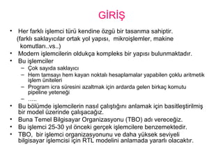
GİRİŞ
• Her farklıişlemci türü kendine özgü bir tasarıma sahiptir.
(farklı saklayıcılar ortak yol yapısı, mikroişlemler, makine
komutları..vs..)
• Modern işlemcilerin oldukça kompleks bir yapısı bulunmaktadır.
• Bu işlemciler
– Çok sayıda saklayıcı
– Hem tamsayı hem kayan noktalı hesaplamalar yapabilen çoklu aritmetik
işlem üniteleri
– Program icra süresini azaltmak için ardarda gelen birkaç komutu
pipeline yeteneği
– …..
• Bu bölümde işlemcilerin nasıl çalıştığını anlamak için basitleştirilmiş
bir model üzerinde çalışacağız.
• Buna Temel Bilgisayar Organizasyonu (TBO) adı vereceğiz.
• Bu işlemci 25-30 yıl önceki gerçek işlemcilere benzemektedir.
• TBO, bir işlemci organizasyonunu ve daha yüksek seviyeli
bilgisayar işlemcisi için RTL modelini anlamada yararlı olacaktır.
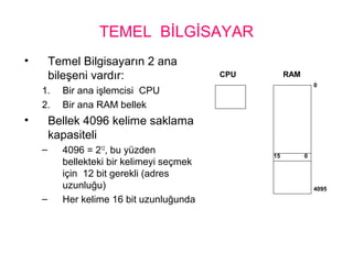
4.
TEMEL BİLGİSAYAR
• TemelBilgisayarın 2 ana
bileşeni vardır:
1. Bir ana işlemcisi CPU
2. Bir ana RAM bellek
• Bellek 4096 kelime saklama
kapasiteli
– 4096 = 212
, bu yüzden
bellekteki bir kelimeyi seçmek
için 12 bit gerekli (adres
uzunluğu)
– Her kelime 16 bit uzunluğunda
CPU RAM
0
4095
015
5.
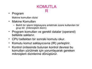
KOMUTLA
R• Program
Makine komutlarıdizisi
• Makine Komutları
– Belirli bir işlemi bilgisayara anlatmak üzere kullanılan bir
grup bit (mikroişlem dizini)
• Program komutları ve gerekli datalar (operand)
bellekte saklanır.
• CPU bellekten bir sonraki komutu okur.
• Komutu komut saklayıcısına (IR) yerleştirir.
• Kontrol ünitesinde bulunan kontrol devresi bu
komutları yürütmek için yorumlayarak gereken
mikroişlem dizinlerine dönüştürür.
6.
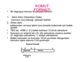
KOMUT
FORMATI• Bir bilgisayarkomutu iki parçaya bölünür:
1. İşlem Alanı (Operation Code)
komutun icra edeceği işlemleri belirler
2. Adres alanı
saklayıcıları ve/veya işlemi icra etmekte kullanmak için bellek
gözleri
• TBO da, 4096 (= 212
) bellek kelimesi 12 bit ile adreslenir
• Komutun en anlamlı biti (15. bit) adresleme modunu belirler.
(0: doğrudan adresleme, 1: dolaylı adresleme)
• Bellek kelimeleri ve komutlar 16 bit uzunluklu oldugundan
komutun işlem alanına 3 bit ayrılmıştır.
Opcode Address
Komut Formatı
15 14 12 0
I
11
Addressing
mode
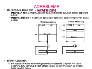
7.
ADRESLEME
MODLARI• Bir komutunadres alanı 2 şekilde belirlenir:
– Doğrudan adresleme: Kullanılan datanın bellekte bulunan adresi (operand
adresi)
– Dolaylı adresleme: Kullanılan operandın bellekteki adresini belirleyen adres
değeri
• Efektif Adres (EA)
– Bir hesaplama türü komutun gerektirdiği operanda ulaşmak için veya
dallanma türü komutun hedef adresi olarak, değiştirmeksizin doğrudan
kullanılabilen adres.
0 ADD 45722
Operand457
1 ADD 30035
1350300
Operand1350
+
AC
+
AC
Direct addressing Indirect addressing
8.
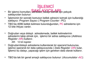
İŞLEMCİ
SAKLAYICILARI• Bir işlemcikomutları, adresleri, datayı tutmak için pekçok
saklayıcıları bulunur:
• İşlemcinin bir sonraki komutun bellek adresini tutmak için kullandığı
saklayıcı: Program Sayacı ( Program Counter - PC)
• TBO’da 4096 bellek kelimesi bulunduğundan, PC adresleme için
12 bite ihtiyac vardır.
• Doğrudan veya dolaylı adreslemede, bellek kelimelerinin
adreslerini takip etmek için, işlemci bir adres saklayıcısı (Address
Register -AR) kullanır.
AR: 12 bit register
• Doğrudan/dolaylı adresleme kullanılarak bir operand bulunursa,
işlemci operandı bir data saklayıcısında ( Data Register -DR) tutar.
İşlemci bu datayı, yapacağı işlem için gereken data olarak kullanır.
• TBO’da tek bir genel amaçlı saklayıcısı bulunur: (Accumulator -AC)
9.
İŞLEMCİ
SAKLAYICILARI• ACC komutlardadoğrudan kullanılır, adresini belirlemeye ihtiyaç
yoktur.
• Örneğin, load AC belirli bir bellek adresinin içeriğini Aküye yükle
• İşlemci ara sonuçları tutmak veya geçici bilgileri saklamak için bir
saklayıcıya gereksinim duyar. TBO’da buna geçici saklayıcı
(Temporary Register -TR) denir.
• TBO çok basit bir giriş/çıkış işlemi (input/output -I/O) kullanır:
Giriş elemanları 8 bits karakter kodlarını işlemciye gönderir.
İşlemci de, 8 bits karakter kodlarını
çıkış elemanına gönderir
• Giriş saklayıcısı (INPR) giriş elemanlarından gelen 8 bit karakter
kodlarını tutar.
• Çıkış saklayıcısı ise (OUTR) bir çıkış elemanına göndermek üzere 8
bit karakter kodları tutar.
10.
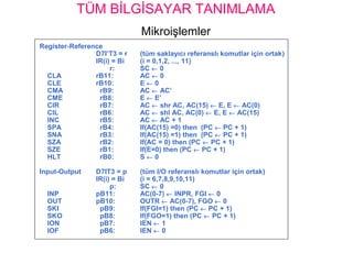
Temel Bilgisayar
Saklayıcıları
Temel BilgisayarSaklayıcıları
DR 16 Data Register Bellek operandını tutar
AR 12 Address Register Bellek için adres tutar.
AC 16 Accumulator İşlemci saklayıcısı
IR 16 Instruction Register Komut kodunu tutar.
PC 12 Program Counter Bir komut adresi tutar
TR 16 Temporary Register Geçici data tutar.
INPR 8 Input Register Giriş karakterini tutar
OUTR 8 Output Register Çıkış karakterini
tutar.
11 0
PC
15 0
IR
15 0
TR
7 0
OUTR
15 0
DR
15 0
AC
11 0
AR
INPR
0 7
Bellek
4096 x 16
CPU
11.
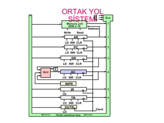
ORTAK YOL
SİSTEMİ
S2
S1
S0
Bus
Memory unit
4096x 16
LD INR CLR
Address
ReadWrite
AR
LD INR CLR
PC
LD INR CLR
DR
LD INR CLR
ACALU
E
INPR
IR
LD
LD INR CLR
TR
OUTR
LD
Clock
16-bit common bus
7
1
2
3
4
5
6
12.
ORTAK YOL
SİSTEMİ
AR
PC
DR
L IC
L I C
L I C
AC
L I C
ALUE
IR
L
TR
L I C
OUTR LD
INPR
Memory
4096 x 16
Address
Read
Write
16-bit Common Bus
7 1 2 3 4 5 6
S0 S1 S2
13.
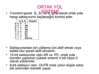
ORTAK YOL
SİSTEMİ• 3kontrol işareti S2, S1, ve S0 giriş olarak ortak yola
hangi saklayıcının seçileceğini kontrol eder.
• Saklayıcılardan biri yükleme izni aktif olmalı veya
bellek oku işareti aktif olmalıdır.
• 12-bit saklayıcılar olan AR ve PC, ortak yola
transfer yaparken yüksek anlamlı 4 biti hepsi 0
olarak yüklenirler.
• 8-bit saklayıcı olan OUTR ortak yolun düşük sekiz
biti üzerinden transfer yapar.
0 0 0 x
0 0 1 AR
0 1 0 PC
0 1 1 DR
1 0 0 AC
1 0 1 IR
1 1 0 TR
1 1 1 Memory
S2 S1 S0 Register
14.
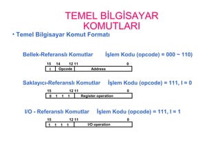
TEMEL BİLGİSAYAR
KOMUTLARI
• TemelBilgisayar Komut Formatı
15 14 12 11 0
I Opcode Address
Bellek-Referanslı Komutlar İşlem Kodu (opcode) = 000 ~ 110)
Saklayıcı-Referanslı Komutlar İşlem Kodu (opcode) = 111, I = 0
I/O - Referanslı Komutlar İşlem Kodu (opcode) = 111, I = 1
15 12 11 0
Register operation0 1 1 1
15 12 11 0
I/O operation1 1 1 1
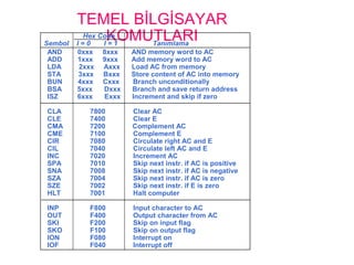
15.
TEMEL BİLGİSAYAR
KOMUTLARIHex Code
SembolI = 0 I = 1 Tanımlama
AND 0xxx 8xxx AND memory word to AC
ADD 1xxx 9xxx Add memory word to AC
LDA 2xxx Axxx Load AC from memory
STA 3xxx Bxxx Store content of AC into memory
BUN 4xxx Cxxx Branch unconditionally
BSA 5xxx Dxxx Branch and save return address
ISZ 6xxx Exxx Increment and skip if zero
CLA 7800 Clear AC
CLE 7400 Clear E
CMA 7200 Complement AC
CME 7100 Complement E
CIR 7080 Circulate right AC and E
CIL 7040 Circulate left AC and E
INC 7020 Increment AC
SPA 7010 Skip next instr. if AC is positive
SNA 7008 Skip next instr. if AC is negative
SZA 7004 Skip next instr. if AC is zero
SZE 7002 Skip next instr. if E is zero
HLT 7001 Halt computer
INP F800 Input character to AC
OUT F400 Output character from AC
SKI F200 Skip on input flag
SKO F100 Skip on output flag
ION F080 Interrupt on
IOF F040 Interrupt off
16.
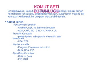
KOMUT SETİ
BÜTÜNLÜĞÜ
• KomutTürleri
Bir bilgisayarın komut seti bütünlüğü, hesaplanabilir olarak bilinen
herhangi bir fonksiyonu değerlendirmek için, kullanıcının makine dili
komutları kullanarak bir program oluşturabilmesidir.
Fonksiyonel Komutlar:
- Aritmetik, lojik, ve öteleme komutları
- ADD, CMA, INC, CIR, CIL, AND, CLA
Transfer Komutları
- Bellek-işlemci saklayıcıları arasındaki data
transferleri.
- LDA, STA
Kontrol komutları
- Program düzenleme ve kontrol
- BUN, BSA, ISZ
Giriş/Çıkış Komutları
- Giriş ve Çıkış
- INP, OUT
17.
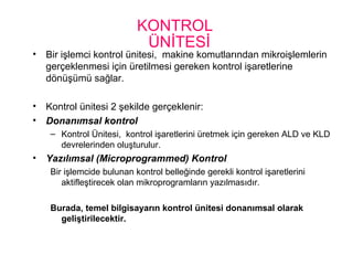
KONTROL
ÜNİTESİ
• Bir işlemcikontrol ünitesi, makine komutlarından mikroişlemlerin
gerçeklenmesi için üretilmesi gereken kontrol işaretlerine
dönüşümü sağlar.
• Kontrol ünitesi 2 şekilde gerçeklenir:
• Donanımsal kontrol
– Kontrol Ünitesi, kontrol işaretlerini üretmek için gereken ALD ve KLD
devrelerinden oluşturulur.
• Yazılımsal (Microprogrammed) Kontrol
Bir işlemcide bulunan kontrol belleğinde gerekli kontrol işaretlerini
aktifleştirecek olan mikroprogramların yazılmasıdır.
Burada, temel bilgisayarın kontrol ünitesi donanımsal olarak
geliştirilecektir.
18.
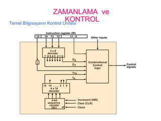
ZAMANLAMA ve
KONTROLTemel BilgisayarınKontrol Ünitesi
Instruction register (IR)
15 14 13 12 11 - 0
3 x 8
decoder
7 6 5 4 3 2 1 0
I
D0
15 14 . . . . 2 1 0
4 x 16
decoder
4-bit
sequence
counter
(SC)
Increment (INR)
Clear (CLR)
Clock
Other inputs
Control
signals
D
T
T
7
15
0
Combinational
Control
logic
KOMUT ÇEVRİMİ
• TemelBilgisayarda, bir makine komutu sırasıyla
aşağıdaki aşamalar halinde icra edilir. :
1. Bellekten komut alma işlemi (fetching)
2. Komutun kodçözümü (decoding)
3. Komut dolaylı adresle kullanıyorsa, bellekten efektif adres
okuma
4. Komut icrası
• Bir komut icra edildikten sonra, bir sonraki komut için,
1. adımdaki çevrim tekrar başlar.
• Not: Her farklı işlemci, kendine özgü ayrı bir komut
çevrimine sahiptir.
21.
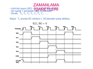
Komut alma (fetch)ve kodçözümü
(decode)• Fetch ve Decode T0: AR ← PC (S0S1S2=010, T0=1)
T1: IR ← M [AR], PC ← PC + 1 (S0S1S2=111, T1=1)
T2: D0, . . . , D7 ← Decode IR(12-14), AR ← IR(0-11), I ← IR(15)
S2
S1
S0
Bus
7
Memory
unit
Address
Read
AR
LD
PC
INR
IR
LD Clock
1
2
5
Common bus
T1
T0
22.
KOMUT TÜRÜNÜN BELİRLENMESİAKIŞI
= 0 (direct)
D'7IT3: AR ← M[AR]
D'7I'T3: Hiçbirşey
D7I'T3: Saklayıcı referanslı komut icrası.
D7IT3: I/O referanslı komut icrası.
Start
SC ← 0
AR ← PC
T0
IR ← M[AR], PC ← PC + 1
T1
AR ← IR(0-11), I ← IR(15)
Decode Opcode in IR(12-14),
T2
D7
= 0 (Memory-reference)(Register or I/O) = 1
II
Execute
register-reference
instruction
SC ← 0
Execute
input-output
instruction
SC ← 0
M[AR]←AR Nothing
= 0 (register)(I/O) = 1 (indirect) = 1
T3 T3 T3 T3
Execute
memory-reference
instruction
SC ← 0
T4
23.
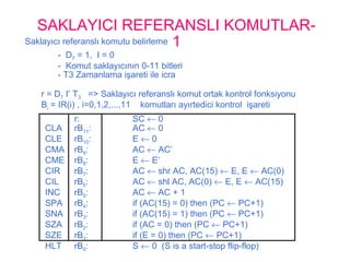
SAKLAYICI REFERANSLI KOMUTLAR-
1
r= D7 I’ T3 => Saklayıcı referanslı komut ortak kontrol fonksiyonu
Bi = IR(i) , i=0,1,2,...,11 komutları ayırtedici kontrol işareti
- D7 = 1, I = 0
- Komut saklayıcının 0-11 bitleri
- T3 Zamanlama işareti ile icra
Saklayıcı referanslı komutu belirleme
r: SC ← 0
CLA rB11: AC ← 0
CLE rB10: E ← 0
CMA rB9: AC ← AC’
CME rB8: E ← E’
CIR rB7: AC ← shr AC, AC(15) ← E, E ← AC(0)
CIL rB6: AC ← shl AC, AC(0) ← E, E ← AC(15)
INC rB5: AC ← AC + 1
SPA rB4: if (AC(15) = 0) then (PC ← PC+1)
SNA rB3: if (AC(15) = 1) then (PC ← PC+1)
SZA rB2: if (AC = 0) then (PC ← PC+1)
SZE rB1: if (E = 0) then (PC ← PC+1)
HLT rB0: S ← 0 (S is a start-stop flip-flop)
24.
BELLEK REFERANSLI KOMUTLAR-
2
ANDto AC
D0T4: DR ← M[AR] Operand oku
D0T5: AC ← AC ∧ DR, SC ← 0 AC içeriği ile AND le
ADD to AC
D1T4: DR ← M[AR] Operand oku
D1T5: AC ← AC + DR, E ← Cout, SC ← 0 AC ile topla ve eldeyi E f.f. ta tut.
-Komut efektif adresi AR saklayıcısındadır ve
-T2 işareti boyunca ( I = 0 iken), T3 işareti boyunca (I = 1 iken)
- Bellek ref. Komut icraları T4 ile başlar.
Symbol
Operation
Decoder
Symbolic Description
AND D0 AC ← AC ∧ M[AR]
ADD D1 AC ← AC + M[AR], E ← Cout
LDA D2 AC ← M[AR]
STA D3 M[AR] ← AC
BUN D4 PC ← AR
BSA D5 M[AR] ← PC, PC ← AR + 1
ISZ D6 M[AR] ← M[AR] + 1, if M[AR] + 1 = 0 then PC ← PC+1
25.
BELLEK REFERANSLI KOMUTLAR-3
İcradansonraki Bellek, PC
21
0 BSA 135
Bir sonraki komut
Altprogram
20
PC = 21
AR = 135
136
1 BUN 135
Bellek, PC, AR ( T4 zamanı)
0 BSA 135
Bir sonraki komut
Alt program
20
21
135
PC = 136
1 BUN 135
Bellek Bellek
LDA: AC ye yükle
D2T4: DR ← M[AR]
D2T5: AC ← DR, SC ← 0
STA: AC yi sakla
D3T4: M[AR] ← AC, SC ← 0
BUN: Şartsız dallan
D4T4: PC ← AR, SC ← 0
BSA: Dallan ve Dönüş adresini sakla
M[AR] ← PC, PC ← AR + 1
26.
BELLEK REFERANSLI KOMUTLAR-4
BSA:
D5T4:M[AR] ← PC, AR ← AR + 1
D5T5: PC ← AR, SC ← 0
ISZ: Bellek İçeriğini artır, içerik=0 ise komut atla
D6T4: DR ← M[AR]
D6T5: DR ← DR + 1
D6T6: M[AR] ← DR, if (DR = 0) then (PC ← PC + 1), SC ← 0
27.
BELLEK REFERANSLI KOMUTLAR
AKIŞIBellekreferanslı komutlar
DR ← M[AR] DR ← M[AR] DR ← M[AR] M[AR] ← AC
SC ← 0
AND ADD LDA STA
AC ← AC DR
SC ← 0
AC ← AC + DR
E ← Cout
SC ← 0
AC ← DR
SC ← 0
D T0 4 D T1 4 D T2 4 D T3 4
D T0 5 D T1 5 D T2 5
PC ← AR
SC ← 0
M[AR] ← PC
AR ← AR + 1
DR ← M[AR]
BUN BSA ISZ
D T4 4 D T5 4 D T6 4
DR ← DR + 1
D T5 5 D T6 5
PC ← AR
SC ← 0
M[AR] ← DR
If (DR = 0)
then (PC ← PC + 1)
SC ← 0
D T6 6
∧
28.
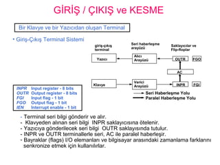
GİRİŞ / ÇIKIŞve KESME
• Giriş-Çıkış Terminal Sistemi
INPR Input register - 8 bits
OUTR Output register - 8 bits
FGI Input flag - 1 bit
FGO Output flag - 1 bit
IEN Interrupt enable - 1 bit
- Terminal seri bilgi gönderir ve alır.
- Klavyeden alınan seri bilgi INPR saklayıcısına ötelenir.
- Yazıcıya gönderilecek seri bilgi OUTR saklayısında tutulur.
- INPR ve OUTR terminallerle seri, AC ile paralel haberleşir.
- Bayraklar (flags) I/O elemanları ve bilgisayar arasındaki zamanlama farklarını
senkronize etmek için kullanılırlar.
Bir Klavye ve bir Yazıcıdan oluşan Terminal
giriş-çıkış
terminal
Seri haberleşme
arayüzü
Saklayıcılar ve
Flip-floplar
Yazıcı
Klavye
Alıcı
Arayüzü
Verici
Arayüzü
FGOOUTR
AC
INPR FGI
Seri Haberleşme Yolu
Paralel Haberleşme Yolu
29.
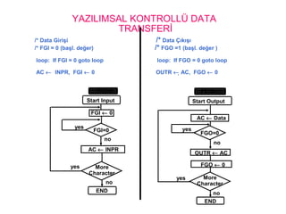
YAZILIMSAL KONTROLLÜ DATA
TRANSFERİ
/*Data Girişi /* Data Çıkışı
/* FGI = 0 (başl. değer) /* FGO =1 (başl. değer )
loop: If FGI = 0 goto loop loop: If FGO = 0 goto loop
AC ← INPR, FGI ← 0 OUTR ← AC, FGO ← 0
Start Input
FGI ← 0
FGI=0
AC ← INPR
More
Character
END
Start Output
FGO ← 0
FGO=0
More
Character
END
OUTR ← AC
AC ← Data
yes
no
yes
no
FGI=0 FGO=1
yes
yes
no
no
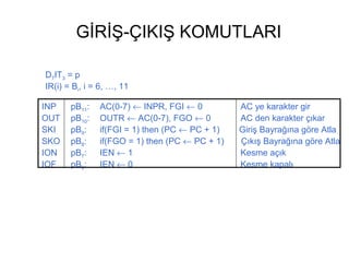
30.
GİRİŞ-ÇIKIŞ KOMUTLARI
D7IT3 =p
IR(i) = Bi, i = 6, …, 11
INP pB11: AC(0-7) ← INPR, FGI ← 0 AC ye karakter gir
OUT pB10: OUTR ← AC(0-7), FGO ← 0 AC den karakter çıkar
SKI pB9: if(FGI = 1) then (PC ← PC + 1) Giriş Bayrağına göre Atla
SKO pB8: if(FGO = 1) then (PC ← PC + 1) Çıkış Bayrağına göre Atla
ION pB7: IEN ← 1 Kesme açık
IOF pB6: IEN ← 0 Kesme kapalı
31.
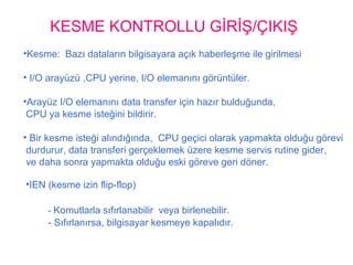
KESME KONTROLLU GİRİŞ/ÇIKIŞ
•Kesme:Bazı dataların bilgisayara açık haberleşme ile girilmesi
• I/O arayüzü ,CPU yerine, I/O elemanını görüntüler.
•Arayüz I/O elemanını data transfer için hazır bulduğunda,
CPU ya kesme isteğini bildirir.
• Bir kesme isteği alındığında, CPU geçici olarak yapmakta olduğu görevi
durdurur, data transferi gerçeklemek üzere kesme servis rutine gider,
ve daha sonra yapmakta olduğu eski göreve geri döner.
•IEN (kesme izin flip-flop)
- Komutlarla sıfırlanabilir veya birlenebilir.
- Sıfırlanırsa, bilgisayar kesmeye kapalıdır.
32.
KESME ÇEVRİMİ
AKIŞI R= Interrupt f/f
Kesme Çevrimi dallan ve dönüş adresini sakla işleminin donanımsal gerçeklemesidir.
Bir sonraki komut çevriminin başlangıcında, bellekten okunan komut 1 nolu adrestedir.
-1 nolu bellek adresinde, programcı kesme servis rutin programına kontrolü yönlendiren
bir dallanma komutu saklamalıdır.
- Orijinal programa kontrolü yönlendiren komut “(dolaylı) I BUN 0“ komutudur.
Store return address
R
=1=0
in location 0
M[0] ← PC
Branch to location 1
PC ← 1
IEN ← 0
R ← 0
Interrupt cycleInstruction cycle
Fetch and decode
instructions
IEN
FGI
FGO
Execute
instructions
R ← 1
=1
=1
=1
=0
=0
=0
33.
KESME ÇEVRİMİNDE
SAKLAYICI TRANSFERİŞLEMLERİ
RTL İfadeleri (Kesme Çevrimi)
- R F/F ← 1 if IEN (FGI + FGO)T0’T1’T2’
⇔ T0’T1’T2’ (IEN)(FGI + FGO): R ← 1
-Komut çevriminin fetch ve decode aşamaları değiştirilmelidir:
T0, T1, T2 yerine R'T0, R'T1, R'T2
- Kesme Çevrimi
RT0: AR ← 0, TR ← PC
RT1: M[AR] ← TR, PC ← 0
RT2: PC ← PC + 1, IEN ← 0, R ← 0, SC ← 0
Kesme çevriminden sonra
0 BUN 1120
0
1
PC = 256
255
1 BUN 0
Kesmeden önce
Main
Program
1120
I/O
Program
0 BUN 1120
0
PC = 1
256
255
1 BUN 0
Memory
Main
Program
1120
I/O
Program
256
34.
TÜM BİLGİSAYAR TANIMLAMA
İşlemlerinAkış Şeması
=1 (I/O) =0 (Register) =1(Indir) =0(Dir)
start
SC ← 0, IEN ← 0, R ← 0
R
AR ← PC
R’T0
IR ← M[AR], PC ← PC + 1
R’T1
AR ← IR(0~11), I ← IR(15)
D0...D7 ← Decode IR(12 ~ 14)
R’T2
AR ← 0, TR ← PC
RT0
M[AR] ← TR, PC ← 0
RT1
PC ← PC + 1, IEN ← 0
R ← 0, SC ← 0
RT2
D7
I I
Execute
I/O
Instruction
Execute
RR
Instruction
AR <- M[AR] Idle
D7IT3 D7I’T3 D7’IT3 D7’I’T3
Execute MR
Instruction
=0(Instruction =1(Interrupt
Cycle) Cycle)
=1(Register or I/O) =0(Memory Ref)
D7’T4
Register-Reference
CLA
CLE
CMA
CME
CIR
CIL
INC
SPA
SNA
SZA
SZE
HLT
Input-Output
INP
OUT
SKI
SKO
ION
IOF
D7I’T3 = r
IR(i)= Bi
r:
rB11:
rB10:
rB9:
rB8:
rB7:
rB6:
rB5:
rB4:
rB3:
rB2:
rB1:
rB0:
D7IT3 = p
IR(i) = Bi
p:
pB11:
pB10:
pB9:
pB8:
pB7:
pB6:
(tüm saklayıcı referanslı komutlar için ortak)
(i = 0,1,2, ..., 11)
SC ← 0
AC ← 0
E ← 0
AC ← AC’
E ← E’
AC ← shr AC, AC(15) ← E, E ← AC(0)
AC ← shl AC, AC(0) ← E, E ← AC(15)
AC ← AC + 1
If(AC(15) =0) then (PC ← PC + 1)
If(AC(15) =1) then (PC ← PC + 1)
If(AC = 0) then (PC ← PC + 1)
If(E=0) then (PC ← PC + 1)
S ← 0
(tüm I/O referanslı komutlar için ortak)
(i = 6,7,8,9,10,11)
SC ← 0
AC(0-7) ← INPR, FGI ← 0
OUTR ← AC(0-7), FGO ← 0
If(FGI=1) then (PC ← PC + 1)
If(FGO=1) then (PC ← PC + 1)
IEN ← 1
IEN ← 0
TÜM BİLGİSAYAR TANIMLAMA
Mikroişlemler
37.
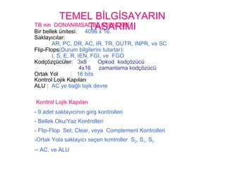
TEMEL BİLGİSAYARIN
TASARIMITB ninDONANIMSAL BİLEŞENLERİ
Bir bellek ünitesi: 4096 x 16.
Saklayıcılar:
AR, PC, DR, AC, IR, TR, OUTR, INPR, ve SC
Flip-Flops(Durum bilgilerini tutarlar):
I, S, E, R, IEN, FGI, ve FGO
Kodçözçücüler: 3x8 Opkod kodçözücü
4x16 zamanlama kodçözücü
Ortak Yol : 16 bits
Kontrol Lojik Kapıları
ALU : AC ye bağlı lojik devre
Kontrol Lojik Kapıları
- 9 adet saklayıcının giriş kontrolleri
- Bellek Oku/Yaz Kontrolleri
- Flip-Flop Set, Clear, veya Complement Kontrolleri
-Ortak Yola saklayıcı seçen kontroller S2, S1, S0
-- AC, ve ALU
38.
SAKLAYICI ve BELLEK
KONTROLLERİ
ARnin içeriğini etkiyen tüm RTL ifadeleri:
LD(AR) = R'T0 + R'T2 + D'7IT3
CLR(AR) = RT0
INR(AR) = D5T4
Adres Saklayıcı; AR
R’T0: AR ← PC LD(AR)
R’T2: AR ← IR(0-11) LD(AR)
D’7IT3: AR ← M[AR] LD(AR)
RT0: AR ← 0 CLR(AR)
D5T4: AR ← AR + 1 INR(AR)
AR
LD
INR
CLR
Clock
To bus
12
From bus
12
D'
I
T
T
R
T
D
T
7
3
2
0
4
39.
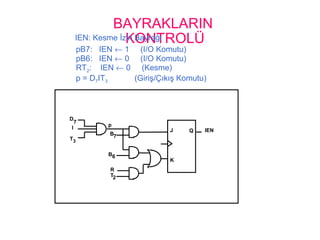
BAYRAKLARIN
KONTROLÜ
pB7: IEN ←1 (I/O Komutu)
pB6: IEN ← 0 (I/O Komutu)
RT2: IEN ← 0 (Kesme)
p = D7IT3 (Giriş/Çıkış Komutu)
IEN: Kesme İzin Bayrağı
D
I
T3
7
J
K
Q IEN
p
B7
B6
T2
R
40.
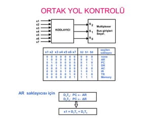
ORTAK YOL KONTROLÜ
ARsaklayıcısı için D4T4: PC ← AR
D5T5: PC ← AR
x1 = D4T4 + D5T5
x1
x2
x3
x4
x5
x6
x7
KODLAYICI
S 2
S 1
S 0
Multiplexer
Bus girişleri
Seçer.
x1 x2 x3 x4 x5 x6 x7 S2 S1 S0
seçilen
saklayıcı
0 0 0 0 0 0 0 0 0 0 none
1 0 0 0 0 0 0 0 0 1 AR
0 1 0 0 0 0 0 0 1 0 PC
0 0 1 0 0 0 0 0 1 1 DR
0 0 0 1 0 0 0 1 0 0 AC
0 0 0 0 1 0 0 1 0 1 IR
0 0 0 0 0 1 0 1 1 0 TR
0 0 0 0 0 0 1 1 1 1 Memory
41.
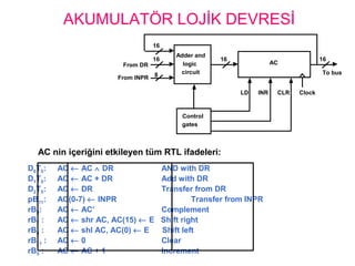
AKUMULATÖR LOJİK DEVRESİ
ACnin içeriğini etkileyen tüm RTL ifadeleri:
16
16
8
Adder and
logic
circuit
16
ACFrom DR
From INPR
Control
gates
LD INR CLR
16
To bus
Clock
D0T5: AC ← AC ∧ DR AND with DR
D1T5: AC ← AC + DR Add with DR
D2T5: AC ← DR Transfer from DR
pB11: AC(0-7) ← INPR Transfer from INPR
rB9: AC ← AC’ Complement
rB7 : AC ← shr AC, AC(15) ← E Shift right
rB6 : AC ← shl AC, AC(0) ← E Shift left
rB11 : AC ← 0 Clear
rB5 : AC ← AC + 1 Increment
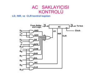
42.
AC SAKLAYICISI
KONTROLÜ
LD, INR,ve CLR kontrol kapıları
AC
LD
INR
CLR
Clock
To bus16From Adder
and Logic
16
AND
ADD
DR
INPR
COM
SHR
SHL
INC
CLR
D0
D1
D2
B11
B9
B7
B6
B5
B11
r
p
T5
T5
43.
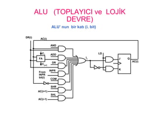
ALU (TOPLAYICI veLOJİK
DEVRE)
ALU’ nun bir katı (i. bit)
AND
ADD
DR
INPR
COM
SHR
SHL
J
K
Q
AC(i)
LD
FA
C
C
From
INPR
bit(i)
DR(i)
AC(i)
AC(i+1)
AC(i-1)
i
i
i+1
I


![Komut alma (fetch) ve kodçözümü
(decode)• Fetch ve Decode T0: AR ← PC (S0S1S2=010, T0=1)
T1: IR ← M [AR], PC ← PC + 1 (S0S1S2=111, T1=1)
T2: D0, . . . , D7 ← Decode IR(12-14), AR ← IR(0-11), I ← IR(15)
S2
S1
S0
Bus
7
Memory
unit
Address
Read
AR
LD
PC
INR
IR
LD Clock
1
2
5
Common bus
T1
T0](https://image.slidesharecdn.com/blm6-150227054934-conversion-gate01/85/Bolum-6-21-320.jpg)
![KOMUT TÜRÜNÜN BELİRLENMESİ AKIŞI
= 0 (direct)
D'7IT3: AR ← M[AR]
D'7I'T3: Hiçbirşey
D7I'T3: Saklayıcı referanslı komut icrası.
D7IT3: I/O referanslı komut icrası.
Start
SC ← 0
AR ← PC
T0
IR ← M[AR], PC ← PC + 1
T1
AR ← IR(0-11), I ← IR(15)
Decode Opcode in IR(12-14),
T2
D7
= 0 (Memory-reference)(Register or I/O) = 1
II
Execute
register-reference
instruction
SC ← 0
Execute
input-output
instruction
SC ← 0
M[AR]←AR Nothing
= 0 (register)(I/O) = 1 (indirect) = 1
T3 T3 T3 T3
Execute
memory-reference
instruction
SC ← 0
T4](https://image.slidesharecdn.com/blm6-150227054934-conversion-gate01/85/Bolum-6-22-320.jpg)
![BELLEK REFERANSLI KOMUTLAR-
2
AND to AC
D0T4: DR ← M[AR] Operand oku
D0T5: AC ← AC ∧ DR, SC ← 0 AC içeriği ile AND le
ADD to AC
D1T4: DR ← M[AR] Operand oku
D1T5: AC ← AC + DR, E ← Cout, SC ← 0 AC ile topla ve eldeyi E f.f. ta tut.
-Komut efektif adresi AR saklayıcısındadır ve
-T2 işareti boyunca ( I = 0 iken), T3 işareti boyunca (I = 1 iken)
- Bellek ref. Komut icraları T4 ile başlar.
Symbol
Operation
Decoder
Symbolic Description
AND D0 AC ← AC ∧ M[AR]
ADD D1 AC ← AC + M[AR], E ← Cout
LDA D2 AC ← M[AR]
STA D3 M[AR] ← AC
BUN D4 PC ← AR
BSA D5 M[AR] ← PC, PC ← AR + 1
ISZ D6 M[AR] ← M[AR] + 1, if M[AR] + 1 = 0 then PC ← PC+1](https://image.slidesharecdn.com/blm6-150227054934-conversion-gate01/85/Bolum-6-24-320.jpg)
![BELLEK REFERANSLI KOMUTLAR-3
İcradan sonraki Bellek, PC
21
0 BSA 135
Bir sonraki komut
Altprogram
20
PC = 21
AR = 135
136
1 BUN 135
Bellek, PC, AR ( T4 zamanı)
0 BSA 135
Bir sonraki komut
Alt program
20
21
135
PC = 136
1 BUN 135
Bellek Bellek
LDA: AC ye yükle
D2T4: DR ← M[AR]
D2T5: AC ← DR, SC ← 0
STA: AC yi sakla
D3T4: M[AR] ← AC, SC ← 0
BUN: Şartsız dallan
D4T4: PC ← AR, SC ← 0
BSA: Dallan ve Dönüş adresini sakla
M[AR] ← PC, PC ← AR + 1](https://image.slidesharecdn.com/blm6-150227054934-conversion-gate01/85/Bolum-6-25-320.jpg)
![BELLEK REFERANSLI KOMUTLAR-4
BSA:
D5T4: M[AR] ← PC, AR ← AR + 1
D5T5: PC ← AR, SC ← 0
ISZ: Bellek İçeriğini artır, içerik=0 ise komut atla
D6T4: DR ← M[AR]
D6T5: DR ← DR + 1
D6T6: M[AR] ← DR, if (DR = 0) then (PC ← PC + 1), SC ← 0](https://image.slidesharecdn.com/blm6-150227054934-conversion-gate01/85/Bolum-6-26-320.jpg)
![BELLEK REFERANSLI KOMUTLAR
AKIŞIBellek referanslı komutlar
DR ← M[AR] DR ← M[AR] DR ← M[AR] M[AR] ← AC
SC ← 0
AND ADD LDA STA
AC ← AC DR
SC ← 0
AC ← AC + DR
E ← Cout
SC ← 0
AC ← DR
SC ← 0
D T0 4 D T1 4 D T2 4 D T3 4
D T0 5 D T1 5 D T2 5
PC ← AR
SC ← 0
M[AR] ← PC
AR ← AR + 1
DR ← M[AR]
BUN BSA ISZ
D T4 4 D T5 4 D T6 4
DR ← DR + 1
D T5 5 D T6 5
PC ← AR
SC ← 0
M[AR] ← DR
If (DR = 0)
then (PC ← PC + 1)
SC ← 0
D T6 6
∧](https://image.slidesharecdn.com/blm6-150227054934-conversion-gate01/85/Bolum-6-27-320.jpg)
![KESME ÇEVRİMİ
AKIŞI R = Interrupt f/f
Kesme Çevrimi dallan ve dönüş adresini sakla işleminin donanımsal gerçeklemesidir.
Bir sonraki komut çevriminin başlangıcında, bellekten okunan komut 1 nolu adrestedir.
-1 nolu bellek adresinde, programcı kesme servis rutin programına kontrolü yönlendiren
bir dallanma komutu saklamalıdır.
- Orijinal programa kontrolü yönlendiren komut “(dolaylı) I BUN 0“ komutudur.
Store return address
R
=1=0
in location 0
M[0] ← PC
Branch to location 1
PC ← 1
IEN ← 0
R ← 0
Interrupt cycleInstruction cycle
Fetch and decode
instructions
IEN
FGI
FGO
Execute
instructions
R ← 1
=1
=1
=1
=0
=0
=0](https://image.slidesharecdn.com/blm6-150227054934-conversion-gate01/85/Bolum-6-32-320.jpg)
![KESME ÇEVRİMİNDE
SAKLAYICI TRANSFER İŞLEMLERİ
RTL İfadeleri (Kesme Çevrimi)
- R F/F ← 1 if IEN (FGI + FGO)T0’T1’T2’
⇔ T0’T1’T2’ (IEN)(FGI + FGO): R ← 1
-Komut çevriminin fetch ve decode aşamaları değiştirilmelidir:
T0, T1, T2 yerine R'T0, R'T1, R'T2
- Kesme Çevrimi
RT0: AR ← 0, TR ← PC
RT1: M[AR] ← TR, PC ← 0
RT2: PC ← PC + 1, IEN ← 0, R ← 0, SC ← 0
Kesme çevriminden sonra
0 BUN 1120
0
1
PC = 256
255
1 BUN 0
Kesmeden önce
Main
Program
1120
I/O
Program
0 BUN 1120
0
PC = 1
256
255
1 BUN 0
Memory
Main
Program
1120
I/O
Program
256](https://image.slidesharecdn.com/blm6-150227054934-conversion-gate01/85/Bolum-6-33-320.jpg)
![TÜM BİLGİSAYAR TANIMLAMA
İşlemlerin Akış Şeması
=1 (I/O) =0 (Register) =1(Indir) =0(Dir)
start
SC ← 0, IEN ← 0, R ← 0
R
AR ← PC
R’T0
IR ← M[AR], PC ← PC + 1
R’T1
AR ← IR(0~11), I ← IR(15)
D0...D7 ← Decode IR(12 ~ 14)
R’T2
AR ← 0, TR ← PC
RT0
M[AR] ← TR, PC ← 0
RT1
PC ← PC + 1, IEN ← 0
R ← 0, SC ← 0
RT2
D7
I I
Execute
I/O
Instruction
Execute
RR
Instruction
AR <- M[AR] Idle
D7IT3 D7I’T3 D7’IT3 D7’I’T3
Execute MR
Instruction
=0(Instruction =1(Interrupt
Cycle) Cycle)
=1(Register or I/O) =0(Memory Ref)
D7’T4](https://image.slidesharecdn.com/blm6-150227054934-conversion-gate01/85/Bolum-6-34-320.jpg)
![TÜM BİLGİSAYAR TANIMLAMA
Mikroişlemler
Fetch
Decode
Indirect
Interrupt
Memory-Reference
AND
ADD
LDA
STA
BUN
BSA
ISZ
R’T0:
R’T1:
R’T2:
D7’IT3:
RT0:
RT1:
RT2:
D0T4:
D0T5:
D1T4:
D1T5:
D2T4:
D2T5:
D3T4:
D4T4:
D5T4:
D5T5:
D6T4:
D6T5:
D6T6:
AR ← PC
IR ← M[AR], PC ← PC + 1
D0, ..., D7 ← Decode IR(12 ~ 14),
AR ← IR(0 ~ 11), I ← IR(15)
AR ← M[AR]
R ← 1
AR ← 0, TR ← PC
M[AR] ← TR, PC ← 0
PC ← PC + 1, IEN ← 0, R ← 0, SC ← 0
DR ← M[AR]
AC ← AC ∧ DR, SC ← 0
DR ← M[AR]
AC ← AC + DR, E ← Cout, SC ← 0
DR ← M[AR]
AC ← DR, SC ← 0
M[AR] ← AC, SC ← 0
PC ← AR, SC ← 0
M[AR] ← PC, AR ← AR + 1
PC ← AR, SC ← 0
DR ← M[AR]
DR ← DR + 1
M[AR] ← DR, if(DR=0) then (PC ← PC + 1),
SC ← 0
T0’T1’T2’(IEN)(FGI + FGO):](https://image.slidesharecdn.com/blm6-150227054934-conversion-gate01/85/Bolum-6-35-320.jpg)
![SAKLAYICI ve BELLEK
KONTROLLERİ
AR nin içeriğini etkiyen tüm RTL ifadeleri:
LD(AR) = R'T0 + R'T2 + D'7IT3
CLR(AR) = RT0
INR(AR) = D5T4
Adres Saklayıcı; AR
R’T0: AR ← PC LD(AR)
R’T2: AR ← IR(0-11) LD(AR)
D’7IT3: AR ← M[AR] LD(AR)
RT0: AR ← 0 CLR(AR)
D5T4: AR ← AR + 1 INR(AR)
AR
LD
INR
CLR
Clock
To bus
12
From bus
12
D'
I
T
T
R
T
D
T
7
3
2
0
4](https://image.slidesharecdn.com/blm6-150227054934-conversion-gate01/85/Bolum-6-38-320.jpg)