Power Delivery Network Design Training Qualcomm Technologies Inc.
Power Delivery Network Design Training Qualcomm Technologies Inc.
Power Delivery Network Design Training Qualcomm Technologies Inc.
Power Delivery Network Design Training Qualcomm Technologies Inc.
Power Delivery Network Design Training Qualcomm Technologies Inc.
1.
Power Delivery NetworkDesign Training Qualcomm
Technologies Inc. install download
https://ebookmeta.com/product/power-delivery-network-design-
training-qualcomm-technologies-inc/
Download more ebook from https://ebookmeta.com
2.
We believe theseproducts will be a great fit for you. Click
the link to download now, or visit ebookmeta.com
to discover even more!
QRD8909 Hardware Reference Design Training Qualcomm
Technologies Inc.
https://ebookmeta.com/product/qrd8909-hardware-reference-design-
training-qualcomm-technologies-inc/
WCN3610 Wireless Connectivity IC Design Guides Training
Slides Qualcomm Technologies Inc.
https://ebookmeta.com/product/wcn3610-wireless-connectivity-ic-
design-guides-training-slides-qualcomm-technologies-inc/
QFE2340 Design Checklist Qualcomm Technologies Inc.
https://ebookmeta.com/product/qfe2340-design-checklist-qualcomm-
technologies-inc/
Wrathful Malice Saints Purgatory MC Book 2 1st Edition
Andi Rhodes & Lacy Rose
https://ebookmeta.com/product/wrathful-malice-saints-purgatory-
mc-book-2-1st-edition-andi-rhodes-lacy-rose/
3.
Sounds Like Fun1st Edition Bryan Moriarty
https://ebookmeta.com/product/sounds-like-fun-1st-edition-bryan-
moriarty/
Visual Ethics 1st Edition Michael Schwartz
https://ebookmeta.com/product/visual-ethics-1st-edition-michael-
schwartz/
Dao Divinity Book 1 The First Immortal 1st Edition
Bruce Sentar Sentar Bruce
https://ebookmeta.com/product/dao-divinity-book-1-the-first-
immortal-1st-edition-bruce-sentar-sentar-bruce/
Kiran Makkar s Speaking Cue Cards Sep Dec 2023 Final
Version 21 Sep 23 1st Edition Kiran Makkar
https://ebookmeta.com/product/kiran-makkar-s-speaking-cue-cards-
sep-dec-2023-final-version-21-sep-23-1st-edition-kiran-makkar/
Extra Practice Suitable for Phonics 1 1st Edition
Razaqi Akhtar
https://ebookmeta.com/product/extra-practice-suitable-for-
phonics-1-1st-edition-razaqi-akhtar/
4.
Software Technologies 16thInternational Conference
ICSOFT 2021 Virtual Event July 6 8 2021 Revised
Selected Papers Communications in Computer and
Information Science 1622 1st Edition Hans-Georg Fill
https://ebookmeta.com/product/software-technologies-16th-
international-conference-icsoft-2021-virtual-event-
july-6-8-2021-revised-selected-papers-communications-in-computer-
and-information-science-1622-1st-edition-hans-georg-fill/
5.
Confidential and Proprietary– Qualcomm Technologies, Inc.
Restricted Distribution: Not to be distributed to anyone who is not an employee of either Qualcomm
or its subsidiaries without the express approval of Qualcomm’s Configuration Management.
80-VT310-13 Rev. F
Power Delivery Network
Design Training
Confidential and Proprietary– Qualcomm Technologies, Inc. | MAY CONTAIN U.S. AND INTERNATIONAL EXPORT CONTROLLED INFORMATION | 80-VT310-13 Rev. F 3
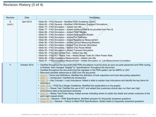
Revision Date Description
A June 2010 Initial release
B July 2010 Introduction: Enhanced definition of Vmin and Vmax. Explained that, beyond 25 MHz, the PDN is dominated by device
package internal RLC circuits.
PDN Theory: Added this section.
PCB Design Requirements: For frequency range 300 kHz–10 MHz, added the comment that each decoupling cap
must have its own via directly to the ground plane.
PDN Design Example: Clarified the reference design example as using the QSD8650A™ device. Added an important
note about the need for PMIC bulk caps.
Clarified the case 5 plots and added an explanation related to the increase/decrease of C/L.
FAQ: Rewritten, adding new FAQs. Added more information on simulation.
C August 2010 Clarified the following FAQs:
FAQ – PDN Guidelines; added figures and replaced the “fr” acronym with “ac”
FAQ – PDN Measurement Recommendations; added a figure
FAQ – Stress Test for Other Power Rails; reworded sentences
Added the following new FAQs:
FAQ – Mentor Graphics PADS Files
FAQ – Precautions for Layout Files
FAQ – PCB Stack-up
FAQ – Measuring PMIC DC Error
D September 2010 •Slide 6 – Added new slide, Scope and Intended Audience
•Slide 8 – Corrected typo in V(t) formula for F-1 in the Introduction
•Slide 14 – PDN Theory – updated figure for clarification
•Slide 18 – PCB Z(w) Design Guidelines – Removed the recommendation for 2x voltage rating on capacitor selection
•Slide 22:
•Added for PCB to PDN Maximum Impedance Guideline title
•Added new device MSM7x27T to PDN Maximum Impedance Guidelines
•Slide 25 – PDN Design Example – Added a note that all plots are simulations and correlate with actual measured
data
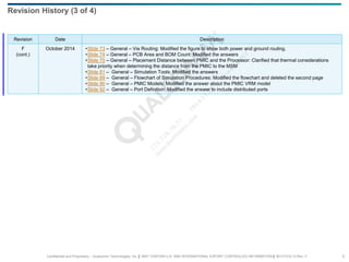
Revision History (1 of 4)
8.
Confidential and Proprietary– Qualcomm Technologies, Inc. | MAY CONTAIN U.S. AND INTERNATIONAL EXPORT CONTROLLED INFORMATION | 80-VT310-13 Rev. F 4
Revision Date Description
D
(cont.)
September 2010 •Slide 26 – PDN Design Example – Added a note about 10 mohm target PDN impedance guideline for DC
•Slide 39 – PDN Design Example, Modification 5, Step 3 – Labeled GND and power layers
•FAQ section:
•Slide 45 – FAQ – PDN Design Guidelines – Changed terminology Vpm to Vpmdcerror for consistency with other
slide and added scale in figure.
•Slide 50 – Files Needed for Simulation – Added a note about providing PCB stack-up information
•Slides 53 and 54 – Preparation for Layout File – Added examples
•Slide 63 – Distance and Heat Concentration – Added note about thermal conductivity
•Slides 67 and 68 – Via Routing – Updated figure for clarification
•Slide 75 – Measuring PMIC DC Error – Corrected formula in Vmargin_h, and removed rework for new configuration
requirement
•Added the following new FAQ:
•Slide 55 – Turn Around Time for Simulations
•Slides 56 and 57 – Flow Chart of the Simulation Environment
•Slide 78 – Overshoot Impact
•Slide 79 – Zero Ohm Resistor
E April 2012 •Slide 6 – Added AC1 and FAQ sub-sections to Agenda
•Slide 7 – Added Terms and Definitions
•Slide 17 – PDN Theory – Modified PDN circuit diagram
•Slide 25 – PDN Theory– Added Static IR Drop
•Slide 26 – PDN Theory – Added PCB Stack-up Considerations
•Slide 27 – PDN Theory – Added Capacitor Placements
•Slide 28 – PDN Theory – Added Decoupling Capacitor Routing Scenarios
•Slide 50 – AC1 Stress Test – Added title slide
•Slide 51 – AC1 Stress Test – Added Introduction and Recommended lab setup information
•Slide 52 – AC1 Stress Test – Added Probe Setup
•Slide 53 – AC1 Stress Test – Added Typical AC1 Waveform
•Slide 54 – AC1 Stress Test – Added Terms and Definitions
•Slide 55 – AC1 Stress Test – Added Terms and Definitions (cont.)
•Slide 56 – AC1 Stress Test – Added Margin Calculations
•Slide 57 – FAQ General – Added title slide
•Slide 58 – FAQ General – Added PDN Targets
Revision History (2 of 4)
9.
Confidential and Proprietary– Qualcomm Technologies, Inc. | MAY CONTAIN U.S. AND INTERNATIONAL EXPORT CONTROLLED INFORMATION | 80-VT310-13 Rev. F 5
Revision Date Description
E
(cont.)
April 2012 •Slide 60 – FAQ General – Modified PDN Guidelines (cont.)
•Slide 62 – FAQ General – Modified VRM Models, Transient Simulations
•Slide 73 – FAQ Simulation – Added new title
•Slide 77 – FAQ Simulation – Added additional files to be provided from Rev B.
•Slide 86 – FAQ Simulation – Added PMIC Models
•Slide 87 – FAQ Simulation – Added Package/Die Models
•Slide 88 – FAQ Simulation – Added Port Definition
•Slide 89 – FAQ Simulation – Added Resistance Measurement
•Slide 90 – FAQ Simulation – Added Current Measuring Resistor
•Slide 91 – FAQ Simulation – Added Time Domain Simulation
•Slide 92 – FAQ Simulation – Added Chip Power Model
•Slide 93 – FAQ Simulation – Added Transient Simulation
•Slide 94 – FAQ AC1 Stress Test – Added new title
•Slide 95 – FAQ AC1 Stress Test – Added Stress Tests for Other Power Rails
•Slide 96 – FAQ Impedance Measurement – Added new title
•Slide 97 – FAQ Impedance Measurement – Added Simulation vs. Lab Measurement Correlation
F October 2014 • Clarified throughout the document that PDN simulations must be done as soon as parts placement and PDN routing
is finished. Also changed “targets” to “specifications” throughout the document
• Clarified throughout the document that the regulator in the PDN system can be SMPS or LDO
• Removed obsolete references to QSD from the document
• Slide 8 – Terms and Definitions: Modified the definition of bulk capacitors and local decoupling capacitors
• Slide 11 – Introduction: Clarified the introduction
• Slide 19 – Key Concept – Loop Inductance: Added a slide to explain loop inductance and identify the key items for
reducing it
• Slide 23-26 – PCB Z(ω) Design Guidelines: Modified the explanations on the graphs
• Slide 53 – Stress Test: Clarified the use of AC1 and added that customers should also run their own high
concurrency tests at temperature extremes
• Slide 55 – Stress Test Probe Setup: Added arrows indicating where to solder the shield and center conductor of the
semi-rigid coaxial shield
• Slides 66 – General – PDN Specifications: Modified answers for frequently answered questions
• Slides 67-68 – General – Failure to Meet PDN Specifications: Added slides to frequently answered questions
Revision History (3 of 4)
10.
Confidential and Proprietary– Qualcomm Technologies, Inc. | MAY CONTAIN U.S. AND INTERNATIONAL EXPORT CONTROLLED INFORMATION | 80-VT310-13 Rev. F 6
Revision Date Description
F
(cont.)
October 2014 •Slide 73 – General – Via Routing: Modified the figure to show both power and ground routing.
•Slide 74 – General – PCB Area and BOM Count: Modified the answers
•Slide 75 – General – Placement Distance between PMIC and the Processor: Clarified that thermal considerations
take priority when determining the distance from the PMIC to the MSM
•Slide 81 – General – Simulation Tools: Modified the answers
•Slide 89 – General – Flowchart of Simulation Procedures: Modified the flowchart and deleted the second page
•Slide 90 – General – PMIC Models: Modified the answer about the PMIC VRM model
•Slide 92 – General – Port Definition: Modified the answer to include distributed ports
Revision History (3 of 4)
11.
Confidential and Proprietary– Qualcomm Technologies, Inc. | MAY CONTAIN U.S. AND INTERNATIONAL EXPORT CONTROLLED INFORMATION | 80-VT310-13 Rev. F 7
Contents
1 Introduction 9
2 PDN Theory 13
2.1 PCB Z(ω) Design Guidelines 22
3 PDN Design Example – Simulation 32
4 Stress Test (AC1) 52
5 Frequently Asked Questions 62
5.1 General 63
5.2 Simulation 79
12.
Confidential and Proprietary– Qualcomm Technologies, Inc. | MAY CONTAIN U.S. AND INTERNATIONAL EXPORT CONTROLLED INFORMATION | 80-VT310-13 Rev. F 8
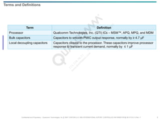
Terms and Definitions
Term Definition
Processor Qualcomm Technologies, Inc. (QTI) ICs – MSM™, APQ, MPQ, and MDM
Bulk capacitors Capacitors to smooth PMIC output response, normally by ≥ 4.7 µF
Local decoupling capacitors Capacitors closest to the processor. These capacitors improve processor
response to transient current demand, normally by ≤ 1 µF
13.
Confidential and Proprietary– Qualcomm Technologies, Inc. | MAY CONTAIN U.S. AND INTERNATIONAL EXPORT CONTROLLED INFORMATION | 80-VT310-13 Rev. F 9
Introduction
Section 1
14.
Confidential and Proprietary– Qualcomm Technologies, Inc. | MAY CONTAIN U.S. AND INTERNATIONAL EXPORT CONTROLLED INFORMATION | 80-VT310-13 Rev. F 10
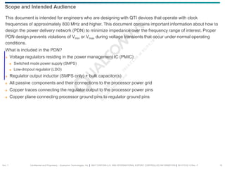
This document is intended for engineers who are designing with QTI devices that operate with clock
frequencies of approximately 800 MHz and higher. This document contains important information about how to
design the power delivery network (PDN) to minimize impedance over the frequency range of interest. Proper
PDN design prevents violations of Vmin or Vmax during voltage transients that occur under normal operating
conditions.
What is included in the PDN?
Voltage regulators residing in the power management IC (PMIC)
Switched mode power supply (SMPS)
Low-dropout regulator (LDO)
Regulator output inductor (SMPS only) + bulk capacitor(s)
All passive components and their connections to the processor power grid
Copper traces connecting the regulator output to the processor power pins
Copper plane connecting processor ground pins to regulator ground pins
Scope and Intended Audience
Sec. 1
15.
Confidential and Proprietary– Qualcomm Technologies, Inc. | MAY CONTAIN U.S. AND INTERNATIONAL EXPORT CONTROLLED INFORMATION | 80-VT310-13 Rev. F 11
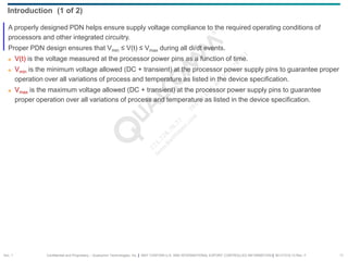
A properly designed PDN helps ensure supply voltage compliance to the required operating conditions of
processors and other integrated circuitry.
Proper PDN design ensures that Vmin ≤ V(t) ≤ Vmax during all di/dt events.
V(t) is the voltage measured at the processor power pins as a function of time.
Vmin is the minimum voltage allowed (DC + transient) at the processor power supply pins to guarantee proper
operation over all variations of process and temperature as listed in the device specification.
Vmax is the maximum voltage allowed (DC + transient) at the processor power supply pins to guarantee
proper operation over all variations of process and temperature as listed in the device specification.
Introduction (1 of 2)
Sec. 1
16.
Confidential and Proprietary– Qualcomm Technologies, Inc. | MAY CONTAIN U.S. AND INTERNATIONAL EXPORT CONTROLLED INFORMATION | 80-VT310-13 Rev. F 12
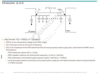
Key formula: V(t) = VDD(t) ± F-1{Z(ω)I(ω)}
VDD (t) is the instantaneous voltage at the PMIC output.
I(w) is the load current as a function of frequency.
Z(w) is the impedance of the PDN determined from the load (processor power supply pins), back toward the PMIC and is
dominated by:
– PCB metal power planes (DC to ~3 kHz)
– PMIC regulator response and external bulk capacitors (~3 kHz to ~300 kHz)
– PCB metal planes and local decoupling capacitor values (~300 kHz to ~10 MHz)
– Local decoupling capacitor connections to processor power supply pins and distance between power and ground planes
(~10 MHz onwards)
Introduction (2 of 2)
Sec. 1
17.
Confidential and Proprietary– Qualcomm Technologies, Inc. | MAY CONTAIN U.S. AND INTERNATIONAL EXPORT CONTROLLED INFORMATION | 80-VT310-13 Rev. F 13
PDN Theory
Section 2
2.1 PCB Z(ω) Design Guidelines 22
18.
Confidential and Proprietary– Qualcomm Technologies, Inc. | MAY CONTAIN U.S. AND INTERNATIONAL EXPORT CONTROLLED INFORMATION | 80-VT310-13 Rev. F 14
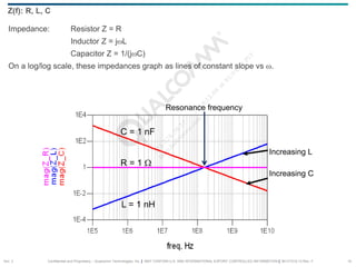
Impedance: Resistor Z = R
Inductor Z = jωL
Capacitor Z = 1/(jωC)
On a log/log scale, these impedances graph as lines of constant slope vs ω.
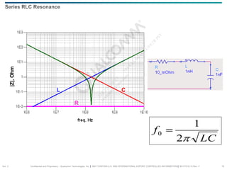
Z(f): R, L, C
R = 1 Ω
C = 1 nF
L = 1 nH
Increasing C
Increasing L
Resonance frequency
Sec. 2
19.
Confidential and Proprietary– Qualcomm Technologies, Inc. | MAY CONTAIN U.S. AND INTERNATIONAL EXPORT CONTROLLED INFORMATION | 80-VT310-13 Rev. F 15
Series RLC Resonance
LC
f
π
2
1
0 =
R
C
L
|Z|,
Ohm
Sec. 2
20.
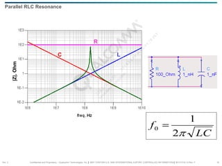
Confidential and Proprietary– Qualcomm Technologies, Inc. | MAY CONTAIN U.S. AND INTERNATIONAL EXPORT CONTROLLED INFORMATION | 80-VT310-13 Rev. F 16
Parallel RLC Resonance
LC
f
π
2
1
0 =
|Z|,
Ohm
R
L
C
Sec. 2
21.
Confidential and Proprietary– Qualcomm Technologies, Inc. | MAY CONTAIN U.S. AND INTERNATIONAL EXPORT CONTROLLED INFORMATION | 80-VT310-13 Rev. F 17
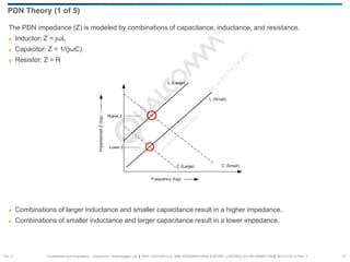
The PDN impedance (Z) is modeled by combinations of capacitance, inductance, and resistance.
Inductor: Z = jωL
Capacitor: Z = 1/(jωC)
Resistor: Z = R
Combinations of larger inductance and smaller capacitance result in a higher impedance.
Combinations of smaller inductance and larger capacitance result in a lower impedance.
PDN Theory (1 of 5)
Sec. 2
22.
Confidential and Proprietary– Qualcomm Technologies, Inc. | MAY CONTAIN U.S. AND INTERNATIONAL EXPORT CONTROLLED INFORMATION | 80-VT310-13 Rev. F 18
PDN Theory (2 of 5)
Note: This is a simplified PDN model.
Sec. 2
23.
Confidential and Proprietary– Qualcomm Technologies, Inc. | MAY CONTAIN U.S. AND INTERNATIONAL EXPORT CONTROLLED INFORMATION | 80-VT310-13 Rev. F 19
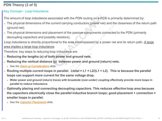
The amount of loop inductance associated with the PDN routing on a PCB is primarily determined by:
The physical dimensions of the current carrying conductors (power net) and the closeness of the return path
(ground net).
The physical dimensions and placement of the passive components connected to the PDN (primarily
decoupling capacitors and possibly resistors).
Loop inductance is directly proportional to the area encompassed by a power net and its return path. A large
area implies a large loop inductance.
Therefore, key steps to reducing loop inductance are:
Reducing the lengths (x) of both power and ground nets.
Reducing the vertical distance (y) between power and ground (return) nets.
See the Stack-up Considerations slide.
Routing multiple current loops in parallel. Ltotal = L1 × L2/(L1 + L2). This is because the parallel
loops can support more current for the same voltage drop.
Wider power and ground (return) traces with broadside (over-under) coupling effectively provide more loops in
parallel to reduce inductance.
Optimally placing and connecting decoupling capacitors. This reduces effective loop area because
the capacitors electrically close the parallel inductive branch loops; good placement + connection =
smaller loops in parallel.
See the Capacitor Placements slide.
Key Concept – Loop Inductance
PDN Theory (3 of 5)
Sec. 2
24.
Confidential and Proprietary– Qualcomm Technologies, Inc. | MAY CONTAIN U.S. AND INTERNATIONAL EXPORT CONTROLLED INFORMATION | 80-VT310-13 Rev. F 20
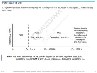
At higher frequencies (not shown in figure), the PDN impedance is a function of package RLC and board loop
inductance.
PDN Theory (4 of 5)
Note: The exact frequencies Fa, Fb, and Fc depend on the PMIC regulator used, bulk
capacitors, inductor (SMPS only), board impedance, decoupling capacitors, etc.
PCB
PMIC
+
Bulk capacitors
PCB
+
Decoupling capacitors
Connections to
local decoupling
capacitors,
their placement
relative to the
power pins,
and their values
0 Fa ~ 3 kHz Fb ~ 300 kHz Fc ~ 10 MHz
Impedance,
Z
(Ohm)
Sec. 2
25.
Confidential and Proprietary– Qualcomm Technologies, Inc. | MAY CONTAIN U.S. AND INTERNATIONAL EXPORT CONTROLLED INFORMATION | 80-VT310-13 Rev. F 21
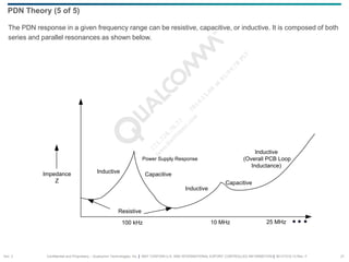
The PDN response in a given frequency range can be resistive, capacitive, or inductive. It is composed of both
series and parallel resonances as shown below.
PDN Theory (5 of 5)
Inductive Capacitive
10 MHz
Resistive
Impedance
Z Capacitive
Inductive
(Overall PCB Loop
Inductance)
Inductive
25 MHz
100 kHz
Power Supply Response
Sec. 2
26.
Confidential and Proprietary– Qualcomm Technologies, Inc. | MAY CONTAIN U.S. AND INTERNATIONAL EXPORT CONTROLLED INFORMATION | 80-VT310-13 Rev. F 22
PCB Z(ω) Design
Guidelines
Section 2.1
27.
Confidential and Proprietary– Qualcomm Technologies, Inc. | MAY CONTAIN U.S. AND INTERNATIONAL EXPORT CONTROLLED INFORMATION | 80-VT310-13 Rev. F 23
PCB
PMIC
+
Bulk capacitors
PCB
+
Decoupling capacitors
Connections to
local decoupling
capacitors,
their placement
relative to the
power pins,
and their values
0 Fa ~ 3 kHz
Impedance,
Z
(Ohm)
Fb ~ 300 kHz Fc ~ 10 MHz
DC–3 kHz → PCB metal routing to meet the DC resistance specification
First, address thermal design requirements relative to the placement of the PMIC and processor
Maximize metal thickness (½ vs. ⅓ oz. Cu)
Use sufficiently wide power traces
Use multiple parallel power and ground vias
PCB Z(ω) Design Guidelines (1 of 4)
Sec. 2.1
28.
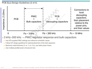
Confidential and Proprietary– Qualcomm Technologies, Inc. | MAY CONTAIN U.S. AND INTERNATIONAL EXPORT CONTROLLED INFORMATION | 80-VT310-13 Rev. F 24
PCB
PMIC
+
Bulk capacitors
PCB
+
Decoupling capacitors
Connections to
local
decoupling
capacitors,
their placement
relative to the
power pins,
and their values
0 Fa ~ 3 kHz
Impedance,
Z
(Ohm)
Fb ~ 300 kHz Fc ~ 10 MHz
3 kHz–300 kHz → PMIC regulator response and bulk capacitors
Use QTI-supplied PMIC settings and reference schematic values
Follow QTI design guidelines for optimal placement of the bulk capacitors
Maximize metal thickness (½ vs. ⅓ oz. Cu); use wider power traces
Use multiple parallel power and ground vias
PCB Z(ω) Design Guidelines (2 of 4)
Sec. 2.1
29.
Confidential and Proprietary– Qualcomm Technologies, Inc. | MAY CONTAIN U.S. AND INTERNATIONAL EXPORT CONTROLLED INFORMATION | 80-VT310-13 Rev. F 25
PCB
PMIC
+
Bulk capacitors
PCB
+
Decoupling capacitors
Connections to
local decoupling
capacitors,
their placement
relative to the
power pins,
and their values
0 Fa ~ 3 kHz
Impedance,
Z
(Ohm)
Fb ~ 300 kHz Fc ~ 10 MHz
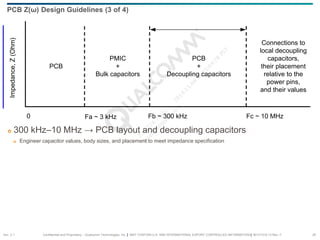
300 kHz–10 MHz → PCB layout and decoupling capacitors
Engineer capacitor values, body sizes, and placement to meet impedance specification
PCB Z(ω) Design Guidelines (3 of 4)
Sec. 2.1
30.
Confidential and Proprietary– Qualcomm Technologies, Inc. | MAY CONTAIN U.S. AND INTERNATIONAL EXPORT CONTROLLED INFORMATION | 80-VT310-13 Rev. F 26
PCB
PMIC
+
Bulk capacitors
PCB
+
Decoupling capacitors
Connections to
local
decoupling
capacitors,
their placement
relative to the
power pins,
and their values
0 Fa ~ 3 kHz
Impedance,
Z
(Ohm)
Fb ~ 300 kHz Fc ~ 10 MHz
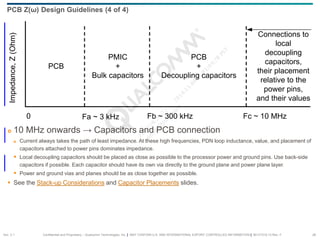
10 MHz onwards → Capacitors and PCB connection
Current always takes the path of least impedance. At these high frequencies, PDN loop inductance, value, and placement of
capacitors attached to power pins dominates impedance.
Local decoupling capacitors should be placed as close as possible to the processor power and ground pins. Use back-side
capacitors if possible. Each capacitor should have its own via directly to the ground plane and power plane layer.
Power and ground vias and planes should be as close together as possible.
See the Stack-up Considerations and Capacitor Placements slides.
PCB Z(ω) Design Guidelines (4 of 4)
Sec. 2.1
31.
Confidential and Proprietary– Qualcomm Technologies, Inc. | MAY CONTAIN U.S. AND INTERNATIONAL EXPORT CONTROLLED INFORMATION | 80-VT310-13 Rev. F 27
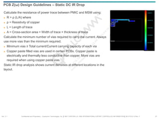
Calculate the resistance of power trace between PMIC and MSM using:
R = ρ (L/A) where
ρ = Resistivity of copper
L = Length of trace
A = Cross-section area = Width of trace × thickness of trace
Calculate the minimum number of vias required to carry the current. Always
use more vias than the minimum required.
Minimum vias ≥ Total current/Current carrying capacity of each via
Copper paste filled vias are used in certain PCBs. Copper paste is
electrically and thermally less conductive than copper. More vias are
required when using copper paste vias.
Static IR drop analysis shows current densities at different locations in the
layout.
PCB Z(ω) Design Guidelines – Static DC IR Drop
Sec. 2.1
32.
Confidential and Proprietary– Qualcomm Technologies, Inc. | MAY CONTAIN U.S. AND INTERNATIONAL EXPORT CONTROLLED INFORMATION | 80-VT310-13 Rev. F 28
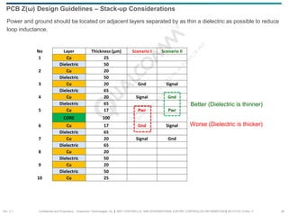
Power and ground should be located on adjacent layers separated by as thin a dielectric as possible to reduce
loop inductance.
PCB Z(ω) Design Guidelines – Stack-up Considerations
No Layer Thickness (μm) Scenario I Scenario II
1 Cu 25
Dielectric 50
2 Cu 20
Dielectric 50
3 Cu 20 Gnd Signal
Dielectric 65
4 Cu 20 Signal Gnd
Dielectric 65
5 Cu 17 Pwr Pwr
CORE 100
6 Cu 17 Gnd Signal
Dielectric 65
7 Cu 20 Signal Gnd
Dielectric 65
8 Cu 20
Dielectric 50
9 Cu 20
Dielectric 50
10 Cu 25
Better (Dielectric is thinner)
Worse (Dielectric is thicker)
Sec. 2.1
33.
Confidential and Proprietary– Qualcomm Technologies, Inc. | MAY CONTAIN U.S. AND INTERNATIONAL EXPORT CONTROLLED INFORMATION | 80-VT310-13 Rev. F 29
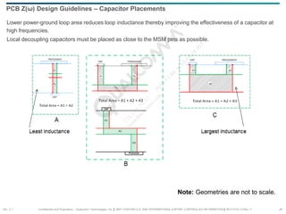
Lower power-ground loop area reduces loop inductance thereby improving the effectiveness of a capacitor at
high frequencies.
Local decoupling capacitors must be placed as close to the MSM pins as possible.
PCB Z(ω) Design Guidelines – Capacitor Placements
Note: Geometries are not to scale.
Sec. 2.1
34.
Confidential and Proprietary– Qualcomm Technologies, Inc. | MAY CONTAIN U.S. AND INTERNATIONAL EXPORT CONTROLLED INFORMATION | 80-VT310-13 Rev. F 30
Capacitor effective loop inductance is geometry based.
Body size influences self-inductance; capacitors with smaller body sizes have lower ESL.
Locate power-ground vias as close to each other as possible; small loops have lower inductance.
Locate vias close to the capacitor terminals; small loops have lower inductance.
Multiple parallel power-ground via pair connections reduce mounting inductance; parallel loops have lower
inductance.
Avoid sharing vias with adjacent capacitors; parallel loops have lower inductance, series loops have higher
inductance.
Three-terminal capacitors such as X2Y devices can offer lower inductance than two-terminal devices.
With good layout the three-terminal devices are connected with small loops and parallel loops.
The multiple terminal design also provides small loops and parallel loops inside the device for lower ESL.
PCB Z(ω) Design Guidelines – Decoupling Capacitor Routing
Sec. 2.1
35.
Confidential and Proprietary– Qualcomm Technologies, Inc. | MAY CONTAIN U.S. AND INTERNATIONAL EXPORT CONTROLLED INFORMATION | 80-VT310-13 Rev. F 31
PCB Z(ω) Design Guidelines – Decoupling Capacitors Response and Routing
Decreasing inductance
2-T Capacitors
3-T X2Y Capacitors
Good
Bad
Avoid sharing vias
Good Layout
Poor Layout
Poor Layout Good Layout
Typical Capacitor Response
Sec. 2.1
36.
Confidential and Proprietary– Qualcomm Technologies, Inc. | MAY CONTAIN U.S. AND INTERNATIONAL EXPORT CONTROLLED INFORMATION | 80-VT310-13 Rev. F 32
PDN Design Example –
Simulation
Section 3
Steps to Reduce the PDN Impedance of the PCB
37.
Confidential and Proprietary– Qualcomm Technologies, Inc. | MAY CONTAIN U.S. AND INTERNATIONAL EXPORT CONTROLLED INFORMATION | 80-VT310-13 Rev. F 33
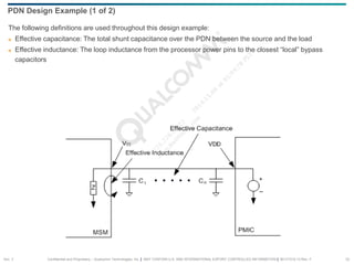
The following definitions are used throughout this design example:
Effective capacitance: The total shunt capacitance over the PDN between the source and the load
Effective inductance: The loop inductance from the processor power pins to the closest “local” bypass
capacitors
PDN Design Example (1 of 2)
Sec. 3
38.
Confidential and Proprietary– Qualcomm Technologies, Inc. | MAY CONTAIN U.S. AND INTERNATIONAL EXPORT CONTROLLED INFORMATION | 80-VT310-13 Rev. F 34
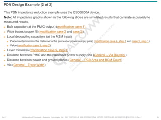
This PDN impedance reduction example uses the QSD8650A device.
Note: All impedance graphs shown in the following slides are simulated results that correlate accurately to
measured results.
Bulk capacitor (at the PMIC output) (modification case 1)
Wide traces/copper fill (modification case 2 and case 3)
Local decoupling capacitors (at the MSM input)
Placement (minimize the distance to the processor power supply pins) (modification case 4, step 1 and case 5, step 1)
Value (modification case 5, step 2)
Layer thickness (modification case 5, step 3)
Distance between PMIC and the processor power supply pins (General – Via Routing )
Distance between power and ground planes (General – PCB Area and BOM Count)
Via (General – Trace Width)
PDN Design Example (2 of 2)
Sec. 3
39.
Confidential and Proprietary– Qualcomm Technologies, Inc. | MAY CONTAIN U.S. AND INTERNATIONAL EXPORT CONTROLLED INFORMATION | 80-VT310-13 Rev. F 35
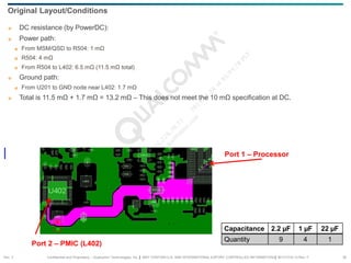
DC resistance (by PowerDC):
Power path:
From MSM/QSD to R504: 1 mΩ
R504: 4 mΩ
From R504 to L402: 6.5 mΩ (11.5 mΩ total)
Ground path:
From U201 to GND node near L402: 1.7 mΩ
Total is 11.5 mΩ + 1.7 mΩ = 13.2 mΩ – This does not meet the 10 mΩ specification at DC.
Original Layout/Conditions
Capacitance 2.2 µF 1 µF 22 µF
Quantity 9 4 1
Port 1 – Processor
Port 2 – PMIC (L402)
Sec. 3
40.
Confidential and Proprietary– Qualcomm Technologies, Inc. | MAY CONTAIN U.S. AND INTERNATIONAL EXPORT CONTROLLED INFORMATION | 80-VT310-13 Rev. F 36
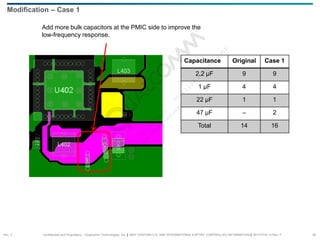
Modification – Case 1
Capacitance Original Case 1
2.2 µF 9 9
1 µF 4 4
22 µF 1 1
47 µF – 2
Total 14 16
Add more bulk capacitors at the PMIC side to improve the
low-frequency response.
Sec. 3
41.
Confidential and Proprietary– Qualcomm Technologies, Inc. | MAY CONTAIN U.S. AND INTERNATIONAL EXPORT CONTROLLED INFORMATION | 80-VT310-13 Rev. F 37
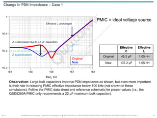
Change in PDN Impedance – Case 1
Effective
C
Effective
L
Original 45.3 µF 1.05 nH
New 137.2 µF 1.05 nH
Observation: Large bulk capacitors improve PDN impedance as shown, but even more important
is their role in reducing PMIC effective impedance below 100 kHz (not shown in these
simulations). Follow the PMIC data sheet and reference schematic for proper values (i.e., the
QSD8250A PMIC only recommends a 22 µF maximum bulk capacitor).
PMIC = ideal voltage source
1E5 1E6 1E7
1E4 1E8
1E-2
1E-1
1E-3
1
freq, Hz
Original
New
Z specification
Z is decreased due to 47 µF capacitors
Effective L unchanged
Sec. 3
42.
Confidential and Proprietary– Qualcomm Technologies, Inc. | MAY CONTAIN U.S. AND INTERNATIONAL EXPORT CONTROLLED INFORMATION | 80-VT310-13 Rev. F 38
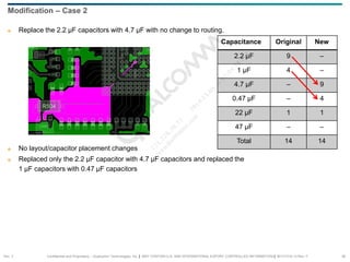
Replace the 2.2 µF capacitors with 4.7 µF with no change to routing.
No layout/capacitor placement changes
Replaced only the 2.2 µF capacitor with 4.7 µF capacitors and replaced the
1 µF capacitors with 0.47 µF capacitors
Modification – Case 2
Capacitance Original New
2.2 µF 9 –
1 µF 4 –
4.7 µF – 9
0.47 µF – 4
22 µF 1 1
47 µF – –
Total 14 14
Sec. 3
43.
Confidential and Proprietary– Qualcomm Technologies, Inc. | MAY CONTAIN U.S. AND INTERNATIONAL EXPORT CONTROLLED INFORMATION | 80-VT310-13 Rev. F 39
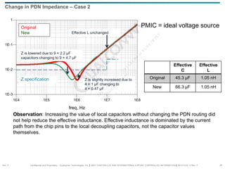
Change in PDN Impedance – Case 2
Effective
C
Effective
L
Original 45.3 µF 1.05 nH
New 66.3 µF 1.05 nH
Observation: Increasing the value of local capacitors without changing the PDN routing did
not help reduce the effective inductance. Effective inductance is dominated by the current
path from the chip pins to the local decoupling capacitors, not the capacitor values
themselves.
PMIC = ideal voltage source
1E5 1E6 1E7
1E4 1E8
1E-2
1E-1
1E-3
1
freq, Hz
Original
New
Z specification
Effective L unchanged
Z is lowered due to 9 × 2.2 µF
capacitors changing to 9 × 4.7 µF
Z is slightly increased due to
4 × 1 µF changing to
4 × 0.47 µF
Sec. 3
44.
Confidential and Proprietary– Qualcomm Technologies, Inc. | MAY CONTAIN U.S. AND INTERNATIONAL EXPORT CONTROLLED INFORMATION | 80-VT310-13 Rev. F 40
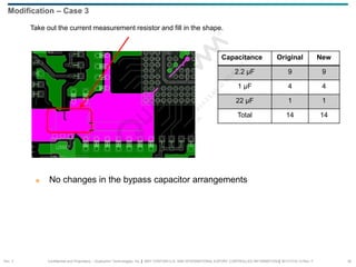
Modification – Case 3
Capacitance Original New
2.2 µF 9 9
1 µF 4 4
22 µF 1 1
Total 14 14
Take out the current measurement resistor and fill in the shape.
No changes in the bypass capacitor arrangements
Sec. 3
45.
Confidential and Proprietary– Qualcomm Technologies, Inc. | MAY CONTAIN U.S. AND INTERNATIONAL EXPORT CONTROLLED INFORMATION | 80-VT310-13 Rev. F 41
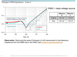
Change in PDN Impedance – Case 3
Effective
C
Effective
L
Original 45.3 µF 1.05 nH
New 45.3 µF 1.05 nH
PMIC = ideal voltage source
Observation: Removing the series R showed a 4 mΩ improvement in low-frequency
impedance from the MSM chip to the PMIC (see Original Layout/Conditions).
1E5 1E6 1E7
1E4 1E8
1E-2
1E-1
1E-3
1
freq, Hz
Original
New
Z specification
Small decrease in Z due to removal
of series resistance in the routing.
Sec. 3
46.
Confidential and Proprietary– Qualcomm Technologies, Inc. | MAY CONTAIN U.S. AND INTERNATIONAL EXPORT CONTROLLED INFORMATION | 80-VT310-13 Rev. F 42
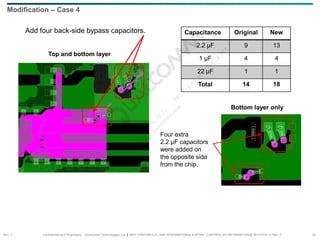
Modification – Case 4
Capacitance Original New
2.2 µF 9 13
1 µF 4 4
22 µF 1 1
Total 14 18
Add four back-side bypass capacitors.
Top and bottom layer
Bottom layer only
Four extra
2.2 µF capacitors
were added on
the opposite side
from the chip.
Sec. 3
47.
Confidential and Proprietary– Qualcomm Technologies, Inc. | MAY CONTAIN U.S. AND INTERNATIONAL EXPORT CONTROLLED INFORMATION | 80-VT310-13 Rev. F 43
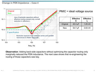
Change in PDN Impedance – Case 4
Effective
C
Effective
L
Original 45.3 µF 1.05 nH
New 54.7 µF 0.83 nH
Observation: Adding back-side capacitors without optimizing the capacitor routing only
marginally reduced the PDN inductance. The next case shows that re-engineering the
routing of those capacitors was key.
PMIC = ideal voltage source
1E5 1E6 1E7
1E4 1E8
1E-2
1E-1
1E-3
1
freq, Hz
Original
New
Z specification
Use of backside capacitors without
effective routing caused only a small
reduction in effective L.
Backside capacitor loop balances series and parallel
resonances to flatten response.
Sec. 3
48.
Confidential and Proprietary– Qualcomm Technologies, Inc. | MAY CONTAIN U.S. AND INTERNATIONAL EXPORT CONTROLLED INFORMATION | 80-VT310-13 Rev. F 44
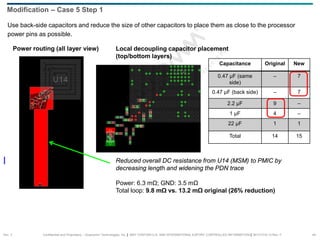
Use back-side capacitors and reduce the size of other capacitors to place them as close to the processor
power pins as possible.
Modification – Case 5 Step 1
Capacitance Original New
0.47 µF (same
side)
– 7
0.47 µF (back side) – 7
2.2 µF 9 –
1 µF 4 –
22 µF 1 1
Total 14 15
Power routing (all layer view) Local decoupling capacitor placement
(top/bottom layers)
Reduced overall DC resistance from U14 (MSM) to PMIC by
decreasing length and widening the PDN trace
Power: 6.3 mΩ; GND: 3.5 mΩ
Total loop: 9.8 mΩ vs. 13.2 mΩ original (26% reduction)
Sec. 3
49.
Confidential and Proprietary– Qualcomm Technologies, Inc. | MAY CONTAIN U.S. AND INTERNATIONAL EXPORT CONTROLLED INFORMATION | 80-VT310-13 Rev. F 45
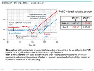
Change in PDN Impedance – Case 5 Step 1
Effective
C
Effective
L
Original 45.3 µF 1.05 nH
Step 1 29.0 µF 0.17 nH
PMIC = ideal voltage source
Observation: With an improved breakout strategy and re-engineering of the via patterns, the PDN
impedance is significantly reduced at both low and high frequency.
Back-side capacitors with close placement and short routing of the traces to the processor
power pins and ground plane reduce effective L. However, reduction of effective C has caused an
increase in impedance at mid frequency.
1E5 1E6 1E7
1E4 1E8
1E-2
1E-1
1E-3
1
freq, Hz
Original
New
Z specification
Properly routed backside
capacitors enable significant
decrease of effective L.
Z increases due to reduction of
effective C.
PMIC to MSM PDN shorter and
wider
Sec. 3