This document is a user manual for the LPC214x microcontrollers. It provides an overview of the microcontrollers' features, applications, device information, architectural overview, and memory maps. Key features include an ARM7 CPU, on-chip flash memory ranging from 32kB to 512kB, SRAM from 8kB to 40kB, and peripherals such as USB, ADC, DAC, timers, and GPIO. The manual is intended to help users understand and utilize the microcontrollers.

![UM10139
Philips Semiconductors
Volume 1
Chapter 1: Introductory information
• 60 MHz maximum CPU clock available from programmable on-chip PLL with settling
time of 100 µs.
• On-chip integrated oscillator operates with an external crystal in range from 1 MHz to
30 MHz and with an external oscillator up to 50 MHz.
• Power saving modes include Idle and Power-down.
• Individual enable/disable of peripheral functions as well as peripheral clock scaling for
additional power optimization.
• Processor wake-up from Power-down mode via external interrupt, USB, Brown-Out
Detect (BOD) or Real-Time Clock (RTC).
• Single power supply chip with Power-On Reset (POR) and BOD circuits:
– CPU operating voltage range of 3.0 V to 3.6 V (3.3 V ± 10 %) with 5 V tolerant I/O
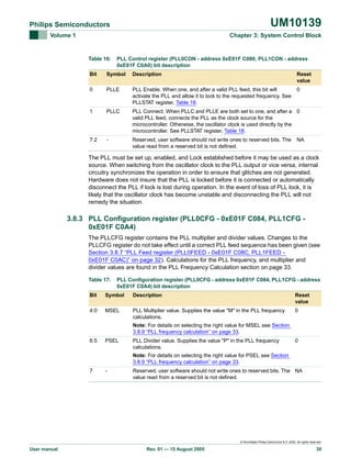
pads.
1.3 Applications
•
•
•
•
•
•
•
Industrial control
Medical systems
Access control
Point-of-sale
Communication gateway
Embedded soft modem
General purpose applications
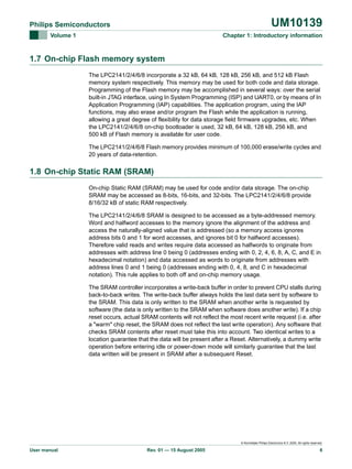
1.4 Device information
Table 1:
LPC2141/2/4/6/8 device information
Device
Number
of pins
On-chip
SRAM
Endpoint
USB RAM
On-chip
FLASH
Number of
10-bit ADC
channels
Number of
10-bit DAC
channels
Note
LPC2141
64
8 kB
2 kB
32 kB
6
-
-
LPC2142
64
16 kB
2 kB
64 kB
6
1
-
LPC2144
64
16 kB
2 kB
128 kB
14
1
UART1 with full modem
interface
LPC2146
64
32 kB + 8 kB[1] 2 kB
256 kB
14
1
UART1 with full modem
interface
LPC2148
64
32 kB + 8 kB[1] 2 kB
512 kB
14
1
UART1 with full modem
interface
[1]
While the USB DMA is the primary user of the additional 8 kB RAM, this RAM is also accessible at any time
by the CPU as a general purpose RAM for data and code storage.
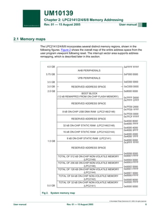
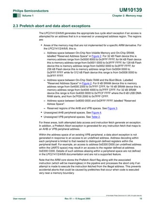
1.5 Architectural overview
The LPC2141/2/4/6/8 consists of an ARM7TDMI-S CPU with emulation support, the
ARM7 Local Bus for interface to on-chip memory controllers, the AMBA Advanced
High-performance Bus (AHB) for interface to the interrupt controller, and the VLSI
© Koninklijke Philips Electronics N.V. 2005. All rights reserved.
User manual
Rev. 01 — 15 August 2005
4](https://image.slidesharecdn.com/armusrmanl-131212220701-phpapp02/85/Arm-usr-m-anl-4-320.jpg)
![UM10139
Philips Semiconductors
Volume 1
Chapter 1: Introductory information
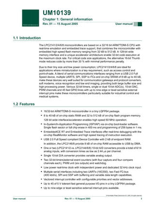
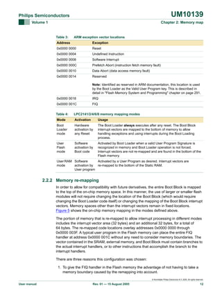
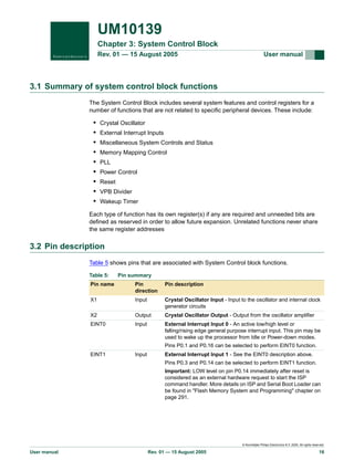
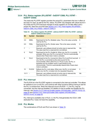
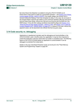
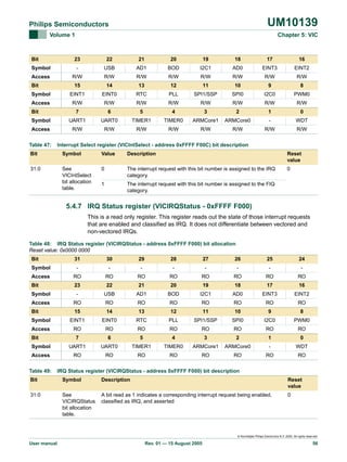
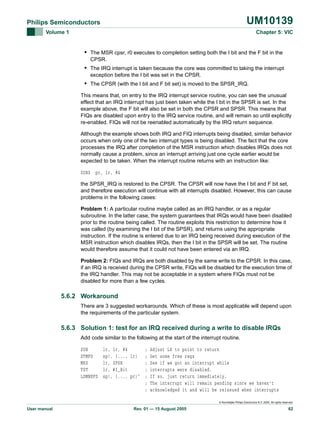
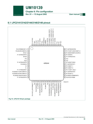
1.9 Block diagram
TMS(1)
TDI(1)
TRST(1)
TCK(1)
TDO(1)
P0[31:28] and
P0[25:0]
P1[31:16]
FAST GENERAL
PURPOSE I/O
EMULATION TRACE
MODULE
LPC2141/42/44/46/48
XTAL2
RST
XTAL1
TEST/DEBUG
INTERFACE
ARM7TDMI-S
AHB BRIDGE
PLL0
PLL1
USB
clock
ARM7 local bus
SYSTEM
FUNCTIONS
system
clock
VECTORED
INTERRUPT
CONTROLLER
AMBA AHB
(Advanced High-performance Bus)
INTERNAL
SRAM
CONTROLLER
INTERNAL
FLASH
CONTROLLER
8/16/32 kB
SRAM
32/64/128/256/512 kB
FLASH
AHB TO VPB
BRIDGE
VPB
DIVIDER
VPB (VLSI
peripheral bus)
AD0[7:6] and
AD0[4:1]
AD1[7:0](2)
AHB
DECODER
EXTERNAL
INTERRUPTS
CAPTURE/COMPARE
(W/EXTERNAL CLOCK)
TIMER 0/TIMER 1
I2C-BUS SERIAL
INTERFACES 0 AND 1
A/D CONVERTERS
0 AND 1(2)
D+
D−
UP_LED
CONNECT
VBUS
USB 2.0 FULL-SPEED
DEVICE CONTROLLER
WITH DMA(3)
SPI AND SSP
SERIAL INTERFACES
EINT3 to EINT0
4 × CAP0
4 × CAP1
8 × MAT0
8 × MAT1
8 kB RAM
SHARED WITH
USB DMA(3)
SCL0, SCL1
SDA0, SDA1
SCK0, SCK1
MOSI0, MOSI1
MISO0, MISO1
SSEL0, SSEL1
TXD0, TXD1
AOUT(4)
D/A CONVERTER
GENERAL
PURPOSE I/O
REAL-TIME CLOCK
PWM0
RXD0, RXD1
UART0/UART1
WATCHDOG
TIMER
P0[31:28] and
P0[25:0]
P1[31:16]
PWM6 to PWM0
DSR1(2),CTS1(2),
RTS1(2), DTR1(2)
DCD1(2),RI1(2)
RTXC1
RTXC2
VBAT
SYSTEM
CONTROL
002aab560
(1) Pins shared with GPIO.
(2) LPCC2144/6/8 only.
(3) USB DMA controller with 8 kB of RAM accessible as general purpose RAM and/or DMA is available in LPC2146/8 only.
(4) LPC2142/4/6/8 only.
Fig 1. LPC2141/2/4/6/8 block diagram
© Koninklijke Philips Electronics N.V. 2005. All rights reserved.
User manual
Rev. 01 — 15 August 2005
7](https://image.slidesharecdn.com/armusrmanl-131212220701-phpapp02/85/Arm-usr-m-anl-7-320.jpg)
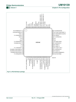
![UM10139
Philips Semiconductors
Volume 1
Chapter 3: System Control Block
Table 5:
Pin summary
Pin name
Pin
direction
Pin description
EINT2
Input
External Interrupt Input 2 - See the EINT0 description above.
Pins P0.7 and P0.15 can be selected to perform EINT2 function.
EINT3
Input
External Interrupt Input 3 - See the EINT0 description above.
Pins P0.9, P0.20 and P0.30 can be selected to perform EINT3
function.
RESET
Input
External Reset input - A LOW on this pin resets the chip, causing
I/O ports and peripherals to take on their default states, and the
processor to begin execution at address 0x0000 0000.
3.3 Register description
All registers, regardless of size, are on word address boundaries. Details of the registers
appear in the description of each function.
Table 6:
Summary of system control registers
Name
Description
Access
Reset
value[1]
Address
External Interrupts
EXTINT
External Interrupt Flag Register
R/W
0
0xE01F C140
INTWAKE
Interrupt Wakeup Register
R/W
0
0xE01F C144
EXTMODE
External Interrupt Mode Register
R/W
0
0xE01F C148
EXTPOLAR
External Interrupt Polarity Register
R/W
0
0xE01F C14C
R/W
0
0xE01F C040
Memory Mapping Control
MEMMAP
Memory Mapping Control
Phase Locked Loop
PLL0CON
PLL0 Control Register
R/W
0
0xE01F C080
PLL0CFG
PLL0 Configuration Register
R/W
0
0xE01F C084
PLL0STAT
PLL0 Status Register
RO
0
0xE01F C088
PLL0FEED
PLL0 Feed Register
WO
NA
0xE01F C08C
PLL1CON
PLL1 (USB) Control Register
R/W
0
0xE01F C0A0
PLL1CFG
PLL1 (USB) Configuration Register
R/W
0
0xE01F C0A4
PLL1STAT
PLL1 (USB) Status Register
RO
0
0xE01F C0A8
PLL1FEED
PLL1 (USB) Feed Register
WO
NA
0xE01F C0AC
PCON
Power Control Register
R/W
0
0xE01F C0C0
PCONP
Power Control for Peripherals
R/W
0x03BE
0xE01F C0C4
VPB Divider Control
R/W
0
0xE01F C100
Reset Source Identification Register
R/W
0
0xE01F C180
Power Control
VPB Divider
VPBDIV
Reset
RSID
Code Security/Debugging
© Koninklijke Philips Electronics N.V. 2005. All rights reserved.
User manual
Rev. 01 — 15 August 2005
17](https://image.slidesharecdn.com/armusrmanl-131212220701-phpapp02/85/Arm-usr-m-anl-17-320.jpg)
![UM10139
Philips Semiconductors
Volume 1
Chapter 3: System Control Block
Table 6:
Summary of system control registers
Name
Description
Access
Reset
value[1]
Address
CSPR
Code Security Protection Register
RO
0
0xE01F C184
R/W
0
0xE01F C1A0
Syscon Miscellaneous Registers
SCS
[1]
System Controls and Status
Reset value reflects the data stored in used bits only. It does not include reserved bits content.
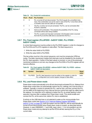
3.4 Crystal oscillator
While an input signal of 50-50 duty cycle within a frequency range from 1 MHz to 50 MHz
can be used by the LPC2141/2/4/6/8 if supplied to its input XTAL1 pin, this
microcontroller’s onboard oscillator circuit supports external crystals in the range of 1 MHz
to 30 MHz only. If the on-chip PLL system or the boot-loader is used, the input clock
frequency is limited to an exclusive range of 10 MHz to 25 MHz.
The oscillator output frequency is called FOSC and the ARM processor clock frequency is
referred to as CCLK for purposes of rate equations, etc. elsewhere in this document. FOSC
and CCLK are the same value unless the PLL is running and connected. Refer to the
Section 3.8 “Phase Locked Loop (PLL)” on page 27 for details and frequency limitations.
The onboard oscillator in the LPC2141/2/4/6/8 can operate in one of two modes: slave
mode and oscillation mode.
In slave mode the input clock signal should be coupled by means of a capacitor of 100 pF
(CC in Figure 6, drawing a), with an amplitude of at least 200 mVrms. The X2 pin in this
configuration can be left not connected. If slave mode is selected, the FOSC signal of 50-50
duty cycle can range from 1 MHz to 50 MHz.
External components and models used in oscillation mode are shown in Figure 6,
drawings b and c, and in Table 7. Since the feedback resistance is integrated on chip, only
a crystal and the capacitances CX1 and CX2 need to be connected externally in case of
fundamental mode oscillation (the fundamental frequency is represented by L, CL and
RS). Capacitance CP in Figure 6, drawing c, represents the parallel package capacitance
and should not be larger than 7 pF. Parameters FC, CL, RS and CP are supplied by the
crystal manufacturer.
Choosing an oscillation mode as an on-board oscillator mode of operation limits FOSC
clock selection to 1 MHz to 30 MHz.
© Koninklijke Philips Electronics N.V. 2005. All rights reserved.
User manual
Rev. 01 — 15 August 2005
18](https://image.slidesharecdn.com/armusrmanl-131212220701-phpapp02/85/Arm-usr-m-anl-18-320.jpg)
![UM10139
Philips Semiconductors
Volume 1
Chapter 3: System Control Block
f OSC selection
True
On-chip PLL used
in application?
False
True
ISP used for initial
code download?
False
External crystal
oscillator used?
True
False
MIN f
= 10 MHz
OSC
MAX f OSC = 25 MHz
MIN fOSC = 1 MHz
MAX f OSC = 50 MHz
MIN fOSC = 1 MHz
MAX f OSC = 30 MHz
(Figure 7, mode a and/or b)
(Figure 7, mode a)
(Figure 7, mode b)
Fig 7. FOSC selection algorithm
3.5 External interrupt inputs
The LPC2141/2/4/6/8 includes four External Interrupt Inputs as selectable pin functions.
The External Interrupt Inputs can optionally be used to wake up the processor from
Power-down mode.
3.5.1 Register description
The external interrupt function has four registers associated with it. The EXTINT register
contains the interrupt flags, and the EXTWAKEUP register contains bits that enable
individual external interrupts to wake up the microcontroller from Power-down mode. The
EXTMODE and EXTPOLAR registers specify the level and edge sensitivity parameters.
Table 8:
External interrupt registers
Name
Description
Access Reset
Address
value[1]
EXTINT
The External Interrupt Flag Register contains
interrupt flags for EINT0, EINT1, EINT2 and
EINT3. See Table 9.
R/W
0
0xE01F C140
© Koninklijke Philips Electronics N.V. 2005. All rights reserved.
User manual
Rev. 01 — 15 August 2005
20](https://image.slidesharecdn.com/armusrmanl-131212220701-phpapp02/85/Arm-usr-m-anl-20-320.jpg)
![UM10139
Philips Semiconductors
Volume 1
Chapter 3: System Control Block
Table 8:
External interrupt registers
Name
Description
Access Reset
Address
value[1]
INTWAKE
The Interrupt Wakeup Register contains four
enable bits that control whether each external
interrupt will cause the processor to wake up
from Power-down mode. See Table 10.
R/W
0
0xE01F C144
EXTMODE
The External Interrupt Mode Register controls
whether each pin is edge- or level sensitive.
R/W
0
0xE01F C148
EXTPOLAR
The External Interrupt Polarity Register controls R/W
which level or edge on each pin will cause an
interrupt.
0
0xE01F C14C
[1]
Reset value reflects the data stored in used bits only. It does not include reserved bits content.
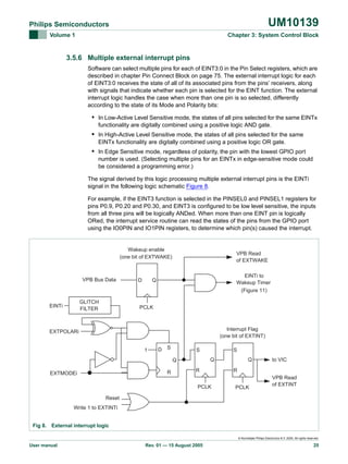
3.5.2 External Interrupt Flag register (EXTINT - 0xE01F C140)
When a pin is selected for its external interrupt function, the level or edge on that pin
(selected by its bits in the EXTPOLAR and EXTMODE registers) will set its interrupt flag in
this register. This asserts the corresponding interrupt request to the VIC, which will cause
an interrupt if interrupts from the pin are enabled.
Writing ones to bits EINT0 through EINT3 in EXTINT register clears the corresponding
bits. In level-sensitive mode this action is efficacious only when the pin is in its inactive
state.
Once a bit from EINT0 to EINT3 is set and an appropriate code starts to execute (handling
wakeup and/or external interrupt), this bit in EXTINT register must be cleared. Otherwise
the event that was just triggered by activity on the EINT pin will not be recognized in the
future.
Important: whenever a change of external interrupt operating mode (i.e. active
level/edge) is performed (including the initialization of an external interrupt), the
corresponding bit in the EXTINT register must be cleared! For details see Section
3.5.4 “External Interrupt Mode register (EXTMODE - 0xE01F C148)” and Section 3.5.5
“External Interrupt Polarity register (EXTPOLAR - 0xE01F C14C)”.
For example, if a system wakes up from power-down using a low level on external
interrupt 0 pin, its post-wakeup code must reset the EINT0 bit in order to allow future entry
into the power-down mode. If the EINT0 bit is left set to 1, subsequent attempt(s) to invoke
power-down mode will fail. The same goes for external interrupt handling.
More details on power-down mode will be discussed in the following chapters.
© Koninklijke Philips Electronics N.V. 2005. All rights reserved.
User manual
Rev. 01 — 15 August 2005
21](https://image.slidesharecdn.com/armusrmanl-131212220701-phpapp02/85/Arm-usr-m-anl-21-320.jpg)
![UM10139
Philips Semiconductors
Volume 1
Chapter 3: System Control Block
Table 14:
Memory Mapping control register (MEMMAP - address 0xE01F C040) bit
description
Bit
Symbol Value
Description
Reset
value
1:0
MAP
00
Boot Loader Mode. Interrupt vectors are re-mapped to Boot
Block.
00
01
User Flash Mode. Interrupt vectors are not re-mapped and
reside in Flash.
10
User RAM Mode. Interrupt vectors are re-mapped to Static
RAM.
11
Reserved. Do not use this option.
Warning: Improper setting of this value may result in incorrect
operation of the device.
7:2
-
-
Reserved, user software should not write ones to reserved
bits. The value read from a reserved bit is not defined.
NA
3.7.2 Memory mapping control usage notes
The Memory Mapping Control simply selects one out of three available sources of data
(sets of 64 bytes each) necessary for handling ARM exceptions (interrupts).
For example, whenever a Software Interrupt request is generated, the ARM core will
always fetch 32-bit data "residing" on 0x0000 0008 see Table 3 “ARM exception vector
locations” on page 12. This means that when MEMMAP[1:0]=10 (User RAM Mode), a
read/fetch from 0x0000 0008 will provide data stored in 0x4000 0008. In case of
MEMMAP[1:0]=00 (Boot Loader Mode), a read/fetch from 0x0000 0008 will provide data
available also at 0x7FFF E008 (Boot Block remapped from on-chip Bootloader).
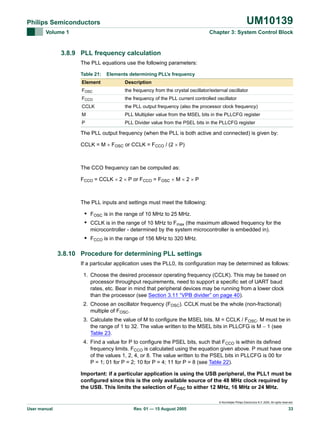
3.8 Phase Locked Loop (PLL)
There are two PLL modules in the LPC2141/2/4/6/8 microcontroller. The PLL0 is used to
generate the CCLK clock (system clock) while the PLL1 has to supply the clock for the
USB at the fixed rate of 48 MHz. Structurally these two PLLs are identical with exception
of the PLL interrupt capabilities reserved only for the PLL0.
The PLL0 and PLL1 accept an input clock frequency in the range of 10 MHz to 25 MHz
only. The input frequency is multiplied up the range of 10 MHz to 60 MHz for the CCLK
and 48 MHz for the USB clock using a Current Controlled Oscillators (CCO). The
multiplier can be an integer value from 1 to 32 (in practice, the multiplier value cannot be
higher than 6 on the LPC2141/2/4/6/8 due to the upper frequency limit of the CPU). The
CCO operates in the range of 156 MHz to 320 MHz, so there is an additional divider in the
loop to keep the CCO within its frequency range while the PLL is providing the desired
output frequency. The output divider may be set to divide by 2, 4, 8, or 16 to produce the
output clock. Since the minimum output divider value is 2, it is insured that the PLL output
has a 50% duty cycle. A block diagram of the PLL is shown in Figure 9.
PLL activation is controlled via the PLLCON register. The PLL multiplier and divider values
are controlled by the PLLCFG register. These two registers are protected in order to
prevent accidental alteration of PLL parameters or deactivation of the PLL. Since all chip
operations, including the Watchdog Timer, are dependent on the PLL0 when it is providing
the chip clock, accidental changes to the PLL setup could result in unexpected behavior of
© Koninklijke Philips Electronics N.V. 2005. All rights reserved.
User manual
Rev. 01 — 15 August 2005
27](https://image.slidesharecdn.com/armusrmanl-131212220701-phpapp02/85/Arm-usr-m-anl-27-320.jpg)
![UM10139
Philips Semiconductors
Volume 1
Chapter 3: System Control Block
the microcontroller. The same concern is present with the PLL1 and the USB. The
protection is accomplished by a feed sequence similar to that of the Watchdog Timer.
Details are provided in the description of the PLLFEED register.
Both PLLs are turned off and bypassed following a chip Reset and when by entering
Power-down mode. The PLL is enabled by software only. The program must configure and
activate the PLL, wait for the PLL to Lock, then connect to the PLL as a clock source.
3.8.1 Register description
The PLL is controlled by the registers shown in Table 15. More detailed descriptions
follow.
Warning: Improper setting of the PLL0 and PLL1 values may result in incorrect
operation of the device and the USB module!
Table 15:
PLL registers
Generic
name
Description
Access Reset
System clock
value[1] (PLL0)
Address & Name
USB 48 MHz
clock (PLL1)
Address & Name
PLLCON
PLL Control Register. Holding register for
updating PLL control bits. Values written to this
register do not take effect until a valid PLL feed
sequence has taken place.
R/W
0
0xE01F C080
PLL0CON
0xE01F C0A0
PLL1CON
PLLCFG
PLL Configuration Register. Holding register for
updating PLL configuration values. Values
written to this register do not take effect until a
valid PLL feed sequence has taken place.
R/W
0
0xE01F C084
PLL0CFG
0xE01F C0A4
PLL1CFG
PLLSTAT
PLL Status Register. Read-back register for PLL RO
control and configuration information. If
PLLCON or PLLCFG have been written to, but a
PLL feed sequence has not yet occurred, they
will not reflect the current PLL state. Reading
this register provides the actual values
controlling the PLL, as well as the status of the
PLL.
0
0xE01F C088
PLL0STAT
0xE01F C0A8
PLL1STAT
PLLFEED
PLL Feed Register. This register enables
loading of the PLL control and configuration
information from the PLLCON and PLLCFG
registers into the shadow registers that actually
affect PLL operation.
NA
0xE01F C08C
PLL0FEED
0xE01F C0AC
PLL1FEED
[1]
WO
Reset value reflects the data stored in used bits only. It does not include reserved bits content.
© Koninklijke Philips Electronics N.V. 2005. All rights reserved.
User manual
Rev. 01 — 15 August 2005
28](https://image.slidesharecdn.com/armusrmanl-131212220701-phpapp02/85/Arm-usr-m-anl-28-320.jpg)
![UM10139
Philips Semiconductors
Volume 1
Chapter 3: System Control Block
PLLC
CLOCK
SYNCHRONIZATION
0
Direct
PSEL[1:0]
PD
PD
PLLE
0
Bypass
F OSC
1
PHASEFREQUENCY
DETECTOR
PLOCK
CCO
F CCO
CD
0
/2P
0
0
CCLK
1
1
PD
F OUT
CD
DIV-BY-M
MSEL<4:0>
MSEL[4:0]
Fig 9. PLL block diagram
3.8.2 PLL Control register (PLL0CON - 0xE01F C080, PLL1CON 0xE01F C0A0)
The PLLCON register contains the bits that enable and connect the PLL. Enabling the
PLL allows it to attempt to lock to the current settings of the multiplier and divider values.
Connecting the PLL causes the processor and all chip functions to run from the PLL
output clock. Changes to the PLLCON register do not take effect until a correct PLL feed
sequence has been given (see Section 3.8.7 “PLL Feed register (PLL0FEED 0xE01F C08C, PLL1FEED - 0xE01F C0AC)” and Section 3.8.3 “PLL Configuration
register (PLL0CFG - 0xE01F C084, PLL1CFG - 0xE01F C0A4)” on page 30).
© Koninklijke Philips Electronics N.V. 2005. All rights reserved.
User manual
Rev. 01 — 15 August 2005
29](https://image.slidesharecdn.com/armusrmanl-131212220701-phpapp02/85/Arm-usr-m-anl-29-320.jpg)
![UM10139
Philips Semiconductors
Volume 1
Chapter 3: System Control Block
Table 22:
PLL Divider values
PSEL Bits (PLLCFG bits [6:5])
Value of P
00
1
01
2
10
4
11
8
Table 23:
PLL Multiplier values
MSEL Bits (PLLCFG bits [4:0])
Value of M
00000
1
00001
2
00010
3
00011
4
...
...
11110
31
11111
32
3.8.11 PLL0 and PLL1 configuring examples
Example 1: an application not using the USB - configuring the PLL0
System design asks for FOSC= 10 MHz and requires CCLK = 60 MHz.
Based on these specifications, M = CCLK / Fosc = 60 MHz / 10 MHz = 6. Consequently,
M - 1 = 5 will be written as PLLCFG[4:0].
Value for P can be derived from P = FCCO / (CCLK x 2), using condition that FCCO must be
in range of 156 MHz to 320 MHz. Assuming the lowest allowed frequency for
FCCO = 156 MHz, P = 156 MHz / (2 x 60 MHz) = 1.3. The highest FCCO frequency criteria
produces P = 2.67. The only solution for P that satisfies both of these requirements and is
listed in Table 22 is P = 2. Therefore, PLLCFG[6:5] = 1 will be used.
Example 2: an application using the USB - configuring the PLL1
System design asks for FOSC= 12 MHz and requires the USB clock of 48 MHz.
Based on these specifications, M = 48 MHz / Fosc = 48 MHz / 12 MHz = 4. Consequently,
M - 1 = 3 will be written as PLLCFG[4:0].
Value for P can be derived from P = FCCO / (48 MHz x 2), using condition that FCCO must
be in range of 156 MHz to 320 MHz. Assuming the lowest allowed frequency for
FCCO = 156 MHz, P = 156 MHz / (2 x 48 MHz) = 1.625. The highest FCCO frequency
criteria produces P = 3.33. Solution for P that satisfy both of these requirements and are
listed in Table 22 are P = 2 and P = 3. Therefore, either of these two values can be used to
program PLLCFG[6:5] in the PLL1.
Example 2 has illustrated the way PLL1 should be configured. Since PLL0 and PLL1 are
independent, the PLL0 can be configured using the approach described in Example 1.
© Koninklijke Philips Electronics N.V. 2005. All rights reserved.
User manual
Rev. 01 — 15 August 2005
34](https://image.slidesharecdn.com/armusrmanl-131212220701-phpapp02/85/Arm-usr-m-anl-34-320.jpg)
![UM10139
Philips Semiconductors
Volume 1
Chapter 3: System Control Block
3.9 Power control
The LPC2141/2/4/6/8 supports two reduced power modes: Idle mode and Power-down
mode. In Idle mode, execution of instructions is suspended until either a Reset or interrupt
occurs. Peripheral functions continue operation during Idle mode and may generate
interrupts to cause the processor to resume execution. Idle mode eliminates power used
by the processor itself, memory systems and related controllers, and internal buses.
In Power-down mode, the oscillator is shut down and the chip receives no internal clocks.
The processor state and registers, peripheral registers, and internal SRAM values are
preserved throughout Power-down mode and the logic levels of chip pins remain static.
The Power-down mode can be terminated and normal operation resumed by either a
Reset or certain specific interrupts that are able to function without clocks. Since all
dynamic operation of the chip is suspended, Power-down mode reduces chip power
consumption to nearly zero.
Entry to Power-down and Idle modes must be coordinated with program execution.
Wakeup from Power-down or Idle modes via an interrupt resumes program execution in
such a way that no instructions are lost, incomplete, or repeated. Wake up from
Power-down mode is discussed further in Section 3.12 “Wakeup timer” on page 41.
A Power Control for Peripherals feature allows individual peripherals to be turned off if
they are not needed in the application, resulting in additional power savings.
3.9.1 Register description
The Power Control function contains two registers, as shown in Table 24. More detailed
descriptions follow.
Table 24:
Power control registers
Name
Description
Access Reset
value[1]
PCON
Power Control Register. This register contains R/W
control bits that enable the two reduced power
operating modes of the microcontroller. See
Table 25.
0x00
PCONP Power Control for Peripherals Register. This
R/W
register contains control bits that enable and
disable individual peripheral functions,
Allowing elimination of power consumption by
peripherals that are not needed.
[1]
Address
0xE01F C0C0
0x0018 17BE 0xE01F C0C4
Reset value reflects the data stored in used bits only. It does not include reserved bits content.
3.9.2 Power Control register (PCON - 0xE01F COCO)
The PCON register contains two bits. Writing a one to the corresponding bit causes entry
to either the Power-down or Idle mode. If both bits are set, Power-down mode is entered.
© Koninklijke Philips Electronics N.V. 2005. All rights reserved.
User manual
Rev. 01 — 15 August 2005
35](https://image.slidesharecdn.com/armusrmanl-131212220701-phpapp02/85/Arm-usr-m-anl-35-320.jpg)
![UM10139
Philips Semiconductors
Volume 1
Chapter 3: System Control Block
Table 25:
Power Control register (PCON - address 0xE01F COCO) bit description
Bit
Symbol
Description
Reset
value
0
IDL
Idle mode - when 1, this bit causes the processor clock to be stopped,
while on-chip peripherals remain active. Any enabled interrupt from a
peripheral or an external interrupt source will cause the processor to
resume execution.
0
1
PD
Power-down mode - when 1, this bit causes the oscillator and all
on-chip clocks to be stopped. A wakeup condition from an external
interrupt can cause the oscillator to restart, the PD bit to be cleared,
and the processor to resume execution.
0
IMPORTANT: PD bit can be set to 1 at any time if USBWAKE = 0. In
case of USBWAKE = 1, it is possible to set PD to 1 only if
USB_need_clock = 0. Having both USBWAKE and
USB_need_clock equal 1 prevents the microcontroller from
entering Power-down mode. (For additional details see Section 3.5.3
“Interrupt Wakeup register (INTWAKE - 0xE01F C144)” on page 22 and
Section 14.7.1 “USB Interrupt Status register (USBIntSt 0xE01F C1C0)” on page 200)
2
PDBOD
3
BODPDM When this bit is 1, the BOD circuitry will go into power down mode when 0
chip power down is asserted, resulting in a further reduction in power.
However, the possibility of using BOD as a wakeup source from Power
Down mode will be lost. When this bit is 0, BOD stays active during
Power Down mode.
4
BOGD
Brown Out Global Disable. When this bit is 1, the BOD circuitry is fully
disabled at all times, and will not consume power. When 0, the BOD
circuitry is enabled.
0
5
BORD
Brown Out Reset Disable. When this bit is 1, the second stage of low
voltage detection (2.6 V) will not cause a chip reset. When BORD is 0,
the reset is enabled. The first stage of low voltage detection (2.9 V)
Brown Out interrupt is not affected.
0
7:6
-
Reserved, user software should not write ones to reserved bits. The
value read from a reserved bit is not defined.
NA
[1]
When PD is 1 and this bit is 0, Brown Out Detection (BOD) remains
0
operative during Power-down mode, such that its Reset can release the
microcontroller from Power-down mode[1]. When PD and this bit are
both 1, the BOD circuit is disabled during Power-down mode to
conserve power. When PD is 0, the state of this bit has no effect.
Since execution is delayed until after the Wakeup Timer has allowed the main oscillator to resume stable
operation, there is no guarantee that execution will resume before VDD has fallen below the lower BOD
threshold, which prevents execution. If execution does resume, there is no guarantee of how long the
microcontroller will continue execution before the lower BOD threshold terminates execution. These issues
depend on the slope of the decline of VDD. High decoupling capacitance (between VDD and ground) in the
vicinity of the microcontroller will improve the likelihood that software will be able to do what needs to be
done when power is being lost.
3.9.3 Power Control for Peripherals register (PCONP - 0xE01F COC4)
The PCONP register allows turning off selected peripheral functions for the purpose of
saving power. This is accomplished by gating off the clock source to the specified
peripheral blocks. A few peripheral functions cannot be turned off (i.e. the Watchdog timer,
GPIO, the Pin Connect block, and the System Control block). Some peripherals,
particularly those that include analog functions, may consume power that is not clock
dependent. These peripherals may contain a separate disable control that turns off
© Koninklijke Philips Electronics N.V. 2005. All rights reserved.
User manual
Rev. 01 — 15 August 2005
36](https://image.slidesharecdn.com/armusrmanl-131212220701-phpapp02/85/Arm-usr-m-anl-36-320.jpg)
![UM10139
Philips Semiconductors
Volume 1
Chapter 3: System Control Block
Table 27:
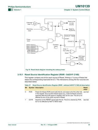
Reset Source identification Register (RSIR - address 0xE01F C180) bit description
Bit
Symbol Description
Reset
value
2
WDTR
This bit is set when the Watchdog Timer times out and the WDTRESET see text
bit in the Watchdog Mode Register is 1. It is cleared by any of the other
sources of Reset.
3
BODR
This bit is set when the 3.3 V power reaches a level below 2.6 V. If the
see text
VDD voltage dips from 3.3 V to 2.5 V and backs up, the BODR bit will be
set to 1. Also, if the VDD voltage rises continuously from below 1 V to a
level above 2.6 V, the BODR will be set to 1, too. This bit is not affected
by External Reset nor Watchdog Reset.
Note: only in case a reset occurs and the bit POR = 0, the BODR bit
indicates if the VDD voltage was below 2.6 V or not.
7:4
-
Reserved, user software should not write ones to reserved bits. The
value read from a reserved bit is not defined.
NA
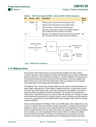
3.11 VPB divider
The VPB Divider determines the relationship between the processor clock (CCLK) and the
clock used by peripheral devices (PCLK). The VPB Divider serves two purposes.
The first is to provides peripherals with desired PCLK via VPB bus so that they can
operate at the speed chosen for the ARM processor. In order to achieve this, the VPB bus
may be slowed down to one half or one fourth of the processor clock rate. Because the
VPB bus must work properly at power up (and its timing cannot be altered if it does not
work since the VPB divider control registers reside on the VPB bus), the default condition
at reset is for the VPB bus to run at one quarter speed.
The second purpose of the VPB Divider is to allow power savings when an application
does not require any peripherals to run at the full processor rate.
The connection of the VPB Divider relative to the oscillator and the processor clock is
shown in Figure 11. Because the VPB Divider is connected to the PLL output, the PLL
remains active (if it was running) during Idle mode.
3.11.1 Register description
Only one register is used to control the VPB Divider.
Table 28:
VPB divider register map
Name
Description
Access Reset
Address
value[1]
VPBDIV
Controls the rate of the VPB clock in relation to
the processor clock.
R/W
[1]
0x00
0xE01F C100
Reset value reflects the data stored in used bits only. It does not include reserved bits content.
3.11.2 VPBDIV register (VPBDIV - 0xE01F C100)
The VPB Divider register contains two bits, allowing three divider values, as shown in
Table 29.
© Koninklijke Philips Electronics N.V. 2005. All rights reserved.
User manual
Rev. 01 — 15 August 2005
40](https://image.slidesharecdn.com/armusrmanl-131212220701-phpapp02/85/Arm-usr-m-anl-40-320.jpg)
![UM10139
Chapter 4: Memory Acceleration Module (MAM)
Rev. 01 — 15 August 2005
User manual
4.1 Introduction
The MAM block in the LPC2141/2/4/6/8 maximizes the performance of the ARM
processor when it is running code in Flash memory, but does so using a single Flash
bank.
4.2 Operation
Simply put, the Memory Accelerator Module (MAM) attempts to have the next ARM
instruction that will be needed in its latches in time to prevent CPU fetch stalls. The
LPC2141/2/4/6/8 uses one bank of Flash memory, compared to the two banks used on
predecessor devices. It includes three 128-bit buffers called the Prefetch Buffer, the
Branch Trail Buffer and the Data Buffer. When an Instruction Fetch is not satisfied by
either the Prefetch or Branch Trail buffer, nor has a prefetch been initiated for that line, the
ARM is stalled while a fetch is initiated for the 128-bit line. If a prefetch has been initiated
but not yet completed, the ARM is stalled for a shorter time. Unless aborted by a data
access, a prefetch is initiated as soon as the Flash has completed the previous access.
The prefetched line is latched by the Flash module, but the MAM does not capture the line
in its prefetch buffer until the ARM core presents the address from which the prefetch has
been made. If the core presents a different address from the one from which the prefetch
has been made, the prefetched line is discarded.
The Prefetch and Branch Trail Buffers each include four 32-bit ARM instructions or eight
16-bit Thumb instructions. During sequential code execution, typically the prefetch buffer
contains the current instruction and the entire Flash line that contains it.
The MAM uses the LPROT[0] line to differentiate between instruction and data accesses.
Code and data accesses use separate 128-bit buffers. 3 of every 4 sequential 32-bit code
or data accesses "hit" in the buffer without requiring a Flash access (7 of 8 sequential
16-bit accesses, 15 of every 16 sequential byte accesses). The fourth (eighth, 16th)
sequential data access must access Flash, aborting any prefetch in progress. When a
Flash data access is concluded, any prefetch that had been in progress is re-initiated.
Timing of Flash read operations is programmable and is described later in this section.
In this manner, there is no code fetch penalty for sequential instruction execution when the
CPU clock period is greater than or equal to one fourth of the Flash access time. The
average amount of time spent doing program branches is relatively small (less than 25%)
and may be minimized in ARM (rather than Thumb) code through the use of the
conditional execution feature present in all ARM instructions. This conditional execution
may often be used to avoid small forward branches that would otherwise be necessary.
Branches and other program flow changes cause a break in the sequential flow of
instruction fetches described above. The Branch Trail Buffer captures the line to which
such a non-sequential break occurs. If the same branch is taken again, the next
instruction is taken from the Branch Trail Buffer. When a branch outside the contents of
© Koninklijke Philips Electronics N.V. 2005. All rights reserved.
User manual
Rev. 01 — 15 August 2005
44](https://image.slidesharecdn.com/armusrmanl-131212220701-phpapp02/85/Arm-usr-m-anl-44-320.jpg)
![UM10139
Philips Semiconductors
Volume 1
Chapter 4: MAM Module
Table 30:
MAM Responses to program accesses of various types
Program Memory Request Type
MAM Mode
0
1
2
Sequential access, data in latches
Initiate Fetch[2]
Use Latched
Data[1]
Use Latched
Data[1]
Sequential access, data not in latches
Initiate Fetch
Initiate Fetch[1]
Initiate Fetch[1]
Non-sequential access, data in latches
Initiate Fetch[2]
Initiate Fetch[1][2] Use Latched
Data[1]
Non-sequential access, data not in latches Initiate Fetch
Initiate Fetch[1]
Initiate Fetch[1]
[1]
Instruction prefetch is enabled in modes 1 and 2.
[2]
The MAM actually uses latched data if it is available, but mimics the timing of a Flash read operation. This
saves power while resulting in the same execution timing. The MAM can truly be turned off by setting the
fetch timing value in MAMTIM to one clock.
Table 31:
MAM responses to data and DMA accesses of various types
Data Memory Request Type
MAM Mode
0
1
Fetch[1]
Sequential access, data in latches
Initiate
Sequential access, data not in latches
Initiate Fetch
Non-sequential access, data in latches
Initiate
Fetch[1]
Non-sequential access, data not in latches Initiate Fetch
[1]
2
Initiate
Fetch[1]
Initiate Fetch
Initiate
Fetch[1]
Initiate Fetch
Use Latched
Data
Initiate Fetch
Use Latched
Data
Initiate Fetch
The MAM actually uses latched data if it is available, but mimics the timing of a Flash read operation. This
saves power while resulting in the same execution timing. The MAM can truly be turned off by setting the
fetch timing value in MAMTIM to one clock.
4.5 MAM configuration
After reset the MAM defaults to the disabled state. Software can turn memory access
acceleration on or off at any time. This allows most of an application to be run at the
highest possible performance, while certain functions can be run at a somewhat slower
but more predictable rate if more precise timing is required.
4.6 Register description
All registers, regardless of size, are on word address boundaries. Details of the registers
appear in the description of each function.
© Koninklijke Philips Electronics N.V. 2005. All rights reserved.
User manual
Rev. 01 — 15 August 2005
47](https://image.slidesharecdn.com/armusrmanl-131212220701-phpapp02/85/Arm-usr-m-anl-47-320.jpg)
![UM10139
Philips Semiconductors
Volume 1
Chapter 4: MAM Module
Table 32:
Name
Summary of MAM registers
Description
Access Reset
Address
value[1]
MAMCR Memory Accelerator Module Control Register.
Determines the MAM functional mode, that is, to
what extent the MAM performance enhancements
are enabled. See Table 33.
R/W
0x0
0xE01F C000
MAMTIM Memory Accelerator Module Timing control.
Determines the number of clocks used for Flash
memory fetches (1 to 7 processor clocks).
R/W
0x07
0xE01F C004
[1]
Reset value reflects the data stored in used bits only. It does not include reserved bits content.
4.7 MAM Control Register (MAMCR - 0xE01F C000)
Two configuration bits select the three MAM operating modes, as shown in Table 33.
Following Reset, MAM functions are disabled. Changing the MAM operating mode causes
the MAM to invalidate all of the holding latches, resulting in new reads of Flash information
as required.
Table 33:
MAM Control Register (MAMCR - address 0xE01F C000) bit description
Bit
Symbol
Value
1:0
MAM_mode 00
_control
01
Description
Reset
value
MAM functions disabled
0
MAM functions partially enabled
10
7:2
Reserved. Not to be used in the application.
-
-
MAM functions fully enabled
11
Reserved, user software should not write ones to reserved NA
bits. The value read from a reserved bit is not defined.
4.8 MAM Timing register (MAMTIM - 0xE01F C004)
The MAM Timing register determines how many CCLK cycles are used to access the
Flash memory. This allows tuning MAM timing to match the processor operating
frequency. Flash access times from 1 clock to 7 clocks are possible. Single clock Flash
accesses would essentially remove the MAM from timing calculations. In this case the
MAM mode may be selected to optimize power usage.
Table 34:
MAM Timing register (MAMTIM - address 0xE01F C004) bit description
Bit
Symbol
Value Description
Reset
value
2:0
MAM_fetch_
cycle_timing
000
0 - Reserved.
07
001
1 - MAM fetch cycles are 1 processor clock (CCLK) in
duration
010
2 - MAM fetch cycles are 2 CCLKs in duration
011
3 - MAM fetch cycles are 3 CCLKs in duration
100
4 - MAM fetch cycles are 4 CCLKs in duration
101
5 - MAM fetch cycles are 5 CCLKs in duration
© Koninklijke Philips Electronics N.V. 2005. All rights reserved.
User manual
Rev. 01 — 15 August 2005
48](https://image.slidesharecdn.com/armusrmanl-131212220701-phpapp02/85/Arm-usr-m-anl-48-320.jpg)
![UM10139
Philips Semiconductors
Volume 1
Table 35:
Chapter 5: VIC
VIC register map
Name
Description
Access
Reset
value[1]
Address
VICIRQStatus
IRQ Status Register. This register reads out the state of
those interrupt requests that are enabled and classified as
IRQ.
RO
0
0xFFFF F000
VICFIQStatus
FIQ Status Requests. This register reads out the state of
those interrupt requests that are enabled and classified as
FIQ.
RO
0
0xFFFF F004
VICRawIntr
Raw Interrupt Status Register. This register reads out the
state of the 32 interrupt requests / software interrupts,
regardless of enabling or classification.
RO
0
0xFFFF F008
VICIntSelect
Interrupt Select Register. This register classifies each of the R/W
32 interrupt requests as contributing to FIQ or IRQ.
0
0xFFFF F00C
VICIntEnable
Interrupt Enable Register. This register controls which of the R/W
32 interrupt requests and software interrupts are enabled to
contribute to FIQ or IRQ.
0
0xFFFF F010
VICIntEnClr
Interrupt Enable Clear Register. This register allows
software to clear one or more bits in the Interrupt Enable
register.
WO
0
0xFFFF F014
VICSoftInt
Software Interrupt Register. The contents of this register are R/W
ORed with the 32 interrupt requests from various peripheral
functions.
0
0xFFFF F018
VICSoftIntClear
Software Interrupt Clear Register. This register allows
software to clear one or more bits in the Software Interrupt
register.
WO
0
0xFFFF F01C
VICProtection
Protection enable register. This register allows limiting
R/W
access to the VIC registers by software running in privileged
mode.
0
0xFFFF F020
VICVectAddr
Vector Address Register. When an IRQ interrupt occurs, the R/W
IRQ service routine can read this register and jump to the
value read.
0
0xFFFF F030
VICDefVectAddr Default Vector Address Register. This register holds the
address of the Interrupt Service routine (ISR) for
non-vectored IRQs.
R/W
0
0xFFFF F034
VICVectAddr0
Vector address 0 register. Vector Address Registers 0-15
hold the addresses of the Interrupt Service routines (ISRs)
for the 16 vectored IRQ slots.
R/W
0
0xFFFF F100
VICVectAddr1
Vector address 1 register.
R/W
0
0xFFFF F104
VICVectAddr2
Vector address 2 register.
R/W
0
0xFFFF F108
VICVectAddr3
Vector address 3 register.
R/W
0
0xFFFF F10C
VICVectAddr4
Vector address 4 register.
R/W
0
0xFFFF F110
VICVectAddr5
Vector address 5 register.
R/W
0
0xFFFF F114
VICVectAddr6
Vector address 6 register.
R/W
0
0xFFFF F118
VICVectAddr7
Vector address 7 register.
R/W
0
0xFFFF F11C
VICVectAddr8
Vector address 8 register.
R/W
0
0xFFFF F120
VICVectAddr9
Vector address 9 register.
R/W
0
0xFFFF F124
VICVectAddr10
Vector address 10 register.
R/W
0
0xFFFF F128
VICVectAddr11
Vector address 11 register.
R/W
0
0xFFFF F12C
© Koninklijke Philips Electronics N.V. 2005. All rights reserved.
User manual
Rev. 01 — 15 August 2005
51](https://image.slidesharecdn.com/armusrmanl-131212220701-phpapp02/85/Arm-usr-m-anl-51-320.jpg)
![UM10139
Philips Semiconductors
Volume 1
Table 35:
Chapter 5: VIC
VIC register map
Name
Description
Access
Reset
value[1]
Address
VICVectAddr12
Vector address 12 register.
R/W
0
0xFFFF F130
VICVectAddr13
Vector address 13 register.
R/W
0
0xFFFF F134
VICVectAddr14
Vector address 14 register.
R/W
0
0xFFFF F138
VICVectAddr15
Vector address 15 register.
R/W
0
0xFFFF F13C
VICVectCntl0
Vector control 0 register. Vector Control Registers 0-15 each R/W
control one of the 16 vectored IRQ slots. Slot 0 has the
highest priority and slot 15 the lowest.
0
0xFFFF F200
VICVectCntl1
Vector control 1 register.
R/W
0
0xFFFF F204
VICVectCntl2
Vector control 2 register.
R/W
0
0xFFFF F208
VICVectCntl3
Vector control 3 register.
R/W
0
0xFFFF F20C
VICVectCntl4
Vector control 4 register.
R/W
0
0xFFFF F210
VICVectCntl5
Vector control 5 register.
R/W
0
0xFFFF F214
VICVectCntl6
Vector control 6 register.
R/W
0
0xFFFF F218
VICVectCntl7
Vector control 7 register.
R/W
0
0xFFFF F21C
VICVectCntl8
Vector control 8 register.
R/W
0
0xFFFF F220
VICVectCntl9
Vector control 9 register.
R/W
0
0xFFFF F224
VICVectCntl10
Vector control 10 register.
R/W
0
0xFFFF F228
VICVectCntl11
Vector control 11 register.
R/W
0
0xFFFF F22C
VICVectCntl12
Vector control 12 register.
R/W
0
0xFFFF F230
VICVectCntl13
Vector control 13 register.
R/W
0
0xFFFF F234
VICVectCntl14
Vector control 14 register.
R/W
0
0xFFFF F238
VICVectCntl15
Vector control 15 register.
R/W
0
0xFFFF F23C
[1]
Reset value reflects the data stored in used bits only. It does not include reserved bits content.
5.4 VIC registers
The following section describes the VIC registers in the order in which they are used in the
VIC logic, from those closest to the interrupt request inputs to those most abstracted for
use by software. For most people, this is also the best order to read about the registers
when learning the VIC.
5.4.1 Software Interrupt register (VICSoftInt - 0xFFFF F018)
The contents of this register are ORed with the 32 interrupt requests from the various
peripherals, before any other logic is applied.
Table 36: Software Interrupt register (VICSoftInt - address 0xFFFF F018) bit allocation
Reset value: 0x0000 0000
Bit
31
30
29
28
27
26
25
24
Symbol
-
-
-
-
-
-
-
-
Access
R/W
R/W
R/W
R/W
R/W
R/W
R/W
R/W
© Koninklijke Philips Electronics N.V. 2005. All rights reserved.
User manual
Rev. 01 — 15 August 2005
52](https://image.slidesharecdn.com/armusrmanl-131212220701-phpapp02/85/Arm-usr-m-anl-52-320.jpg)
![UM10139
Philips Semiconductors
Volume 1
Chapter 5: VIC
5.5 Interrupt sources
Table 57 lists the interrupt sources for each peripheral function. Each peripheral device
has one interrupt line connected to the Vectored Interrupt Controller, but may have several
internal interrupt flags. Individual interrupt flags may also represent more than one
interrupt source.
Table 57:
Connection of interrupt sources to the Vectored Interrupt Controller (VIC)
Block
Flag(s)
VIC Channel # and Hex
Mask
WDT
Watchdog Interrupt (WDINT)
0
0x0000 0001
-
Reserved for Software Interrupts only
1
0x0000 0002
ARM Core
Embedded ICE, DbgCommRx
2
0x0000 0004
ARM Core
Embedded ICE, DbgCommTX
3
0x0000 0008
TIMER0
Match 0 - 3 (MR0, MR1, MR2, MR3)
4
0x0000 0010
5
0x0000 0020
6
0x0000 0040
7
0x0000 0080
Capture 0 - 3 (CR0, CR1, CR2, CR3)
TIMER1
Match 0 - 3 (MR0, MR1, MR2, MR3)
Capture 0 - 3 (CR0, CR1, CR2, CR3)
UART0
Rx Line Status (RLS)
Transmit Holding Register Empty (THRE)
Rx Data Available (RDA)
Character Time-out Indicator (CTI)
UART1
Rx Line Status (RLS)
Transmit Holding Register Empty (THRE)
Rx Data Available (RDA)
Character Time-out Indicator (CTI)
Modem Status Interrupt (MSI)[1]
PWM0
Match 0 - 6 (MR0, MR1, MR2, MR3, MR4, MR5, MR6)
8
0x0000 0100
I2C0
SI (state change)
9
0x0000 0200
SPI0
SPI Interrupt Flag (SPIF)
10
0x0000 0400
11
0x0000 0800
Mode Fault (MODF)
SPI1 (SSP)
TX FIFO at least half empty (TXRIS)
Rx FIFO at least half full (RXRIS)
Receive Timeout condition (RTRIS)
Receive overrun (RORRIS)
PLL
PLL Lock (PLOCK)
12
0x0000 1000
RTC
Counter Increment (RTCCIF)
13
0x0000 2000
External Interrupt 0 (EINT0)
14
0x0000 4000
External Interrupt 1 (EINT1)
15
0x0000 8000
External Interrupt 2 (EINT2)
16
0x0001 0000
Alarm (RTCALF)
System Control
External Interrupt 3 (EINT3)
17
0x0002 0000
ADC0
A/D Converter 0 end of conversion
18
0x0004 0000
I2C1
SI (state change)
19
0x0008 0000
© Koninklijke Philips Electronics N.V. 2005. All rights reserved.
User manual
Rev. 01 — 15 August 2005
59](https://image.slidesharecdn.com/armusrmanl-131212220701-phpapp02/85/Arm-usr-m-anl-59-320.jpg)
![UM10139
Philips Semiconductors
Volume 1
Table 57:
Chapter 5: VIC
Connection of interrupt sources to the Vectored Interrupt Controller (VIC)
Block
Flag(s)
VIC Channel # and Hex
Mask
BOD
Brown Out detect
20
ADC1
A/D Converter 1 end of
USB
[1]
0x0020 0000
22
USB interrupts, DMA interrupt[1]
0x0010 0000
21
conversion[1]
0x0040 0000
LPC2144/6/8 Only.
Interrupt request, masking and selection
nVICFIQIN
SOFTINTCLEAR
[31:0]
SOFTINT
[31:0]
INTENABLE
[31:0]
Non-vectored FIQ interrupt logic
INTENABLECLEAR
[31:0]
VICINT
SOURCE
[31:0]
FIQSTATUS[31:0]
FIQSTATUS
[31:0]
nVICFIQ
Non-vectored IRQ interrupt logic
IRQSTATUS[31:0]
RAWINTERRUPT
[31:0]
Vector interrupt 0
IRQSTATUS
[31:0]
INTSELECT
[31:0]
NonVectIRQ
IRQ
Priority 0
Interrupt priority logic
VECTIRQ0
HARDWARE
PRIORITY
LOGIC
IRQ
nVICIRQ
Address select for
highest priority
interrupt
SOURCE
ENABLE
VECTORCNTL[5:0]
Vector interrupt 1
VECTORADDR
[31:0]
Priority1
VECTADDR0[31:0]
VECTIRQ1
VECTORADDR
[31:0]
VECTADDR1[31:0]
VICVECT
ADDROUT
[31:0]
Priority2
Vector interrupt 15
Priority14
VECTIRQ15
DEFAULT
VECTORADDR
[31:0]
VECTADDR15[31:0]
Priority15
nVICIRQIN
VICVECTADDRIN[31:0]
Fig 13. Block diagram of the Vectored Interrupt Controller (VIC)
© Koninklijke Philips Electronics N.V. 2005. All rights reserved.
User manual
Rev. 01 — 15 August 2005
60](https://image.slidesharecdn.com/armusrmanl-131212220701-phpapp02/85/Arm-usr-m-anl-60-320.jpg)
![UM10139
Philips Semiconductors
Volume 1
Chapter 5: VIC
do and how to process the interrupt request. However, it is recommended that only one
interrupt source should be classified as FIQ. Classifying more than one interrupt sources
as FIQ will increase the interrupt latency.
Following the completion of the desired interrupt service routine, clearing of the interrupt
flag on the peripheral level will propagate to corresponding bits in VIC registers
(VICRawIntr, VICFIQStatus and VICIRQStatus). Also, before the next interrupt can be
serviced, it is necessary that write is performed into the VICVectAddr register before the
return from interrupt is executed. This write will clear the respective interrupt flag in the
internal interrupt priority hardware.
In order to disable the interrupt at the VIC you need to clear corresponding bit in the
VICIntEnClr register, which in turn clears the related bit in the VICIntEnable register. This
also applies to the VICSoftInt and VICSoftIntClear in which VICSoftIntClear will clear the
respective bits in VICSoftInt. For example, if VICSoftInt = 0x0000 0005 and bit 0 has to be
cleared, VICSoftIntClear = 0x0000 0001 will accomplish this. Before the new clear
operation on the same bit in VICSoftInt using writing into VICSoftIntClear is performed in
the future, VICSoftIntClear = 0x0000 0000 must be assigned. Therefore writing 1 to any
bit in Clear register will have one-time-effect in the destination register.
If the watchdog is enabled for interrupt on underflow or invalid feed sequence only then
there is no way of clearing the interrupt. The only way you could perform return from
interrupt is by disabling the interrupt at the VIC (using VICIntEnClr).
Example:
Assuming that UART0 and SPI0 are generating interrupt requests that are classified as
vectored IRQs (UART0 being on the higher level than SPI0), while UART1 and I2C are
generating non-vectored IRQs, the following could be one possibility for VIC setup:
VICIntSelect = 0x0000 0000
VICIntEnable = 0x0000 06C0
VICDefVectAddr = 0x...
VICVectAddr0 = 0x...
VICVectAddr1 = 0x...
VICVectCntl0 = 0x0000 0026
VICVectCntl1 = 0x0000 002A
; SPI0, I2C, UART1 and UART0 are IRQ =>
; bit10, bit9, bit7 and bit6=0
; SPI0, I2C, UART1 and UART0 are enabled interrupts =>
; bit10, bit9, bit 7 and bit6=1
; holds address at what routine for servicing
; non-vectored IRQs (i.e. UART1 and I2C) starts
; holds address where UART0 IRQ service routine starts
; holds address where SPI0 IRQ service routine starts
; interrupt source with index 6 (UART0) is enabled as
; the one with priority 0 (the highest)
; interrupt source with index 10 (SPI0) is enabled
; as the one with priority 1
After any of IRQ requests (SPI0, I2C, UART0 or UART1) is made, microcontroller will
redirect code execution to the address specified at location 0x0000 0018. For vectored
and non-vectored IRQ’s the following instruction could be placed at 0x0000 0018:
LDR pc, [pc,#-0xFF0]
This instruction loads PC with the address that is present in VICVectAddr register.
© Koninklijke Philips Electronics N.V. 2005. All rights reserved.
User manual
Rev. 01 — 15 August 2005
64](https://image.slidesharecdn.com/armusrmanl-131212220701-phpapp02/85/Arm-usr-m-anl-64-320.jpg)
![UM10139
Philips Semiconductors
Volume 1
Table 58:
Pin description
Symbol
Pin
Chapter 6: Pin Configuration
Description
I/O
P0.0 to P0.31
Type
Port 0: Port 0 is a 32-bit I/O port with individual direction controls for each bit.
Total of 28 pins of the Port 0 can be used as a general purpose bi-directional
digital I/Os while P0.31 provides digital output functions only. The operation of
port 0 pins depends upon the pin function selected via the pin connect block.
Pins P0.24, P0.26 and P0.27 are not available.
P0.0/TXD0/
PWM1
19[1]
P0.1/RxD0/
PWM3/EINT0
21[2]
P0.3 — General purpose digital input/output pin
SDA0 — I2C0 data input/output. Open drain output (for I2C compliance)
MAT0.0 — Match output for Timer 0, channel 0
EINT1 — External interrupt 1 input
I/O
P0.4 — General purpose digital input/output pin
I/O
SCK0 — Serial clock for SPI0. SPI clock output from master or input to slave
CAP0.1 — Capture input for Timer 0, channel 0
I
AD0.6 — A/D converter 0, input 6. This analog input is always connected to
its pin
I/O
P0.5 — General purpose digital input/output pin
I/O
MISO0 — Master In Slave OUT for SPI0. Data input to SPI master or data
output from SPI slave
O
MAT0.1 — Match output for Timer 0, channel 1
I
AD0.7 — A/D converter 0, input 7. This analog input is always connected to
its pin
I/O
P0.6 — General purpose digital input/output pin
I/O
MOSI0 — Master Out Slave In for SPI0. Data output from SPI master or data
input to SPI slave
I
CAP0.2 — Capture input for Timer 0, channel 2
I
AD1.0 — A/D converter 1, input 0. This analog input is always connected to
its pin. Available in LPC2144/6/8 only.
I/O
P0.7 — General purpose digital input/output pin
I
SSEL0 — Slave Select for SPI0. Selects the SPI interface as a slave
O
PWM2 — Pulse Width Modulator output 2
I
31[2]
I/O
I
P0.7/SSEL0/
PWM2/EINT2
CAP0.0 — Capture input for Timer 0, channel 0
I/O
30[4]
SCL0 — I2C0 clock input/output. Open drain output (for I2C compliance)
I
P0.6/MOSI0/
CAP0.2/AD1.0
P0.2 — General purpose digital input/output pin
I/O
29[4]
EINT0 — External interrupt 0 input
I/O
O
P0.5/MISO0/
MAT0.1/AD0.7
PWM3 — Pulse Width Modulator output 3
I
P0.4/SCK0/
CAP0.1/AD0.6
RxD0 — Receiver input for UART0
I
27[4]
P0.1 — General purpose digital input/output pin
O
P0.3/SDA0/
MAT0.0/EINT1
PWM1 — Pulse Width Modulator output 1
I/O
I
26[3]
TXD0 — Transmitter output for UART0
O
22[3]
P0.0 — General purpose digital input/output pin
O
P0.2/SCL0/
CAP0.0
I/O
EINT2 — External interrupt 2 input
© Koninklijke Philips Electronics N.V. 2005. All rights reserved.
User manual
Rev. 01 — 15 August 2005
69](https://image.slidesharecdn.com/armusrmanl-131212220701-phpapp02/85/Arm-usr-m-anl-69-320.jpg)
![UM10139
Philips Semiconductors
Volume 1
Table 58:
Chapter 6: Pin Configuration
Pin description …continued
Symbol
Pin
Type
Description
P0.8/TXD1/
PWM4/AD1.1
33[4]
I/O
P0.8 — General purpose digital input/output pin
O
TXD1 — Transmitter output for UART1
O
PWM4 — Pulse Width Modulator output 4
I
AD1.1 — A/D converter 1, input 1. This analog input is always connected to
its pin. Available in LPC2144/6/8 only
I/O
P0.9 — General purpose digital input/output pin
I
RxD1 — Receiver input for UART1
O
PWM6 — Pulse Width Modulator output 6
I
EINT3 — External interrupt 3 input
I/O
P0.10 — General purpose digital input/output pin
O
RTS1 — Request to Send output for UART1. Available in LPC2144/6/8 only.
I
CAP1.0 — Capture input for Timer 1, channel 0
I
AD1.2 — A/D converter 1, input 2. This analog input is always connected to
its pin. Available in LPC2144/6/8 only.
I/O
P0.11 — General purpose digital input/output pin
I
CTS1 — Clear to Send input for UART1. Available in LPC2144/6/8 only.
I
CAP1.1 — Capture input for Timer 1, channel 1.
I/O
SCL1 — I2C1 clock input/output. Open drain output (for I2C compliance)
I/O
P0.12 — General purpose digital input/output pin
I
DSR1 — Data Set Ready input for UART1. Available in LPC2144/6/8 only.
O
MAT1.0 — Match output for Timer 1, channel 0.
I
AD1.3 — A/D converter input 3. This analog input is always connected to its
pin. Available in LPC2144/6/8 only.
I/O
P0.13 — General purpose digital input/output pin
O
DTR1 — Data Terminal Ready output for UART1. Available in LPC2144/6/8
only.
O
MAT1.1 — Match output for Timer 1, channel 1.
I
AD1.4 — A/D converter input 4. This analog input is always connected to its
pin. Available in LPC2144/6/8 only.
I/O
P0.14 — General purpose digital input/output pin
I
DCD1 — Data Carrier Detect input for UART1. Available in LPC2144/6/8 only.
I
EINT1 — External interrupt 1 input
I/O
SDA1 — I2C1 data input/output. Open drain output (for I2C compliance)
P0.9/RxD1/
PWM6/EINT3
P0.10/RTS1/
CAP1.0/AD1.2
P0.11/CTS1/
CAP1.1/SCL1
P0.12/DSR1/
MAT1.0/AD1.3
P0.13/DTR1/
MAT1.1/AD1.4
P0.14/DCD1/
EINT1/SDA1
34[2]
35[4]
37[3]
38[4]
39[4]
41[3]
Note: LOW on this pin while RESET is LOW forces on-chip boot-loader to
take over control of the part after reset.
P0.15/RI1/
EINT2/AD1.5
45[4]
I/O
P0.15 — General purpose digital input/output pin
I
RI1 — Ring Indicator input for UART1. Available in LPC2144/6/8 only.
I
EINT2 — External interrupt 2 input.
I
AD1.5 — A/D converter 1, input 5. This analog input is always connected to
its pin. Available in LPC2144/6/8 only.
© Koninklijke Philips Electronics N.V. 2005. All rights reserved.
User manual
Rev. 01 — 15 August 2005
70](https://image.slidesharecdn.com/armusrmanl-131212220701-phpapp02/85/Arm-usr-m-anl-70-320.jpg)
![UM10139
Philips Semiconductors
Volume 1
Table 58:
Chapter 6: Pin Configuration
Pin description …continued
Symbol
Pin
MISO1 — Master In Slave Out for SSP. Data input to SPI master or data
output from SSP slave.
MAT1.3 — Match output for Timer 1, channel 3.
I/O
P0.19 — General purpose digital input/output pin
MAT1.2 — Match output for Timer 1, channel 2.
MOSI1 — Master Out Slave In for SSP. Data output from SSP master or data
input to SSP slave.
CAP1.2 — Capture input for Timer 1, channel 2.
I/O
P0.20 — General purpose digital input/output pin
MAT1.3 — Match output for Timer 1, channel 3.
SSEL1 — Slave Select for SSP. Selects the SSP interface as a slave.
EINT3 — External interrupt 3 input.
I/O
P0.21 — General purpose digital input/output pin
PWM5 — Pulse Width Modulator output 5.
I
AD1.6 — A/D converter 1, input 6. This analog input is always connected to
its pin. Available in LPC2144/6/8 only.
I
CAP1.3 — Capture input for Timer 1, channel 3.
I/O
P0.22 — General purpose digital input/output pin.
I
AD1.7 — A/D converter 1, input 7. This analog input is always connected to
its pin. Available in LPC2144/6/8 only.
I
CAP0.0 — Capture input for Timer 0, channel 0.
O
MAT0.0 — Match output for Timer 0, channel 0.
I/O
P0.23 — General purpose digital input/output pin.
I
VBUS — Indicates the presence of USB bus power.
I/O
P0.25 — General purpose digital input/output pin
I
AD0.4 — A/D converter 0, input 4. This analog input is always connected to
its pin.
O
P0.25/AD0.4/
Aout
CAP1.3 — Capture input for Timer 1, channel 3.
O
9[5]
P0.18 — General purpose digital input/output pin
I
58[1]
I/O
I
P0.23
MAT1.2 — Match output for Timer 1, channel 2.
O
P0.22/AD1.7/
2[4]
CAP0.0/MAT0.0
SCK1 — Serial Clock for SSP. Clock output from master or input to slave.
I
P0.21/PWM5/
AD1.6/CAP1.3
CAP1.2 — Capture input for Timer 1, channel 2.
O
1[4]
P0.17 — General purpose digital input/output pin
I/O
P0.20/MAT1.3/
SSEL1/EINT3
I/O
O
55[2]
CAP0.2 — Capture input for Timer 0, channel 2.
I/O
P0.19/MAT1.2/
MOSI1/CAP1.2
MAT0.2 — Match output for Timer 0, channel 2.
I
54[1]
EINT0 — External interrupt 0 input.
O
53[1]
I
I/O
P0.18/CAP1.3/
MISO1/MAT1.3
P0.16 — General purpose digital input/output pin
I
47[1]
I/O
I
P0.17/CAP1.2/
SCK1/MAT1.2
Description
O
P0.16/EINT0/
46[2]
MAT0.2/CAP0.2
Type
Aout — D/A converter output. Available in LPC2142/4/6/8 only.
© Koninklijke Philips Electronics N.V. 2005. All rights reserved.
User manual
Rev. 01 — 15 August 2005
71](https://image.slidesharecdn.com/armusrmanl-131212220701-phpapp02/85/Arm-usr-m-anl-71-320.jpg)
![UM10139
Philips Semiconductors
Volume 1
Table 58:
Chapter 6: Pin Configuration
Pin description …continued
Symbol
Pin
MAT0.2 — Match output for Timer 0, channel 2.
I/O
P0.29 — General purpose digital input/output pin
AD0.2 — A/D converter 0, input 2. This analog input is always connected to
its pin.
CAP0.3 — Capture input for Timer 0, Channel 3.
MAT0.3 — Match output for Timer 0, channel 3.
I/O
P0.30 — General purpose digital input/output pin.
I
AD0.3 — A/D converter 0, input 3. This analog input is always connected to
its pin.
EINT3 — External interrupt 3 input.
I
CAP0.0 — Capture input for Timer 0, channel 0.
O
P0.31 — General purpose output only digital pin (GPO).
O
UP_LED — USB Good Link LED indicator. It is LOW when device is
configured (non-control endpoints enabled). It is HIGH when the device is not
configured or during global suspend.
O
17[6]
CAP0.2 — Capture input for Timer 0, channel 2.
I
P0.31
AD0.1 — A/D converter 0, input 1. This analog input is always connected to
its pin.
O
P0.30/AD0.3/
EINT3/CAP0.0
I
I
15[4]
P0.28 — General purpose digital input/output pin
I
P0.29/AD0.2/
CAP0.3/MAT0.3
I/O
O
14[4]
Description
I
P0.28/AD0.1/
13[4]
CAP0.2/MAT0.2
Type
CONNECT — Signal used to switch an external 1.5 kΩ resistor under the
software control (active state for this signal is LOW). Used with the Soft
Connect USB feature.
Note: This pin MUST NOT be externally pulled LOW when RESET pin is
LOW or the JTAG port will be disabled.
P1.0 to P1.31
I/O
P1.19/
TRACEPKT3
4[6]
P1.20/
TRACESYNC
48[6]
P1.17 — General purpose digital input/output pin
TRACEPKT1 — Trace Packet, bit 1. Standard I/O port with internal pull-up.
I/O
P1.18 — General purpose digital input/output pin
TRACEPKT2 — Trace Packet, bit 2. Standard I/O port with internal pull-up.
I/O
P1.19 — General purpose digital input/output pin
TRACEPKT3 — Trace Packet, bit 3. Standard I/O port with internal pull-up.
I/O
P1.20 — General purpose digital input/output pin
O
P1.18/
TRACEPKT2
8[6]
TRACEPKT0 — Trace Packet, bit 0. Standard I/O port with internal pull-up.
O
12[6]
I/O
O
P1.17/
TRACEPKT1
P1.16 — General purpose digital input/output pin
O
16[6]
I/O
O
P1.16/
TRACEPKT0
Port 1: Port 1 is a 32-bit bi-directional I/O port with individual direction
controls for each bit. The operation of port 1 pins depends upon the pin
function selected via the pin connect block. Pins 0 through 15 of port 1 are not
available.
TRACESYNC — Trace Synchronization. Standard I/O port with internal
pull-up.
Note: LOW on this pin while RESET is LOW enables pins P1.25:16 to
operate as Trace port after reset
P1.21/
PIPESTAT0
44[6]
I/O
P1.21 — General purpose digital input/output pin
O
PIPESTAT0 — Pipeline Status, bit 0. Standard I/O port with internal pull-up.
© Koninklijke Philips Electronics N.V. 2005. All rights reserved.
User manual
Rev. 01 — 15 August 2005
72](https://image.slidesharecdn.com/armusrmanl-131212220701-phpapp02/85/Arm-usr-m-anl-72-320.jpg)
![UM10139
Philips Semiconductors
Volume 1
Table 58:
Chapter 6: Pin Configuration
Pin description …continued
Symbol
Pin
Type
Description
P1.22/
PIPESTAT1
40[6]
I/O
P1.22 — General purpose digital input/output pin
O
PIPESTAT1 — Pipeline Status, bit 1. Standard I/O port with internal pull-up.
P1.23/
PIPESTAT2
36[6]
I/O
P1.23 — General purpose digital input/output pin
O
PIPESTAT2 — Pipeline Status, bit 2. Standard I/O port with internal pull-up.
P1.24/
TRACECLK
32[6]
I/O
P1.24 — General purpose digital input/output pin
O
TRACECLK — Trace Clock. Standard I/O port with internal pull-up.
P1.25/EXTIN0
28[6]
I/O
P1.25 — General purpose digital input/output pin
I
EXTIN0 — External Trigger Input. Standard I/O with internal pull-up.
I/O
P1.26 — General purpose digital input/output pin
I/O
RTCK — Returned Test Clock output. Extra signal added to the JTAG port.
Assists debugger synchronization when processor frequency varies.
Bi-directional pin with internal pull-up.
P1.26/RTCK
24[6]
Note: LOW on this pin while RESET is LOW enables pins P1.31:26 to
operate as Debug port after reset
P1.27/TDO
64[6]
P1.28/TDI
60[6]
P1.29/TCK
56[6]
P1.30/TMS
52[6]
P1.31/TRST
20[6]
D+
10[7]
D-
10[7]
RESET
57[8]
XTAL1
I/O
P1.27 — General purpose digital input/output pin
O
TDO — Test Data out for JTAG interface.
I/O
P1.28 — General purpose digital input/output pin
I
TDI — Test Data in for JTAG interface.
I/O
P1.29 — General purpose digital input/output pin
I
TCK — Test Clock for JTAG interface.
I/O
P1.30 — General purpose digital input/output pin
I
TMS — Test Mode Select for JTAG interface.
I/O
P1.31 — General purpose digital input/output pin
I
TRST — Test Reset for JTAG interface.
I/O
USB bidirectional D+ line.
I/O
USB bidirectional D- line.
I
External reset input: A LOW on this pin resets the device, causing I/O ports
and peripherals to take on their default states, and processor execution to
begin at address 0. TTL with hysteresis, 5 V tolerant.
62[9]
I
Input to the oscillator circuit and internal clock generator circuits.
XTAL2
61[9]
O
Output from the oscillator amplifier.
RTXC1
3[9]
I
Input to the RTC oscillator circuit.
RTXC2
5[9]
O
Output from the RTC oscillator circuit.
VSS
6, 18, 25, 42, I
50
Ground: 0 V reference
VSSA
59
I
Analog Ground: 0 V reference. This should nominally be the same voltage
as VSS, but should be isolated to minimize noise and error.
VDD
23, 43, 51
I
3.3 V Power Supply: This is the power supply voltage for the core and I/O
ports.
© Koninklijke Philips Electronics N.V. 2005. All rights reserved.
User manual
Rev. 01 — 15 August 2005
73](https://image.slidesharecdn.com/armusrmanl-131212220701-phpapp02/85/Arm-usr-m-anl-73-320.jpg)
![UM10139
Philips Semiconductors
Volume 1
Table 58:
Chapter 6: Pin Configuration
Pin description …continued
Symbol
Pin
Type
Description
VDDA
7
I
Analog 3.3 V Power Supply: This should be nominally the same voltage as
VDD but should be isolated to minimize noise and error. This voltage is used to
power the ADC(s).
VREF
63
I
A/D Converter Reference: This should be nominally the same voltage as
VDD but should be isolated to minimize noise and error. Level on this pin is
used as a reference for A/D convertor.
VBAT
49
I
RTC Power Supply: 3.3 V on this pin supplies the power to the RTC.
[1]
5 V tolerant pad providing digital I/O functions with TTL levels and hysteresis and 10 ns slew rate control.
[2]
5 V tolerant pad providing digital I/O functions with TTL levels and hysteresis and 10 ns slew rate control. If
configured for an input function, this pad utilizes built-in glitch filter that blocks pulses shorter than 3 ns.
[3]
Open-drain 5 V tolerant digital I/O I2C-bus 400 kHz specification compatible pad. It requires external pull-up
to provide an output functionality.
[4]
5 V tolerant pad providing digital I/O (with TTL levels and hysteresis and 10 ns slew rate control) and analog
input function. If configured for an input function, this pad utilizes built-in glitch filter that blocks pulses
shorter than 3 ns. When configured as an ADC input, digital section of the pad is disabled.
[5]
5 V tolerant pad providing digital I/O (with TTL levels and hysteresis and 10 ns slew rate control) and analog
output function. When configured as the DAC output, digital section of the pad is disabled.
[6]
5 V tolerant pad with built-in pull-up resistor providing digital I/O functions with TTL levels and hysteresis
and 10 ns slew rate control. The pull-up resistor’s value typically ranges from 60 kΩ to 300 kΩ.
[7]
Pad is designed in accordance with the Universal Serial Bus (USB) specification, revision 2.0 (Full-speed
and Low-speed mode only).
[8]
5 V tolerant pad providing digital input (with TTL levels and hysteresis) function only.
[9]
Pad provides special analog functionality.
© Koninklijke Philips Electronics N.V. 2005. All rights reserved.
User manual
Rev. 01 — 15 August 2005
74](https://image.slidesharecdn.com/armusrmanl-131212220701-phpapp02/85/Arm-usr-m-anl-74-320.jpg)
![UM10139
Chapter 7: Pin Connect Block
Rev. 01 — 15 August 2005
User manual
7.1 Features
• Allows individual pin configuration.
7.2 Applications
The purpose of the Pin Connect Block is to configure the microcontroller pins to the
desired functions.
7.3 Description
The pin connect block allows selected pins of the microcontroller to have more than one
function. Configuration registers control the multiplexers to allow connection between the
pin and the on chip peripherals.
Peripherals should be connected to the appropriate pins prior to being activated, and prior
to any related interrupt(s) being enabled. Activity of any enabled peripheral function that is
not mapped to a related pin should be considered undefined.
Selection of a single function on a port pin completely excludes all other functions
otherwise available on the same pin.
The only partial exception from the above rule of exclusion is the case of inputs to the A/D
converter. Regardless of the function that is selected for the port pin that also hosts the
A/D input, this A/D input can be read at any time and variations of the voltage level on this
pin will be reflected in the A/D readings. However, valid analog reading(s) can be obtained
if and only if the function of an analog input is selected. Only in this case proper interface
circuit is active in between the physical pin and the A/D module. In all other cases, a part
of digital logic necessary for the digital function to be performed will be active, and will
disrupt proper behavior of the A/D.
7.4 Register description
The Pin Control Module contains 2 registers as shown in Table 59 below.
Table 59:
Pin connect block register map
Reset value[1]
Address
Pin function select Read/Write
register 0.
0x0000 0000
0xE002 C000
PINSEL1
Pin function select Read/Write
register 1.
0x0000 0000
0xE002 C004
PINSEL2
Pin function select Read/Write
register 2.
See Table 62
0xE002 C014
Name
Description
PINSEL0
[1]
Access
Reset value reflects the data stored in used bits only. It does not include reserved bits content.
© Koninklijke Philips Electronics N.V. 2005. All rights reserved.
User manual
Rev. 01 — 15 August 2005
75](https://image.slidesharecdn.com/armusrmanl-131212220701-phpapp02/85/Arm-usr-m-anl-75-320.jpg)
![UM10139
Philips Semiconductors
Volume 1
Chapter 7: Pin Connect Block
7.4.1 Pin Function Select Register 0 (PINSEL0 - 0xE002 C000)
The PINSEL0 register controls the functions of the pins as per the settings listed in
Table 63. The direction control bit in the IO0DIR register is effective only when the GPIO
function is selected for a pin. For other functions, direction is controlled automatically.
Table 60:
Pin function Select register 0 (PINSEL0 - address 0xE002 C000) bit description
Bit
Symbol
Value
Function
Reset value
1:0
P0.0
00
GPIO Port 0.0
0
01
TXD (UART0)
10
PWM1
11
Reserved
00
GPIO Port 0.1
01
RxD (UART0)
10
PWM3
11
EINT0
00
GPIO Port 0.2
01
SCL0 (I2C0)
10
Capture 0.0 (Timer 0)
11
Reserved
00
GPIO Port 0.3
01
SDA0 (I2C0)
10
Match 0.0 (Timer 0)
11
EINT1
00
GPIO Port 0.4
01
SCK0 (SPI0)
10
Capture 0.1 (Timer 0)
11
AD0.6
00
GPIO Port 0.5
01
MISO0 (SPI0)
10
Match 0.1 (Timer 0)
11
AD0.7
00
GPIO Port 0.6
01
MOSI0 (SPI0)
10
Capture 0.2 (Timer 0)
11
Reserved[1][2] or AD1.0[3]
00
GPIO Port 0.7
01
SSEL0 (SPI0)
10
PWM2
11
EINT2
00
GPIO Port 0.8
01
TXD UART1
10
PWM4
11
Reserved[1][2] or AD1.1[3]
3:2
5:4
7:6
9:8
11:10
13:12
15:14
17:16
P0.1
P0.2
P0.3
P0.4
P0.5
P0.6
P0.7
P0.8
0
0
0
0
0
0
0
0
© Koninklijke Philips Electronics N.V. 2005. All rights reserved.
User manual
Rev. 01 — 15 August 2005
76](https://image.slidesharecdn.com/armusrmanl-131212220701-phpapp02/85/Arm-usr-m-anl-76-320.jpg)
![UM10139
Philips Semiconductors
Volume 1
Chapter 7: Pin Connect Block
Table 60:
Pin function Select register 0 (PINSEL0 - address 0xE002 C000) bit description
Bit
Symbol
Value
Function
Reset value
19:18
P0.9
00
GPIO Port 0.9
0
01
RxD (UART1)
10
PWM6
11
EINT3
00
GPIO Port 0.10
01
Reserved[1][2]
10
Capture 1.0 (Timer 1)
11
Reserved[1][2] or AD1.2[3]
00
GPIO Port 0.11
01
Reserved[1][2]
10
Capture 1.1 (Timer 1)
11
SCL1 (I2C1)
00
GPIO Port 0.12
01
Reserved[1][2]
10
Match 1.0 (Timer 1)
11
Reserved[1][2] or AD1.3[3]
00
GPIO Port 0.13
01
Reserved[1][2]
10
Match 1.1 (Timer 1)
11
Reserved[1][2] or AD1.4[3]
00
GPIO Port 0.14
01
Reserved[1][2]
10
EINT1
11
SDA1 (I2C1)
00
GPIO Port 0.15
01
Reserved[1][2]
10
EINT2
11
Reserved[1][2] or AD1.5[3]
21:20
23:22
25:24
27:26
29:28
31:30
P0.10
P0.11
P0.12
P0.13
P0.14
P0.15
[1]
0
or CTS
0
or DSR
(UART1)[3]
0
or DTR
(UART1)[3]
0
or DCD
or RI
(UART1)[3]
(UART1)[3]
0
(UART1)[3]
Available on LPC2142.
[3]
or RTS
Available on LPC2141.
[2]
0
(UART1)[3]
Available on LPC2144/6/8.
7.4.2 Pin function Select register 1 (PINSEL1 - 0xE002 C004)
The PINSEL1 register controls the functions of the pins as per the settings listed in
following tables. The direction control bit in the IO0DIR register is effective only when the
GPIO function is selected for a pin. For other functions direction is controlled
automatically.
© Koninklijke Philips Electronics N.V. 2005. All rights reserved.
User manual
Rev. 01 — 15 August 2005
77](https://image.slidesharecdn.com/armusrmanl-131212220701-phpapp02/85/Arm-usr-m-anl-77-320.jpg)
![UM10139
Philips Semiconductors
Volume 1
Chapter 7: Pin Connect Block
Table 61:
Pin function Select register 1 (PINSEL1 - address 0xE002 C004) bit description
Bit
Symbol
Value
Function
Reset value
1:0
P0.16
00
GPIO Port 0.16
0
01
EINT0
10
Match 0.2 (Timer 0)
11
Capture 0.2 (Timer 0)
00
GPIO Port 0.17
01
Capture 1.2 (Timer 1)
10
SCK1 (SSP)
11
Match 1.2 (Timer 1)
00
GPIO Port 0.18
01
Capture 1.3 (Timer 1)
10
MISO1 (SSP)
11
Match 1.3 (Timer 1)
00
GPIO Port 0.19
01
Match 1.2 (Timer 1)
10
MOSI1 (SSP)
11
Capture 1.2 (Timer 1)
00
GPIO Port 0.20
01
Match 1.3 (Timer 1)
10
SSEL1 (SSP)
11
EINT3
00
GPIO Port 0.21
01
PWM5
10
Reserved[1][2] or AD1.6[3]
11
Capture 1.3 (Timer 1)
00
GPIO Port 0.22
01
Reserved[1][2] or AD1.7[3]
10
Capture 0.0 (Timer 0)
11
Match 0.0 (Timer 0)
00
GPIO Port 0.23
01
VBUS
10
Reserved
11
Reserved
00
Reserved
01
Reserved
10
Reserved
11
Reserved
00
GPIO Port 0.25
01
AD0.4
10
Reserved[1] or Aout(DAC)[2][3]
11
Reserved
3:2
5:4
7:6
9:8
11:10
13:12
15:14
17:16
19:18
P0.17
P0.18
P0.19
P0.20
P0.21
P0.22
P0.23
P0.24
P0.25
0
0
0
0
0
0
0
0
0
© Koninklijke Philips Electronics N.V. 2005. All rights reserved.
User manual
Rev. 01 — 15 August 2005
78](https://image.slidesharecdn.com/armusrmanl-131212220701-phpapp02/85/Arm-usr-m-anl-78-320.jpg)
![UM10139
Philips Semiconductors
Volume 1
Chapter 7: Pin Connect Block
Table 61:
Pin function Select register 1 (PINSEL1 - address 0xE002 C004) bit description
Bit
Symbol
Value
Function
Reset value
21:20
P0.26
00
Reserved
0
01
Reserved
10
Reserved
11
Reserved
00
Reserved
01
Reserved
10
Reserved
11
Reserved
00
GPIO Port 0.28
01
AD0.1
10
Capture 0.2 (Timer 0)
11
Match 0.2 (Timer 0)
00
GPIO Port 0.29
01
AD0.2
10
Capture 0.3 (Timer 0)
11
Match 0.3 (Timer 0)
00
GPIO Port 0.30
01
AD0.3
10
EINT3
11
Capture 0.0 (Timer 0)
00
GPO Port only
01
UP_LED
10
CONNECT
11
Reserved
23:22
25:24
27:26
29:28
31:30
P0.27
P0.28
P0.29
P0.30
P0.31
[1]
0
0
0
Available on LPC2142.
[3]
0
Available on LPC2141.
[2]
0
Available on LPC2144/6/8.
7.4.3 Pin function Select register 2 (PINSEL2 - 0xE002 C014)
The PINSEL2 register controls the functions of the pins as per the settings listed in
Table 62. The direction control bit in the IO1DIR register is effective only when the GPIO
function is selected for a pin. For other functions direction is controlled automatically.
Warning: use read-modify-write operation when accessing PINSEL2 register. Accidental
write of 0 to bit 2 and/or bit 3 results in loss of debug and/or trace functionality! Changing
of either bit 4 or bit 5 from 1 to 0 may cause an incorrect code execution!
© Koninklijke Philips Electronics N.V. 2005. All rights reserved.
User manual
Rev. 01 — 15 August 2005
79](https://image.slidesharecdn.com/armusrmanl-131212220701-phpapp02/85/Arm-usr-m-anl-79-320.jpg)
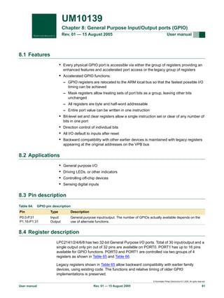
![UM10139
Philips Semiconductors
Volume 1
Chapter 8: GPIO
The registers in Table 66 represent the enhanced GPIO features available on the
LPC2141/2/4/6/8. All of these registers are located directly on the local bus of the CPU for
the fastest possible read and write timing. An additional feature has been added that
provides byte addressability of all GPIO registers. A mask register allows treating groups
of bits in a single GPIO port separately from other bits on the same port.
User must select whether a GPIO will be accessed via registers that provide enhanced
features or a legacy set of registers (see Section 3.6.1 “System Control and Status flags
register (SCS - 0xE01F C1A0)” on page 26). While both of a port’s fast and legacy GPIO
registers are controlling the same physical pins, these two port control branches are
mutually exclusive and operate independently. For example, changing a pin’s output via a
fast register will not be observable via the corresponding legacy register.
The following text will refer to the legacy GPIO as "the slow" GPIO, while GPIO equipped
with the enhanced features will be referred as "the fast" GPIO.
Table 65:
GPIO register map (legacy VPB accessible registers)
Generic
Name
Description
IOPIN
GPIO Port Pin value register. The current
R/W
state of the GPIO configured port pins can
always be read from this register, regardless
of pin direction.
NA
0xE002 8000
IO0PIN
0xE002 8010
IO1PIN
IOSET
GPIO Port Output Set register. This register
controls the state of output pins in
conjunction with the IOCLR register. Writing
ones produces highs at the corresponding
port pins. Writing zeroes has no effect.
R/W
0x0000 0000 0xE002 8004
IO0SET
0xE002 8014
IO1SET
IODIR
GPIO Port Direction control register. This
register individually controls the direction of
each port pin.
R/W
0x0000 0000 0xE002 8008
IO0DIR
0xE002 8018
IO1DIR
IOCLR
GPIO Port Output Clear register. This
register controls the state of output pins.
Writing ones produces lows at the
corresponding port pins and clears the
corresponding bits in the IOSET register.
Writing zeroes has no effect.
WO
0x0000 0000 0xE002 800C
IO0CLR
0xE002 801C
IO1CLR
[1]
Access Reset
value[1]
PORT0
PORT1
Address & Name Address & Name
Reset value reflects the data stored in used bits only. It does not include reserved bits content.
© Koninklijke Philips Electronics N.V. 2005. All rights reserved.
User manual
Rev. 01 — 15 August 2005
82](https://image.slidesharecdn.com/armusrmanl-131212220701-phpapp02/85/Arm-usr-m-anl-82-320.jpg)
![UM10139
Philips Semiconductors
Volume 1
Table 66:
Chapter 8: GPIO
GPIO register map (local bus accessible registers - enhanced GPIO features)
Generic
Name
Description
Access Reset
value[1]
FIODIR
Fast GPIO Port Direction control register.
This register individually controls the
direction of each port pin.
R/W
0x0000 0000 0x3FFF C000
FIO0DIR
0x3FFF C020
FIO1DIR
FIOMASK
Fast Mask register for port. Writes, sets,
R/W
clears, and reads to port (done via writes to
FIOPIN, FIOSET, and FIOCLR, and reads of
FIOPIN) alter or return only the bits enabled
by zeros in this register.
0x0000 0000 0x3FFF C010
FIO0MASK
0x3FFF C030
FIO1MASK
FIOPIN
Fast Port Pin value register using FIOMASK. R/W
The current state of digital port pins can be
read from this register, regardless of pin
direction or alternate function selection (as
long as pins is not configured as an input to
ADC). The value read is masked by ANDing
with FIOMASK. Writing to this register
places corresponding values in all bits
enabled by ones in FIOMASK.
0x0000 0000 0x3FFF C014
FIO0PIN
0x3FFF C034
FIO1PIN
FIOSET
Fast Port Output Set register using
R/W
FIOMASK. This register controls the state of
output pins. Writing 1s produces highs at the
corresponding port pins. Writing 0s has no
effect. Reading this register returns the
current contents of the port output register.
Only bits enabled by ones in FIOMASK can
be altered.
0x0000 0000 0x3FFF C018
FIO0SET
0x3FFF C038
FIO1SET
FIOCLR
Fast Port Output Clear register using
FIOMASK0. This register controls the state
of output pins. Writing 1s produces lows at
the corresponding port pins. Writing 0s has
no effect. Only bits enabled by ones in
FIOMASK0 can be altered.
0x0000 0000 0x3FFF C01C
FIO0CLR
0x3FFF C03C
FIO1CLR
[1]
WO
PORT0
PORT1
Address & Name Address & Name
Reset value reflects the data stored in used bits only. It does not include reserved bits content.
8.4.1 GPIO port Direction register (IODIR, Port 0: IO0DIR - 0xE002 8008 and
Port 1: IO1DIR - 0xE002 8018; FIODIR, Port 0: FIO0DIR - 0x3FFF C000
and Port 1:FIO1DIR - 0x3FFF C020)
This word accessible register is used to control the direction of the pins when they are
configured as GPIO port pins. Direction bit for any pin must be set according to the pin
functionality.
Legacy registers are the IO0DIR and IO1DIR, while the enhanced GPIO functions are
supported via the FIO0DIR and FIO1DIR registers.
Table 67:
GPIO port 0 Direction register (IO0DIR - address 0xE002 8008) bit description
Bit
Symbol
31:0
Value Description
P0xDIR
Reset value
Slow GPIO Direction control bits. Bit 0 controls P0.0 ... bit 30 controls P0.30.
0
1
0x0000 0000
Controlled pin is input.
Controlled pin is output.
© Koninklijke Philips Electronics N.V. 2005. All rights reserved.
User manual
Rev. 01 — 15 August 2005
83](https://image.slidesharecdn.com/armusrmanl-131212220701-phpapp02/85/Arm-usr-m-anl-83-320.jpg)
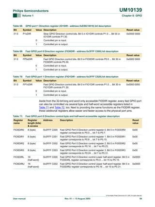
![UM10139
Philips Semiconductors
Volume 1
Chapter 8: GPIO
8.5 GPIO usage notes
8.5.1 Example 1: sequential accesses to IOSET and IOCLR affecting the
same GPIO pin/bit
State of the output configured GPIO pin is determined by writes into the pin’s port IOSET
and IOCLR registers. Last of these accesses to the IOSET/IOCLR register will determine
the final output of a pin.
In case of a code:
IO0DIR
IO0CLR
IO0SET
IO0CLR
=
=
=
=
0x0000
0x0000
0x0000
0x0000
0080
0080
0080
0080
;pin P0.7 configured as output
;P0.7 goes LOW
;P0.7 goes HIGH
;P0.7 goes LOW
pin P0.7 is configured as an output (write to IO0DIR register). After this, P0.7 output is set
to low (first write to IO0CLR register). Short high pulse follows on P0.7 (write access to
IO0SET), and the final write to IO0CLR register sets pin P0.7 back to low level.
8.5.2 Example 2: an immediate output of 0s and 1s on a GPIO port
Write access to port’s IOSET followed by write to the IOCLR register results with pins
outputting 0s being slightly later then pins outputting 1s. There are systems that can
tolerate this delay of a valid output, but for some applications simultaneous output of a
binary content (mixed 0s and 1s) within a group of pins on a single GPIO port is required.
This can be accomplished by writing to the port’s IOPIN register.
Following code will preserve existing output on PORT0 pins P0.[31:16] and P0.[7:0] and at
the same time set P0.[15:8] to 0xA5, regardless of the previous value of pins P0.[15:8]:
IO0PIN = (IO0PIN && 0xFFFF00FF) || 0x0000A500
The same outcome can be obtained using the fast port access.
Solution 1: using 32-bit (word) accessible fast GPIO registers
FIO0MASK = 0xFFFF00FF;
FIO0PIN = 0x0000A500;
Solution 2: using 16-bit (half-word) accessible fast GPIO registers
FIO0MASKL = 0x00FF;
FIO0PINL = 0xA500;
Solution 3: using 8-bit (byte) accessible fast GPIO registers
FIO0PIN1 = 0xA5;
© Koninklijke Philips Electronics N.V. 2005. All rights reserved.
User manual
Rev. 01 — 15 August 2005
92](https://image.slidesharecdn.com/armusrmanl-131212220701-phpapp02/85/Arm-usr-m-anl-92-320.jpg)
![UM10139
Philips Semiconductors
Volume 1
Chapter 8: GPIO
8.5.3 Writing to IOSET/IOCLR .vs. IOPIN
Write to the IOSET/IOCLR register allows easy change of the port’s selected output pin(s)
to high/low level at a time. Only pin/bit(s) in the IOSET/IOCLR written with 1 will be set to
high/low level, while those written as 0 will remain unaffected. However, by just writing to
either IOSET or IOCLR register it is not possible to instantaneously output arbitrary binary
data containing mixture of 0s and 1s on a GPIO port.
Write to the IOPIN register enables instantaneous output of a desired content on the
parallel GPIO. Binary data written into the IOPIN register will affect all output configured
pins of that parallel port: 0s in the IOPIN will produce low level pin outputs and 1s in IOPIN
will produce high level pin outputs. In order to change output of only a group of port’s pins,
application must logically AND readout from the IOPIN with mask containing 0s in bits
corresponding to pins that will be changed, and 1s for all others. Finally, this result has to
be logically ORred with the desired content and stored back into the IOPIN register.
Example 2 from above illustrates output of 0xA5 on PORT0 pins 15 to 8 while preserving
all other PORT0 output pins as they were before.
8.5.4 Output signal frequency considerations when using the legacy and
enhanced GPIO registers
The enhanced features of the fast GPIO ports available on this microcontroller make
GPIO pins more responsive to the code that has task of controlling them. In particular,
software access to a GPIO pin is 3.5 times faster via the fast GPIO registers than it is
when the legacy set of registers is used. As a result of the access speed increase, the
maximum output frequency of the digital pin is increased 3.5 times, too. This tremendous
increase of the output frequency is not always that visible when a plain C code is used,
and a portion of an application handling the fast port output might have to be written in an
assembly code and executed in the ARM mode.
Here is a code where the pin control section is written in assembly language for ARM. It
illustrates the difference between the fast and slow GPIO port output capabilities. Once
this code is compiled in the ARM mode, its execution from the on-chip Flash will yield the
best results when the MAM module is configured as described in Section 4.9 “MAM usage
notes” on page 49. Execution from the on-chip SRAM is independent from the MAM
setup.
ldr r0,=0xe01fc1a0 /*register address--enable fast port*/
mov r1,#0x1
str r1,[r0]
/*enable fast port0*/
ldr r1,=0xffffffff
ldr r0,=0x3fffc000 /*direction of fast port0*/
str r1,[r0]
ldr r0,=0xe0028018 /*direction of slow port 1*/
str r1,[r0]
ldr r0,=0x3fffc018 /*FIO0SET -- fast port0 register*/
ldr r1,=0x3fffc01c /*FIO0CLR0 -- fast port0 register*/
ldr r2,=0xC0010000 /*select fast port 0.16 for toggle*/
ldr r3,=0xE0028014 /*IO1SET -- slow port1 register*/
ldr r4,=0xE002801C /*IO1CLR -- slow port1 register*/
ldr r5,=0x00100000 /*select slow port 1.20 for toggle*/
/*Generate 2 pulses on the fast port*/
str r2,[r0]
© Koninklijke Philips Electronics N.V. 2005. All rights reserved.
User manual
Rev. 01 — 15 August 2005
93](https://image.slidesharecdn.com/armusrmanl-131212220701-phpapp02/85/Arm-usr-m-anl-93-320.jpg)
![UM10139
Philips Semiconductors
Volume 1
Chapter 8: GPIO
str r2,[r1]
str r2,[r0]
str r2,[r1]
/*Generate 2 pulses on the slow port*/
str r5,[r3]
str r5,[r4]
str r5,[r3]
str r5,[r4]
loop: b
loop
Figure 17 illustrates the code from above executed from the LPC2148 Flash memory. The
PLL generated FCCLK =60 MHz out of external FOSC = 12 MHz. The MAM was fully
enabled with MEMCR = 2 and MEMTIM = 3, and VPBDIV = 1 (PCLK = CCLK).
Fig 17. Illustration of the fast and slow GPIO access and output showing 3.5 x increase of the pin output
frequency
© Koninklijke Philips Electronics N.V. 2005. All rights reserved.
User manual
Rev. 01 — 15 August 2005
94](https://image.slidesharecdn.com/armusrmanl-131212220701-phpapp02/85/Arm-usr-m-anl-94-320.jpg)
![UM10139
Chapter 9: Universal Asynchronous Receiver/Transmitter 0
(UART0)
Rev. 01 — 15 August 2005
User manual
9.1 Features
•
•
•
•
•
16 byte Receive and Transmit FIFOs
Register locations conform to ‘550 industry standard.
Receiver FIFO trigger points at 1, 4, 8, and 14 bytes.
Built-in fractional baud rate generator with autobauding capabilities.
Mechanism that enables software and hardware flow control implementation.
9.2 Pin description
Table 95:
UART0 pin description
Pin
Type
Description
RXD0
Input
Serial Input. Serial receive data.
TXD0
Output
Serial Output. Serial transmit data.
9.3 Register description
UART0 contains registers organized as shown in Table 96. The Divisor Latch Access Bit
(DLAB) is contained in U0LCR[7] and enables access to the Divisor Latches.
© Koninklijke Philips Electronics N.V. 2005. All rights reserved.
User manual
Rev. 01 — 15 August 2005
95](https://image.slidesharecdn.com/armusrmanl-131212220701-phpapp02/85/Arm-usr-m-anl-95-320.jpg)
![xxxxxxxxxxxxxxxxxxxxx xxxxxxxxxxxxxxxxxxxxxxxxxx xxxxxxx x x x xxxxxxxxxxxxxxxxxxxxxxxxxxxxxx xxxxxxxxxxxxxxxxxxx xx xx xxxxx
xxxxxxxxxxxxxxxxxxxxxxxxxxx xxxxxxxxxxxxxxxxxxx xxxxxx xxxxxxxxxxxxxxxxxxxxxxxxxxxxxxxxxxx xxxxxxxxxxxx x x
xxxxxxxxxxxxxxxxxxxxx xxxxxxxxxxxxxxxxxxxxxxxxxxxxxx xxxxx xxxxxxxxxxxxxxxxxxxxxxxxxxxxxxxxxxxxxxxxxxxxxxxxxx xxxxxxxx
xxxxxxxxxxxxxxxxxxxxxxxxx xxxxxxxxxxxxxxxxxxxx xxx
Description
Bit functions and addresses
MSB
BIT7
LSB
BIT6
BIT5
BIT4
BIT3
BIT2
BIT1
Access Reset
Address
value[1]
BIT0
Receiver Buffer
Register
8-bit Read Data
RO
NA
0xE000 C000
(DLAB=0)
U0THR
Transmit Holding
Register
8-bit Write Data
WO
NA
0xE000 C000
(DLAB=0)
U0DLL
Divisor Latch LSB
8-bit Data
R/W
0x01
0xE000 C000
(DLAB=1)
U0DLM
Divisor Latch MSB
8-bit Data
R/W
0x00
0xE000 C004
(DLAB=1)
U0IER
Interrupt Enable
Register
-
-
-
-
-
En.ABTO En.ABEO R/W
0x00
-
-
-
-
-
0xE000 C004
(DLAB=0)
Interrupt ID Reg.
-
-
-
-
-
-
0x01
0xE000 C008
FIFOs Enabled
Rev. 01 — 15 August 2005
U0RBR
-
-
IIR3
IIR2
IIR1
IIR0
RX Trigger
-
-
-
TX FIFO
Reset
RX FIFO
Reset
FIFO
Enable
WO
0x00
0xE000 C008
Word Length Select R/W
0x00
0xE000 C00C
RO
0x60
0xE000 C014
R/W
0x00
0xE000 C01C
R/W
0x00
0xE000 C020
0x10
0xE000 C028
0x80
0xE000 C030
Philips Semiconductors
Name
UART0 register map
Volume 1
User manual
Table 96:
U0IIR
-
En.RX
Enable
En.RX
Lin.St.Int THRE Int Dat.Av.Int
ABTO Int ABEO Int RO
FIFO Control
Register
U0LCR
Line Control
Register
DLAB
Set
Break
Stick
Parity
Even
Par.Selct.
Parity
Enable
No. of
Stop Bits
U0LSR
Line Status
Register
RX FIFO
Error
TEMT
THRE
BI
FE
PE
U0SCR
Scratch Pad Reg.
U0ACR
Auto-baud Control
Register
U0FDR
Fractional Divider
Register
[1]
-
-
-
-
-
-
-
-
ABTO
Int.Clr
ABEO
Int.Clr
-
-
Aut.Rstrt.
Mode
Start
Reserved[31:8]
MulVal
TXEN
-
DivAddVal
-
-
-
-
-
Reset value reflects the data stored in used bits only. It does not include reserved bits content.
-
R/W
UM10139
TX. Enable Reg.
DR
8-bit Data
-
U0TER
OE
Chapter 9: UART0
96
© Koninklijke Philips Electronics N.V. 2005. All rights reserved.
U0FCR](https://image.slidesharecdn.com/armusrmanl-131212220701-phpapp02/85/Arm-usr-m-anl-96-320.jpg)

![UM10139
Philips Semiconductors
Volume 1
Chapter 9: UART0
If the U0FDR register value does not comply to these two requests then the fractional
divider output is undefined. If DIVADDVAL is zero then the fractional divider is disabled
and the clock will not be divided.
The value of the U0FDR should not be modified while transmitting/receiving data or data
may be lost or corrupted.
Usage Note: For practical purposes, UART0 baudrate formula can be written in a way
that identifies the part of a UART baudrate generated without the fractional baudrate
generator, and the correction factor that this module adds:
(2)
PCLK
MulVal
UART0 baudrate = ---------------------------------------------------------------------------- × ----------------------------------------------------------16 × ( 16 × U0DLM + U0DLL ) ( MulVal + DivAddVal )
Based on this representation, fractional baudrate generator contribution can also be
described as a prescaling with a factor of MULVAL / (MULVAL + DIVADDVAL).
9.3.5 UART0 baudrate calculation
Example 1: Using UART0baudrate formula from above, it can be determined that system
with PCLK = 20 MHz, U0DL = 130 (U0DLM = 0x00 and U0DLL = 0x82), DIVADDVAL = 0
and MULVAL = 1 will enable UART0 with UART0baudrate = 9615 bauds.
Example 2: Using UART0baudrate formula from above, it can be determined that system
with PCLK = 20 MHz, U0DL = 93 (U0DLM = 0x00 and U0DLL = 0x5D), DIVADDVAL = 2
and MULVAL = 5 will enable UART0 with UART0baudrate = 9600 bauds.
Table 102: Baudrates available when using 20 MHz peripheral clock (PCLK = 20 MHz)
Desired
baudrate
MULVAL = 0 DIVADDVAL = 0
U0DLM:U0DLL
% error[3]
Optimal MULVAL & DIVADDVAL
U0DLM:U0DLL
dec[1]
Fractional
pre-scaler value
% error[3]
hex[2]
dec[1]
50
61A8
25000
0.0000
25000
1/(1+0)
0.0000
75
411B
16667
0.0020
12500
3/(3+1)
0.0000
110
2C64
11364
0.0032
6250
11/(11+9)
0.0000
134.5
244E
9294
0.0034
3983
3/(3+4)
0.0001
150
208D
8333
0.0040
6250
3/(3+1)
0.0000
300
1047
4167
0.0080
3125
3/(3+1)
0.0000
600
0823
2083
0.0160
1250
3/(3+2)
0.0000
1200
0412
1042
0.0320
625
3/(3+2)
0.0000
1800
02B6
694
0.0640
625
9/(9+1)
0.0000
2000
0271
625
0.0000
625
1/(1+0)
0.0000
2400
0209
521
0.0320
250
12/(12+13)
0.0000
3600
015B
347
0.0640
248
5/(5+2)
0.0064
4800
0104
260
0.1600
125
12/(12+13)
0.0000
MULDIV
MULDIV + DIVADDVAL
© Koninklijke Philips Electronics N.V. 2005. All rights reserved.
User manual
Rev. 01 — 15 August 2005
99](https://image.slidesharecdn.com/armusrmanl-131212220701-phpapp02/85/Arm-usr-m-anl-99-320.jpg)
![UM10139
Philips Semiconductors
Volume 1
Chapter 9: UART0
Table 102: Baudrates available when using 20 MHz peripheral clock (PCLK = 20 MHz)
Desired
baudrate
MULVAL = 0 DIVADDVAL = 0
U0DLM:U0DLL
% error[3]
Optimal MULVAL & DIVADDVAL
U0DLM:U0DLL
dec[1]
Fractional
pre-scaler value
% error[3]
hex[2]
dec[1]
7200
00AE
174
0.2240
124
5/(5+2)
0.0064
9600
0082
130
0.1600
93
5/(5+2)
0.0064
19200
0041
65
0.1600
31
10/(10+11)
0.0064
38400
0021
33
1.3760
12
7/(7+12)
0.0594
56000
0021
22
1.4400
13
7/(7+5)
0.0160
57600
0016
22
1.3760
19
7/(7+1)
0.0594
112000
000B
11
1.4400
6
7/(7+6)
0.1600
115200
000B
11
1.3760
4
7/(7+12)
0.0594
224000
0006
6
7.5200
3
7/(7+6)
0.1600
448000
0003
3
7.5200
2
5/(5+2)
0.3520
MULDIV
MULDIV + DIVADDVAL
[1]
Values in the row represent decimal equivalent of a 16 bit long content (DLM:DLL).
[2]
Values in the row represent hex equivalent of a 16 bit long content (DLM:DLL).
[3]
Refers to the percent error between desired and actual baudrate.
9.3.6 UART0 Interrupt Enable Register (U0IER - 0xE000 C004, when
DLAB = 0)
The U0IER is used to enable UART0 interrupt sources.
Table 103: UART0 Interrupt Enable Register (U0IER - address 0xE000 C004, when DLAB = 0)
bit description
Bit
Symbol
0
Value
RBR
Interrupt
Enable
Description
Reset
value
U0IER[0] enables the Receive Data Available interrupt
for UART0. It also controls the Character Receive
Time-out interrupt.
0
0
1
1
THRE
Interrupt
Enable
Disable the RDA interrupts.
Enable the RDA interrupts.
U0IER[1] enables the THRE interrupt for UART0. The
status of this can be read from U0LSR[5].
7:4
RX Line
Status
Interrupt
Enable
-
Disable the THRE interrupts.
1
2
0
0
Enable the THRE interrupts.
U0IER[2] enables the UART0 RX line status interrupts.
0
The status of this interrupt can be read from U0LSR[4:1].
0
Disable the RX line status interrupts.
1
Enable the RX line status interrupts.
-
Reserved, user software should not write ones to
reserved bits. The value read from a reserved bit is not
defined.
NA
© Koninklijke Philips Electronics N.V. 2005. All rights reserved.
User manual
Rev. 01 — 15 August 2005
100](https://image.slidesharecdn.com/armusrmanl-131212220701-phpapp02/85/Arm-usr-m-anl-100-320.jpg)
![UM10139
Philips Semiconductors
Volume 1
Chapter 9: UART0
Table 103: UART0 Interrupt Enable Register (U0IER - address 0xE000 C004, when DLAB = 0)
bit description
Bit
Symbol
8
Value
ABTOIntEn
Description
Reset
value
U1IER8 enables the auto-baud time-out interrupt.
0
0
1
9
Disable Auto-baud Time-out Interrupt.
Enable Auto-baud Time-out Interrupt.
ABEOIntEn
U1IER9 enables the end of auto-baud interrupt.
0
1
31:10
-
Enable End of Auto-baud Interrupt.
-
Reserved, user software should not write ones to
reserved bits. The value read from a reserved bit is not
defined.
0
Disable End of Auto-baud Interrupt.
NA
9.3.7 UART0 Interrupt Identification Register (U0IIR - 0xE000 C008, Read
Only)
The U0IIR provides a status code that denotes the priority and source of a pending
interrupt. The interrupts are frozen during an U0IIR access. If an interrupt occurs during
an U0IIR access, the interrupt is recorded for the next U0IIR access.
Table 104: UART0 Interrupt Identification Register (UOIIR - address 0xE000 C008, read only)
bit description
Bit
Symbol
0
Value Description
Interrupt
Pending
Note that U0IIR[0] is active low. The pending interrupt can
be determined by evaluating U0IIR[3:1].
0
1
At least one interrupt is pending.
1
3:1
Reset
value
No pending interrupts.
Interrupt
Identification
U0IER[3:1] identifies an interrupt corresponding to the
UART0 Rx FIFO. All other combinations of U0IER[3:1] not
listed above are reserved (000,100,101,111).
011
1 - Receive Line Status (RLS).
010
2a - Receive Data Available (RDA).
110
2b - Character Time-out Indicator (CTI).
001
0
3 - THRE Interrupt
5:4
-
Reserved, user software should not write ones to reserved
bits. The value read from a reserved bit is not defined.
NA
7:6
FIFO Enable
These bits are equivalent to U0FCR[0].
0
8
ABEOInt
End of auto-baud interrupt. True if auto-baud has finished
successfully and interrupt is enabled.
0
9
ABTOInt
Auto-baud time-out interrupt. True if auto-baud has timed
out and interrupt is enabled.
0
Reserved, user software should not write ones to reserved
bits. The value read from a reserved bit is not defined.
NA
31:10 -
Interrupts are handled as described in Table 105. Given the status of U0IIR[3:0], an
interrupt handler routine can determine the cause of the interrupt and how to clear the
active interrupt. The U0IIR must be read in order to clear the interrupt prior to exiting the
Interrupt Service Routine.
© Koninklijke Philips Electronics N.V. 2005. All rights reserved.
User manual
Rev. 01 — 15 August 2005
101](https://image.slidesharecdn.com/armusrmanl-131212220701-phpapp02/85/Arm-usr-m-anl-101-320.jpg)
![UM10139
Philips Semiconductors
Volume 1
Chapter 9: UART0
The UART0 RLS interrupt (U0IIR[3:1] = 011) is the highest priority interrupt and is set
whenever any one of four error conditions occur on the UART0 Rx input: overrun error
(OE), parity error (PE), framing error (FE) and break interrupt (BI). The UART0 Rx error
condition that set the interrupt can be observed via U0LSR[4:1]. The interrupt is cleared
upon an U0LSR read.
The UART0 RDA interrupt (U0IIR[3:1] = 010) shares the second level priority with the CTI
interrupt (U0IIR[3:1] = 110). The RDA is activated when the UART0 Rx FIFO reaches the
trigger level defined in U0FCR[7:6] and is reset when the UART0 Rx FIFO depth falls
below the trigger level. When the RDA interrupt goes active, the CPU can read a block of
data defined by the trigger level.
The CTI interrupt (U0IIR[3:1] = 110) is a second level interrupt and is set when the UART0
Rx FIFO contains at least one character and no UART0 Rx FIFO activity has occurred in
3.5 to 4.5 character times. Any UART0 Rx FIFO activity (read or write of UART0 RSR) will
clear the interrupt. This interrupt is intended to flush the UART0 RBR after a message has
been received that is not a multiple of the trigger level size. For example, if a peripheral
wished to send a 105 character message and the trigger level was 10 characters, the CPU
would receive 10 RDA interrupts resulting in the transfer of 100 characters and 1 to 5 CTI
interrupts (depending on the service routine) resulting in the transfer of the remaining 5
characters.
Table 105: UART0 interrupt handling
U0IIR[3:0] Priority Interrupt Type
value[1]
Interrupt Source
0001
None
None
-
Interrupt Reset
-
0110
Highest
RX Line Status / Error
OE[2]
0100
Second
RX Data Available
Rx data available or trigger level reached in FIFO
(U0FCR0=1)
U0RBR Read[3] or
UART0 FIFO drops
below trigger level
1100
Second
Character Time-out
indication
Minimum of one character in the Rx FIFO and no
character input or removed during a time period
depending on how many characters are in FIFO
and what the trigger level is set at (3.5 to 4.5
character times).
U0RBR Read[3]
or
PE[2]
or
FE[2]
or
BI[2]
U0LSR Read[2]
The exact time will be:
[(word length) × 7 − 2] × 8 + [(trigger level −
number of characters) × 8 + 1] RCLKs
0010
Third
THRE
THRE[2]
U0IIR Read (if source of
interrupt) or THR write[4]
[1]
Values "0000", “0011”, “0101”, “0111”, “1000”, “1001”, “1010”, “1011”,”1101”,”1110”,”1111” are reserved.
[2]
For details see Section 9.3.10 “UART0 Line Status Register (U0LSR - 0xE000 C014, Read Only)”
[3]
For details see Section 9.3.1 “UART0 Receiver Buffer Register (U0RBR - 0xE000 C000, when DLAB = 0,
Read Only)”
[4]
For details see Section 9.3.7 “UART0 Interrupt Identification Register (U0IIR - 0xE000 C008, Read Only)”
and Section 9.3.2 “UART0 Transmit Holding Register (U0THR - 0xE000 C000, when DLAB = 0, Write
Only)”
The UART0 THRE interrupt (U0IIR[3:1] = 001) is a third level interrupt and is activated
when the UART0 THR FIFO is empty provided certain initialization conditions have been
met. These initialization conditions are intended to give the UART0 THR FIFO a chance to
fill up with data to eliminate many THRE interrupts from occurring at system start-up. The
© Koninklijke Philips Electronics N.V. 2005. All rights reserved.
User manual
Rev. 01 — 15 August 2005
102](https://image.slidesharecdn.com/armusrmanl-131212220701-phpapp02/85/Arm-usr-m-anl-102-320.jpg)
![UM10139
Philips Semiconductors
Volume 1
Chapter 9: UART0
initialization conditions implement a one character delay minus the stop bit whenever
THRE=1 and there have not been at least two characters in the U0THR at one time since
the last THRE = 1 event. This delay is provided to give the CPU time to write data to
U0THR without a THRE interrupt to decode and service. A THRE interrupt is set
immediately if the UART0 THR FIFO has held two or more characters at one time and
currently, the U0THR is empty. The THRE interrupt is reset when a U0THR write occurs or
a read of the U0IIR occurs and the THRE is the highest interrupt (U0IIR[3:1] = 001).
9.3.8 UART0 FIFO Control Register (U0FCR - 0xE000 C008)
The U0FCR controls the operation of the UART0 Rx and TX FIFOs.
Table 106: UART0 FIFO Control Register (U0FCR - address 0xE000 C008) bit description
Bit
Symbol
Value
0
FIFO Enable 0
Description
Reset value
UART0 FIFOs are disabled. Must not be used in the 0
application.
1
Active high enable for both UART0 Rx and TX
FIFOs and U0FCR[7:1] access. This bit must be set
for proper UART0 operation. Any transition on this
bit will automatically clear the UART0 FIFOs.
RX FIFO
Reset
0
No impact on either of UART0 FIFOs.
1
Writing a logic 1 to U0FCR[1] will clear all bytes in
UART0 Rx FIFO and reset the pointer logic. This bit
is self-clearing.
TX FIFO
Reset
0
No impact on either of UART0 FIFOs.
1
Writing a logic 1 to U0FCR[2] will clear all bytes in
UART0 TX FIFO and reset the pointer logic. This bit
is self-clearing.
5:3
-
0
Reserved, user software should not write ones to
reserved bits. The value read from a reserved bit is
not defined.
NA
7:6
RX Trigger
Level
These two bits determine how many receiver
UART0 FIFO characters must be written before an
interrupt is activated.
0
1
2
00
0
0
Trigger level 0 (1 character or 0x01)
01
Trigger level 1 (4 characters or 0x04)
10
Trigger level 2 (8 characters or 0x08)
11
Trigger level 3 (14 characters or 0x0E)
9.3.9 UART0 Line Control Register (U0LCR - 0xE000 C00C)
The U0LCR determines the format of the data character that is to be transmitted or
received.
Table 107: UART0 Line Control Register (U0LCR - address 0xE000 C00C) bit description
Bit
Symbol
Value
Description
Reset value
1:0
Word Length
Select
00
5 bit character length
0
01
6 bit character length
10
7 bit character length
11
8 bit character length
© Koninklijke Philips Electronics N.V. 2005. All rights reserved.
User manual
Rev. 01 — 15 August 2005
103](https://image.slidesharecdn.com/armusrmanl-131212220701-phpapp02/85/Arm-usr-m-anl-103-320.jpg)
![UM10139
Philips Semiconductors
Volume 1
Chapter 9: UART0
Table 107: UART0 Line Control Register (U0LCR - address 0xE000 C00C) bit description
Bit
Symbol
Value
Description
Reset value
2
Stop Bit Select
0
1 stop bit.
0
1
2 stop bits (1.5 if U0LCR[1:0]=00).
0
Disable parity generation and checking.
1
Enable parity generation and checking.
00
Odd parity. Number of 1s in the transmitted character and the
attached parity bit will be odd.
01
Even Parity. Number of 1s in the transmitted character and the
attached parity bit will be even.
10
Forced "1" stick parity.
11
Forced "0" stick parity.
0
Disable break transmission.
1
Enable break transmission. Output pin UART0 TXD is forced to
logic 0 when U0LCR[6] is active high.
3
5:4
6
7
Parity Enable
Parity Select
Break Control
Divisor Latch
0
Access Bit (DLAB) 1
0
0
0
Disable access to Divisor Latches.
0
Enable access to Divisor Latches.
9.3.10 UART0 Line Status Register (U0LSR - 0xE000 C014, Read Only)
The U0LSR is a read-only register that provides status information on the UART0 TX and
RX blocks.
Table 108: UART0 Line Status Register (U0LSR - address 0xE000 C014, read only) bit description
Bit Symbol
0
Receiver Data
Ready
(RDR)
Value Description
Reset value
U0LSR0 is set when the U0RBR holds an unread character and is cleared
when the UART0 RBR FIFO is empty.
U0RBR is empty.
1
1
0
U0RBR contains valid data.
Overrun Error
(OE)
The overrun error condition is set as soon as it occurs. An U0LSR read clears 0
U0LSR1. U0LSR1 is set when UART0 RSR has a new character assembled
and the UART0 RBR FIFO is full. In this case, the UART0 RBR FIFO will not
be overwritten and the character in the UART0 RSR will be lost.
0
Overrun error status is inactive.
1
2
0
Overrun error status is active.
Parity Error
(PE)
When the parity bit of a received character is in the wrong state, a parity error 0
occurs. An U0LSR read clears U0LSR[2]. Time of parity error detection is
dependent on U0FCR[0].
Note: A parity error is associated with the character at the top of the UART0
RBR FIFO.
0
Parity error status is inactive.
1
Parity error status is active.
© Koninklijke Philips Electronics N.V. 2005. All rights reserved.
User manual
Rev. 01 — 15 August 2005
104](https://image.slidesharecdn.com/armusrmanl-131212220701-phpapp02/85/Arm-usr-m-anl-104-320.jpg)
![UM10139
Philips Semiconductors
Volume 1
Chapter 9: UART0
Table 108: UART0 Line Status Register (U0LSR - address 0xE000 C014, read only) bit description
Bit Symbol
3
Value Description
Framing Error
(FE)
Reset value
When the stop bit of a received character is a logic 0, a framing error occurs. 0
An U0LSR read clears U0LSR[3]. The time of the framing error detection is
dependent on U0FCR0. Upon detection of a framing error, the Rx will attempt
to resynchronize to the data and assume that the bad stop bit is actually an
early start bit. However, it cannot be assumed that the next received byte will
be correct even if there is no Framing Error.
Note: A framing error is associated with the character at the top of the UART0
RBR FIFO.
0
1
4
Framing error status is inactive.
Framing error status is active.
Break Interrupt
(BI)
When RXD0 is held in the spacing state (all 0’s) for one full character
0
transmission (start, data, parity, stop), a break interrupt occurs. Once the
break condition has been detected, the receiver goes idle until RXD0 goes to
marking state (all 1’s). An U0LSR read clears this status bit. The time of break
detection is dependent on U0FCR[0].
Note: The break interrupt is associated with the character at the top of the
UART0 RBR FIFO.
0
1
5
6
Transmitter
Holding
Register Empty
(THRE))
Transmitter
Empty
(TEMT)
Break interrupt status is inactive.
Break interrupt status is active.
THRE is set immediately upon detection of an empty UART0 THR and is
cleared on a U0THR write.
0
U0THR contains valid data.
1
U0THR is empty.
TEMT is set when both U0THR and U0TSR are empty; TEMT is cleared when 1
either the U0TSR or the U0THR contain valid data.
0
U0THR and/or the U0TSR contains valid data.
1
7
1
U0THR and the U0TSR are empty.
Error in RX
FIFO
(RXFE)
U0LSR[7] is set when a character with a Rx error such as framing error, parity 0
error or break interrupt, is loaded into the U0RBR. This bit is cleared when the
U0LSR register is read and there are no subsequent errors in the UART0
FIFO.
0
U0RBR contains no UART0 RX errors or U0FCR[0]=0.
1
UART0 RBR contains at least one UART0 RX error.
9.3.11 UART0 Scratch pad register (U0SCR - 0xE000 C01C)
The U0SCR has no effect on the UART0 operation. This register can be written and/or
read at user’s discretion. There is no provision in the interrupt interface that would indicate
to the host that a read or write of the U0SCR has occurred.
Table 109: UART0 Scratch pad register (U0SCR - address 0xE000 C01C) bit description
Bit
Symbol
Description
Reset value
7:0
Pad
A readable, writable byte.
0x00
© Koninklijke Philips Electronics N.V. 2005. All rights reserved.
User manual
Rev. 01 — 15 August 2005
105](https://image.slidesharecdn.com/armusrmanl-131212220701-phpapp02/85/Arm-usr-m-anl-105-320.jpg)
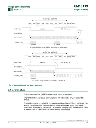
![UM10139
Philips Semiconductors
Volume 1
Chapter 9: UART0
U0TX
U0THR
NTXRDY
U0TSR
TXD0
U0BRG
U0DLL
NBAUDOUT
U0DLM
RCLK
U0RX
NRXRDY
INTERRUPT
U0RBR
U0INTR
U0RSR
RXD0
U0IER
U0IIR
U0FCR
U0LSR
U0SCR
U0LCR
PA[2:0]
PSEL
PSTB
PWRITE
VPB
INTERFACE
PD[7:0]
DDIS
AR
MR
PCLK
Fig 19. UART0 block diagram
© Koninklijke Philips Electronics N.V. 2005. All rights reserved.
User manual
Rev. 01 — 15 August 2005
111](https://image.slidesharecdn.com/armusrmanl-131212220701-phpapp02/85/Arm-usr-m-anl-111-320.jpg)
![UM10139
Chapter 10: Universal Asynchronous Receiver/Transmitter 1
(UART1)
Rev. 01 — 15 August 2005
User manual
10.1 Features
•
•
•
•
•
•
•
UART1 is identical to UART0, with the addition of a modem interface.
16 byte Receive and Transmit FIFOs.
Register locations conform to ‘550 industry standard.
Receiver FIFO trigger points at 1, 4, 8, and 14 bytes.
Built-in fractional baud rate generator with autobauding capabilities.
Mechanism that enables software and hardware flow control implementation.
Standard modem interface signals included with flow control (auto-CTS/RTS) fully
supported in hardware (LPC2144/6/8 only).
10.2 Pin description
Table 112: UART1 pin description
Pin
Type
Description
RXD1
Input
Serial Input. Serial receive data.
TXD1
Output
Serial Output. Serial transmit data.
CTS1[1]
Input
Clear To Send. Active low signal indicates if the external modem is ready to accept transmitted
data via TXD1 from the UART1. In normal operation of the modem interface (U1MCR[4] = 0), the
complement value of this signal is stored in U1MSR[4]. State change information is stored in
U1MSR[0] and is a source for a priority level 4 interrupt, if enabled (U1IER[3] = 1).
DCD1[1]
Input
Data Carrier Detect. Active low signal indicates if the external modem has established a
communication link with the UART1 and data may be exchanged. In normal operation of the
modem interface (U1MCR[4]=0), the complement value of this signal is stored in U1MSR[7]. State
change information is stored in U1MSR3 and is a source for a priority level 4 interrupt, if enabled
(U1IER[3] = 1).
DSR1[1]
Input
Data Set Ready. Active low signal indicates if the external modem is ready to establish a
communications link with the UART1. In normal operation of the modem interface (U1MCR[4] = 0),
the complement value of this signal is stored in U1MSR[5]. State change information is stored in
U1MSR[1] and is a source for a priority level 4 interrupt, if enabled (U1IER[3] = 1).
DTR1[1]
Output
Data Terminal Ready. Active low signal indicates that the UART1 is ready to establish connection
with external modem. The complement value of this signal is stored in U1MCR[0].
RI1[1]
Input
Ring Indicator. Active low signal indicates that a telephone ringing signal has been detected by
the modem. In normal operation of the modem interface (U1MCR[4] = 0), the complement value of
this signal is stored in U1MSR[6]. State change information is stored in U1MSR[2] and is a source
for a priority level 4 interrupt, if enabled (U1IER[3] = 1).
RTS1[1]
Output
Request To Send. Active low signal indicates that the UART1 would like to transmit data to the
external modem. The complement value of this signal is stored in U1MCR[1].
[1]
LPC2144/6/8 only.
© Koninklijke Philips Electronics N.V. 2005. All rights reserved.
User manual
Rev. 01 — 15 August 2005
112](https://image.slidesharecdn.com/armusrmanl-131212220701-phpapp02/85/Arm-usr-m-anl-112-320.jpg)
![UM10139
Philips Semiconductors
Volume 1
Chapter 10: UART1
10.3 Register description
UART1 contains registers organized as shown in Table 76. The Divisor Latch Access Bit
(DLAB) is contained in U1LCR[7] and enables access to the Divisor Latches.
© Koninklijke Philips Electronics N.V. 2005. All rights reserved.
User manual
Rev. 01 — 15 August 2005
113](https://image.slidesharecdn.com/armusrmanl-131212220701-phpapp02/85/Arm-usr-m-anl-113-320.jpg)
![xxxxxxxxxxxxxxxxxxxxx xxxxxxxxxxxxxxxxxxxxxxxxxx xxxxxxx x x x xxxxxxxxxxxxxxxxxxxxxxxxxxxxxx xxxxxxxxxxxxxxxxxxx xx xx xxxxx
xxxxxxxxxxxxxxxxxxxxxxxxxxx xxxxxxxxxxxxxxxxxxx xxxxxx xxxxxxxxxxxxxxxxxxxxxxxxxxxxxxxxxxx xxxxxxxxxxxx x x
xxxxxxxxxxxxxxxxxxxxx xxxxxxxxxxxxxxxxxxxxxxxxxxxxxx xxxxx xxxxxxxxxxxxxxxxxxxxxxxxxxxxxxxxxxxxxxxxxxxxxxxxxx xxxxxxxx
xxxxxxxxxxxxxxxxxxxxxxxxx xxxxxxxxxxxxxxxxxxxx xxx
Name
Description
Bit functions and addresses
BIT7
LSB
BIT6
BIT5
BIT4
BIT3
BIT2
BIT1
Address
BIT0
U1RBR
Receiver Buffer
Register
8-bit Read Data
RO
NA
0xE001 0000
(DLAB=0)
U1THR
Transmit Holding
Register
8-bit Write Data
WO
NA
0xE001 0000
(DLAB=0)
U1DLL
Divisor Latch LSB
8-bit Data
R/W
0x01
0xE001 0000
(DLAB=1)
U1DLM
Divisor Latch MSB
8-bit Data
R/W
0x00
0xE001 0004
(DLAB=1)
U1IER
Interrupt Enable
Register
En.ABTO En.ABEO R/W
0x00
0xE001 0004
(DLAB=0)
0x01
Volume 1
MSB
Access Reset
value[1]
Philips Semiconductors
User manual
Table 113: UART1 register map
0xE001 0008
Rev. 01 — 15 August 2005
-
-
En.CTS
Int[2]
-
-
-
-
-
-
-
-
-
-
-
IIR3
IIR2
IIR1
IIR0
RX Trigger
Interrupt ID Reg.
-
FIFOs Enabled
U1IIR
-
-
-
-
-
-
TX FIFO
Reset
RX FIFO
Reset
FIFO
Enable
WO
0x00
0xE001 0008
Word Length Select R/W
0x00
0xE001 000C
E.Modem En. RX
Enable
En. RX
St.Int[2] Lin.St. Int THRE Int Dat.Av.Int
ABTO Int ABEO Int RO
DLAB
Set
Break
Stick
Parity
Even
Par.Selct.
Parity
Enable
No. of
Stop Bits
U1MCR[2]
Modem Ctrl. Reg.
CTSen
RTSen
-
LoopBck.
-
-
RTS
DTR
R/W
0x00
0xE001 0010
U1LSR
Line Status
Register
RX FIFO
Error
TEMT
THRE
BI
FE
PE
OE
DR
RO
0x60
0xE001 0014
U1MSR[2]
Modem Status
Register
DCD
RI
DSR
CTS
Delta
DCD
Trailing
Edge RI
Delta
DSR
Delta
CTS
RO
0x00
0xE001 0018
U1SCR
Scratch Pad Reg.
R/W
0x00
0xE001 001C
U1ACR
Auto-baud Control
Register
-
-
-
-
-
-
ABTO
IntClr
ABEO
IntClr
R/W
0x00
0xE001 0020
-
-
-
-
-
Aut.Rstrt.
Mode
Start
R/W
0x10
0xE001 0028
R/W
0x80
0xE001 0030
U1FDR
U1TER
8-bit Data
Fractional Divider
Register
TX. Enable Reg.
Reserved[31:8]
MulVal
TXEN
-
DivAddVal
-
-
-
-
-
114
[1]
Reset value reflects the data stored in used bits only. It does not include reserved bits content.
[2]
Modem specific features are available in LPC2144/6/8 only.
-
UM10139
Line Control
Register
Chapter 10: UART1
FIFO Control
Register
U1LCR
© Koninklijke Philips Electronics N.V. 2005. All rights reserved.
U1FCR](https://image.slidesharecdn.com/armusrmanl-131212220701-phpapp02/85/Arm-usr-m-anl-114-320.jpg)
![UM10139
Philips Semiconductors
Volume 1
Chapter 10: UART1
If the U1FDR register value does not comply to these two requests then the fractional
divider output is undefined. If DIVADDVAL is zero then the fractional divider is disabled
and the clock will not be divided.
The value of the U1FDR should not be modified while transmitting/receiving data or data
may be lost or corrupted.
Usage Note: For practical purposes, UART1 baudrate formula can be written in a way
that identifies the part of a UART baudrate generated without the fractional baudrate
generator, and the correction factor that this module adds:
(5)
PCLK
MulVal
UART1 baudrate = ---------------------------------------------------------------------------- × ----------------------------------------------------------16 × ( 16 × U1DLM + U1DLL ) ( MulVal + DivAddVal )
Based on this representation, fractional baudrate generator contribution can also be
described as a prescaling with a factor of MULVAL / (MULVAL + DIVADDVAL).
10.3.5 UART1 baudrate calculation
Example 1: Using UART1baudrate formula from above, it can be determined that system
with PCLK = 20 MHz, U1DL = 130 (U1DLM = 0x00 and U1DLL = 0x82), DIVADDVAL = 0
and MULVAL = 1 will enable UART1 with UART1baudrate = 9615 bauds.
Example 2: Using UART1baudrate formula from above, it can be determined that system
with PCLK = 20 MHz, U1DL = 93 (U1DLM = 0x00 and U1DLL = 0x5D), DIVADDVAL = 2
and MULVAL = 5 will enable UART1 with UART1baudrate = 9600 bauds.
Table 119: Baudrates available when using 20 MHz peripheral clock (PCLK = 20 MHz)
Desired
baudrate
MULVAL = 0 DIVADDVAL = 0
U1DLM:U1DLL
% error[3]
Optimal MULVAL & DIVADDVAL
U1DLM:U1DLL
dec[1]
Fractional
pre-scaler value
% error[3]
hex[2]
dec[1]
50
61A8
25000
0.0000
25000
1/(1+0)
0.0000
75
411B
16667
0.0020
12500
3/(3+1)
0.0000
110
2C64
11364
0.0032
6250
11/(11+9)
0.0000
134.5
244E
9294
0.0034
3983
3/(3+4)
0.0001
150
208D
8333
0.0040
6250
3/(3+1)
0.0000
300
1047
4167
0.0080
3125
3/(3+1)
0.0000
600
0823
2083
0.0160
1250
3/(3+2)
0.0000
1200
0412
1042
0.0320
625
3/(3+2)
0.0000
1800
02B6
694
0.0640
625
9/(9+1)
0.0000
2000
0271
625
0.0000
625
1/(1+0)
0.0000
2400
0209
521
0.0320
250
12/(12+13)
0.0000
3600
015B
347
0.0640
248
5/(5+2)
0.0064
4800
0104
260
0.1600
125
12/(12+13)
0.0000
MULDIV
MULDIV + DIVADDVAL
© Koninklijke Philips Electronics N.V. 2005. All rights reserved.
User manual
Rev. 01 — 15 August 2005
117](https://image.slidesharecdn.com/armusrmanl-131212220701-phpapp02/85/Arm-usr-m-anl-117-320.jpg)
![UM10139
Philips Semiconductors
Volume 1
Chapter 10: UART1
Table 119: Baudrates available when using 20 MHz peripheral clock (PCLK = 20 MHz)
Desired
baudrate
MULVAL = 0 DIVADDVAL = 0
U1DLM:U1DLL
% error[3]
Optimal MULVAL & DIVADDVAL
U1DLM:U1DLL
dec[1]
% error[3]
Fractional
pre-scaler value
hex[2]
dec[1]
7200
00AE
174
0.2240
124
5/(5+2)
0.0064
9600
0082
130
0.1600
93
5/(5+2)
0.0064
19200
0041
65
0.1600
31
10/(10+11)
0.0064
38400
0021
33
1.3760
12
7/(7+12)
0.0594
56000
0021
22
1.4400
13
7/(7+5)
0.0160
57600
0016
22
1.3760
19
7/(7+1)
0.0594
112000
000B
11
1.4400
6
7/(7+6)
0.1600
115200
000B
11
1.3760
4
7/(7+12)
0.0594
224000
0006
6
7.5200
3
7/(7+6)
0.1600
448000
0003
3
7.5200
2
5/(5+2)
0.3520
MULDIV
MULDIV + DIVADDVAL
[1]
Values in the row represent decimal equivalent of a 16 bit long content (DLM:DLL).
[2]
Values in the row represent hex equivalent of a 16 bit long content (DLM:DLL).
[3]
Refers to the percent error between desired and actual baudrate.
10.3.6 UART1 Interrupt Enable Register (U1IER - 0xE001 0004, when
DLAB = 0)
The U1IER is used to enable UART1 interrupt sources.
Table 120: UART1 Interrupt Enable Register (U1IER - address 0xE001 0004, when DLAB = 0)
bit description
Bit
Symbol
0
RBR
Interrupt
Enable
Value
Description
Reset value
U1IER[0] enables the Receive Data Available
interrupt for UART1. It also controls the Character
Receive Time-out interrupt.
0
0
1
Disable the RDA interrupts.
1
Enable the RDA interrupts.
THRE
Interrupt
Enable
U1IER[1] enables the THRE interrupt for UART1.
The status of this interrupt can be read from
U1LSR[5].
0
2
Disable the THRE interrupts.
1
Enable the THRE interrupts.
RX Line
Interrupt
Enable
U1IER[2] enables the UART1 RX line status
interrupts. The status of this interrupt can be read
from U1LSR[4:1].
0
Modem
Status
Interrupt
Enable[1]
0
Disable the RX line status interrupts.
1
3
0
Enable the RX line status interrupts.
U1IER[3] enables the modem interrupt. The status
of this interrupt can be read from U1MSR[3:0].
0
Disable the modem interrupt.
1
0
Enable the modem interrupt.
© Koninklijke Philips Electronics N.V. 2005. All rights reserved.
User manual
Rev. 01 — 15 August 2005
118](https://image.slidesharecdn.com/armusrmanl-131212220701-phpapp02/85/Arm-usr-m-anl-118-320.jpg)
![UM10139
Philips Semiconductors
Volume 1
Chapter 10: UART1
Table 120: UART1 Interrupt Enable Register (U1IER - address 0xE001 0004, when DLAB = 0)
bit description
Bit
Symbol
6:4
-
7
Value
CTS
Interrupt
Enable[1]
-
Description
Reset value
Reserved, user software should not write ones to
reserved bits. The value read from a reserved bit is
not defined.
NA
If auto-CTS mode is enabled this bit
0
enables/disables the modem status interrupt
generation on a CTS1 signal transition. If auto-CTS
mode is disabled a CTS1 transition will generate an
interrupt if Modem Status Interrupt Enable
(U1IER[3]) is set.
In normal operation a CTS1 signal transition will
generate a Modem Status Interrupt unless the
interrupt has been disabled by clearing the
U1IER[3] bit in the U1IER register. In auto-CTS
mode a transition on the CTS1 bit will trigger an
interrupt only if both the U1IER[3] and U1IER[7] bits
are set.
0
8
Disable the CTS interrupt.
1
Enable the CTS interrupt.
ABTOIntEn
U1IER8 enables the auto-baud time-out interrupt.
0
9
Disable Auto-baud Time-out Interrupt.
1
Enable Auto-baud Time-out Interrupt.
ABEOIntEn
U1IER9 enables the end of auto-baud interrupt.
0
[1]
-
Enable End of Auto-baud Interrupt.
-
Reserved, user software should not write ones to
reserved bits. The value read from a reserved bit is
not defined.
0
Disable End of Auto-baud Interrupt.
1
31:10
0
NA
Available in LPC2144/6/8 only. In all other LPC214x parts this bit is Reserved.
10.3.7 UART1 Interrupt Identification Register (U1IIR - 0xE001 0008, Read
Only)
The U1IIR provides a status code that denotes the priority and source of a pending
interrupt. The interrupts are frozen during an U1IIR access. If an interrupt occurs during
an U1IIR access, the interrupt is recorded for the next U1IIR access.
Table 121: UART1 Interrupt Identification Register (U1IIR - address 0xE001 0008, read only)
bit description
Bit
Symbol
0
Interrupt
Pending
Value
Description
Reset value
Note that U1IIR[0] is active low. The pending
interrupt can be determined by evaluating
U1IIR[3:1].
1
0
At least one interrupt is pending.
1
No interrupt is pending.
© Koninklijke Philips Electronics N.V. 2005. All rights reserved.
User manual
Rev. 01 — 15 August 2005
119](https://image.slidesharecdn.com/armusrmanl-131212220701-phpapp02/85/Arm-usr-m-anl-119-320.jpg)
![UM10139
Philips Semiconductors
Volume 1
Chapter 10: UART1
Table 121: UART1 Interrupt Identification Register (U1IIR - address 0xE001 0008, read only)
bit description
Bit
Symbol
3:1
Value
Interrupt
Identification
Description
Reset value
U1IER[3:1] identifies an interrupt corresponding to
the UART1 Rx FIFO. All other combinations of
U1IER[3:1] not listed above are reserved
(100,101,111).
0
011
1 - Receive Line Status (RLS).
010
2a - Receive Data Available (RDA).
110
2b - Character Time-out Indicator (CTI).
001
3 - THRE Interrupt.
000
4 - Modem Interrupt.[1]
5:4
-
Reserved, user software should not write ones to
reserved bits. The value read from a reserved bit is
not defined.
NA
7:6
FIFO Enable
These bits are equivalent to U1FCR[0].
0
8
ABEOInt
End of auto-baud interrupt. True if auto-baud has
finished successfully and interrupt is enabled.
0
9
ABTOInt
Auto-baud time-out interrupt. True if auto-baud has
timed out and interrupt is enabled.
0
Reserved, user software should not write ones to
reserved bits. The value read from a reserved bit is
not defined.
NA
31:10 -
[1]
LPC2144/6/8 only. For all other LPC214x devices ’000’ combination is Reserved.
Interrupts are handled as described in Table 83. Given the status of U1IIR[3:0], an
interrupt handler routine can determine the cause of the interrupt and how to clear the
active interrupt. The U1IIR must be read in order to clear the interrupt prior to exiting the
Interrupt Service Routine.
The UART1 RLS interrupt (U1IIR[3:1] = 011) is the highest priority interrupt and is set
whenever any one of four error conditions occur on the UART1RX input: overrun error
(OE), parity error (PE), framing error (FE) and break interrupt (BI). The UART1 Rx error
condition that set the interrupt can be observed via U1LSR[4:1]. The interrupt is cleared
upon an U1LSR read.
The UART1 RDA interrupt (U1IIR[3:1] = 010) shares the second level priority with the CTI
interrupt (U1IIR[3:1] = 110). The RDA is activated when the UART1 Rx FIFO reaches the
trigger level defined in U1FCR7:6 and is reset when the UART1 Rx FIFO depth falls below
the trigger level. When the RDA interrupt goes active, the CPU can read a block of data
defined by the trigger level.
The CTI interrupt (U1IIR[3:1] = 110) is a second level interrupt and is set when the UART1
Rx FIFO contains at least one character and no UART1 Rx FIFO activity has occurred in
3.5 to 4.5 character times. Any UART1 Rx FIFO activity (read or write of UART1 RSR) will
clear the interrupt. This interrupt is intended to flush the UART1 RBR after a message has
been received that is not a multiple of the trigger level size. For example, if a peripheral
wished to send a 105 character message and the trigger level was 10 characters, the CPU
would receive 10 RDA interrupts resulting in the transfer of 100 characters and 1 to 5 CTI
interrupts (depending on the service routine) resulting in the transfer of the remaining 5
characters.
© Koninklijke Philips Electronics N.V. 2005. All rights reserved.
User manual
Rev. 01 — 15 August 2005
120](https://image.slidesharecdn.com/armusrmanl-131212220701-phpapp02/85/Arm-usr-m-anl-120-320.jpg)
![UM10139
Philips Semiconductors
Volume 1
Chapter 10: UART1
Table 122: UART1 interrupt handling
U1IIR[3:0] Priority
value[1]
Interrupt Type
Interrupt Source
Interrupt Reset
0001
-
None
None
-
0110
Highest
RX Line Status / Error OE[3] or PE[3] or FE[3] or BI[3]
0100
Second
RX Data Available
Rx data available or trigger level reached in FIFO U1RBR Read[4] or
(U1FCR0=1)
UART1 FIFO drops
below trigger level
1100
Second
Character Time-out
indication
Minimum of one character in the RX FIFO and no U1RBR Read[4]
character input or removed during a time period
depending on how many characters are in FIFO
and what the trigger level is set at (3.5 to 4.5
character times).
U1LSR Read[3]
The exact time will be:
[(word length) × 7 − 2] × 8 + [(trigger level −
number of characters) × 8 + 1] RCLKs
0010
Third
THRE
THRE[3]
U1IIR Read[5] (if source
of interrupt) or THR write
0000[2]
Fourth
Modem Status
CTS or DSR or RI or DCD
MSR Read
[1]
Values "0000" (see Table note 2), “0011”, “0101”, “0111”, “1000”, “1001”, “1010”,
“1011”,”1101”,”1110”,”1111” are reserved.
[2]
LPC2144/6/8 only.
[3]
For details see Section 10.3.11 “UART1 Line Status Register (U1LSR - 0xE001 0014, Read Only)”
[4]
For details see Section 10.3.1 “UART1 Receiver Buffer Register (U1RBR - 0xE001 0000, when DLAB = 0
Read Only)”
[5]
For details see Section 10.3.7 “UART1 Interrupt Identification Register (U1IIR - 0xE001 0008, Read Only)”
and Section 10.3.2 “UART1 Transmitter Holding Register (U1THR - 0xE001 0000, when DLAB = 0 Write
Only)”
The UART1 THRE interrupt (U1IIR[3:1] = 001) is a third level interrupt and is activated
when the UART1 THR FIFO is empty provided certain initialization conditions have been
met. These initialization conditions are intended to give the UART1 THR FIFO a chance to
fill up with data to eliminate many THRE interrupts from occurring at system start-up. The
initialization conditions implement a one character delay minus the stop bit whenever
THRE = 1 and there have not been at least two characters in the U1THR at one time since
the last THRE = 1 event. This delay is provided to give the CPU time to write data to
U1THR without a THRE interrupt to decode and service. A THRE interrupt is set
immediately if the UART1 THR FIFO has held two or more characters at one time and
currently, the U1THR is empty. The THRE interrupt is reset when a U1THR write occurs or
a read of the U1IIR occurs and the THRE is the highest interrupt (U1IIR[3:1] = 001).
The modem interrupt (U1IIR[3:1] = 000) is available in LPC2144/6/8 only. It is the lowest
priority interrupt and is activated whenever there is any state change on modem inputs
pins, DCD, DSR or CTS. In addition, a low to high transition on modem input RI will
generate a modem interrupt. The source of the modem interrupt can be determined by
examining U1MSR[3:0]. A U1MSR read will clear the modem interrupt.
10.3.8 UART1 FIFO Control Register (U1FCR - 0xE001 0008)
The U1FCR controls the operation of the UART1 RX and TX FIFOs.
© Koninklijke Philips Electronics N.V. 2005. All rights reserved.
User manual
Rev. 01 — 15 August 2005
121](https://image.slidesharecdn.com/armusrmanl-131212220701-phpapp02/85/Arm-usr-m-anl-121-320.jpg)
![UM10139
Philips Semiconductors
Volume 1
Chapter 10: UART1
Table 123: UART1 FIFO Control Register (U1FCR - address 0xE001 0008) bit description
Bit
Symbol
Value
Description
Reset value
0
FIFO Enable
0
UART1 FIFOs are disabled. Must not be used in the application.
0
1
Active high enable for both UART1 Rx and TX FIFOs and
U1FCR[7:1] access. This bit must be set for proper UART1
operation. Any transition on this bit will automatically clear the
UART1 FIFOs.
0
No impact on either of UART1 FIFOs.
1
Writing a logic 1 to U1FCR[1] will clear all bytes in UART1 Rx
FIFO and reset the pointer logic. This bit is self-clearing.
0
No impact on either of UART1 FIFOs.
1
Writing a logic 1 to U1FCR[2] will clear all bytes in UART1 TX
FIFO and reset the pointer logic. This bit is self-clearing.
1
2
RX FIFO Reset
TX FIFO Reset
0
0
5:3
-
Reserved, user software should not write ones to reserved bits.
The value read from a reserved bit is not defined.
NA
7:6
RX Trigger Level
These two bits determine how many receiver UART1 FIFO
characters must be written before an interrupt is activated.
0
00
trigger level 0 (1 character or 0x01).
01
trigger level 1 (4 characters or 0x04).
10
trigger level 2 (8 characters or 0x08).
11
trigger level 3 (14 characters or 0x0E).
10.3.9 UART1 Line Control Register (U1LCR - 0xE001 000C)
The U1LCR determines the format of the data character that is to be transmitted or
received.
Table 124: UART1 Line Control Register (U1LCR - address 0xE001 000C) bit description
Bit
Symbol
Value
Description
Reset value
1:0
Word Length
Select
00
5 bit character length.
0
01
6 bit character length.
10
7 bit character length.
11
8 bit character length.
0
1 stop bit.
1
2 stop bits (1.5 if U1LCR[1:0]=00).
0
Disable parity generation and checking.
1
Enable parity generation and checking.
00
Odd parity. Number of 1s in the transmitted character and the
attached parity bit will be odd.
01
Even Parity. Number of 1s in the transmitted character and the
attached parity bit will be even.
10
Forced "1" stick parity.
11
Forced "0" stick parity.
2
Stop Bit Select
3
Parity Enable
5:4
Parity Select
0
0
0
© Koninklijke Philips Electronics N.V. 2005. All rights reserved.
User manual
Rev. 01 — 15 August 2005
122](https://image.slidesharecdn.com/armusrmanl-131212220701-phpapp02/85/Arm-usr-m-anl-122-320.jpg)
![UM10139
Philips Semiconductors
Volume 1
Chapter 10: UART1
Table 124: UART1 Line Control Register (U1LCR - address 0xE001 000C) bit description
Bit
Symbol
Value
Description
Reset value
6
Break Control
0
Disable break transmission.
0
1
Enable break transmission. Output pin UART1 TXD is forced to
logic 0 when U1LCR[6] is active high.
7
Divisor Latch
0
Access Bit (DLAB) 1
Disable access to Divisor Latches.
0
Enable access to Divisor Latches.
10.3.10 UART1 Modem Control Register (U1MCR - 0xE001 0010),
LPC2144/6/8 only
The U1MCR enables the modem loopback mode and controls the modem output signals.
Table 125: UART1 Modem Control Register (U1MCR - address 0xE001 0010), LPC2144/6/8 only bit description
Bit
Symbol
0
Value
Description
Reset value
DTR Control
Source for modem output pin, DTR. This bit reads as 0 when
modem loopback mode is active.
0
1
RTS Control
Source for modem output pin RTS. This bit reads as 0 when
modem loopback mode is active.
0
3:2
-
Reserved, user software should not write ones to reserved
bits. The value read from a reserved bit is not defined.
NA
4
Loopback Mode
Select
The modem loopback mode provides a mechanism to perform 0
diagnostic loopback testing. Serial data from the transmitter is
connected internally to serial input of the receiver. Input pin,
RXD1, has no effect on loopback and output pin, TXD1 is held
in marking state. The four modem inputs (CTS, DSR, RI and
DCD) are disconnected externally. Externally, the modem
outputs (RTS, DTR) are set inactive. Internally, the four modem
outputs are connected to the four modem inputs. As a result of
these connections, the upper four bits of the U1MSR will be
driven by the lower four bits of the U1MCR rather than the four
modem inputs in normal mode. This permits modem status
interrupts to be generated in loopback mode by writing the
lower four bits of U1MCR.
0
Disable modem loopback mode.
1
Enable modem loopback mode.
5:3
-
Reserved, user software should not write ones to reserved
bits. The value read from a reserved bit is not defined.
NA
6
RTSen
Auto-RTS control bit.
0
0
1
7
Disable auto-RTS flow control.
Enable auto-RTS flow control.
CTSen
Auto-CTS control bit.
0
Disable auto-CTS flow control.
1
0
Enable auto-CTS flow control.
Auto-flow control (LPC2144/6/8 only)
If auto-RTS mode is enabled the UART1‘s receiver FIFO hardware controls the RTS1
output of the UART1. If the auto-CTS mode is enabled the UART1‘s U1TSR hardware will
only start transmitting if the CTS1 input signal is asserted.
© Koninklijke Philips Electronics N.V. 2005. All rights reserved.
User manual
Rev. 01 — 15 August 2005
123](https://image.slidesharecdn.com/armusrmanl-131212220701-phpapp02/85/Arm-usr-m-anl-123-320.jpg)
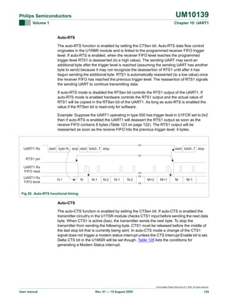
![UM10139
Philips Semiconductors
Volume 1
Chapter 10: UART1
Table 126: Modem status interrupt generation
Enable Modem CTSen
Status
(U1MCR[7])
Interrupt
(U1IER[3])
CTS Interrupt Delta CTS
Delta DCD or
Modem Status
Enable
(U1MSR[0]) Trailing Edge RI or
Interrupt
Delta DSR
(U1IER[7])
(U1MSR[3] or U1MSR[2] or (U1MSR[1]))
0
x
x
x
x
no
1
0
x
0
0
no
1
0
x
1
x
yes
1
0
x
x
1
yes
1
1
0
x
0
no
1
1
0
x
1
yes
1
1
1
0
0
no
1
1
1
1
x
yes
1
1
1
x
1
yes
start bits0..7 stop
start bits0..7 stop
start bits0..7 stop
~
~
UART1 Tx
~
~
~
~
The auto-CTS function reduces interrupts to the host system. When flow control is
enabled, a CTS1 state change does not trigger host interrupts because the device
automatically controls its own transmitter. Without auto-CTS, the transmitter sends any
data present in the transmit FIFO and a receiver overrun error can result. Figure 21
illustrates the auto-CTS functional timing.
~
~
CTS1 pin
Fig 21. Auto-CTS functional timing
While starting transmission of the initial character the CTS1 signal is asserted.
Transmission will stall as soon as the pending transmission has completed. The UART will
continue transmitting a 1 bit as long as CTS1 is deasserted (high). As soon as CTS1 gets
deasserted transmission resumes and a start bit is sent followed by the data bits of the
next character.
10.3.11 UART1 Line Status Register (U1LSR - 0xE001 0014, Read Only)
The U1LSR is a read-only register that provides status information on the UART1 TX and
RX blocks.
Table 127: UART1 Line Status Register (U1LSR - address 0xE001 0014, read only) bit description
Bit Symbol
0
Receiver Data
Ready
(RDR)
Value Description
Reset
value
U1LSR[0] is set when the U1RBR holds an unread character and is cleared when
the UART1 RBR FIFO is empty.
0
U1RBR is empty.
1
0
U1RBR contains valid data.
© Koninklijke Philips Electronics N.V. 2005. All rights reserved.
User manual
Rev. 01 — 15 August 2005
125](https://image.slidesharecdn.com/armusrmanl-131212220701-phpapp02/85/Arm-usr-m-anl-125-320.jpg)
![UM10139
Philips Semiconductors
Volume 1
Chapter 10: UART1
Table 127: UART1 Line Status Register (U1LSR - address 0xE001 0014, read only) bit description
Bit Symbol
1
Value Description
Overrun Error
(OE)
Reset
value
The overrun error condition is set as soon as it occurs. An U1LSR read clears
0
U1LSR[1]. U1LSR[1] is set when UART1 RSR has a new character assembled and
the UART1 RBR FIFO is full. In this case, the UART1 RBR FIFO will not be
overwritten and the character in the UART1 RSR will be lost.
0
1
2
Overrun error status is inactive.
Overrun error status is active.
Parity Error
(PE)
When the parity bit of a received character is in the wrong state, a parity error
occurs. An U1LSR read clears U1LSR[2]. Time of parity error detection is
dependent on U1FCR[0].
0
Note: A parity error is associated with the character at the top of the UART1 RBR
FIFO.
0
1
3
Parity error status is inactive.
Parity error status is active.
Framing Error
(FE)
When the stop bit of a received character is a logic 0, a framing error occurs. An
0
U1LSR read clears U1LSR[3]. The time of the framing error detection is dependent
on U1FCR0. Upon detection of a framing error, the RX will attempt to resynchronize
to the data and assume that the bad stop bit is actually an early start bit. However, it
cannot be assumed that the next received byte will be correct even if there is no
Framing Error.
Note: A framing error is associated with the character at the top of the UART1 RBR
FIFO.
0
1
4
Framing error status is inactive.
Framing error status is active.
Break Interrupt
(BI)
When RXD1 is held in the spacing state (all 0’s) for one full character transmission 0
(start, data, parity, stop), a break interrupt occurs. Once the break condition has
been detected, the receiver goes idle until RXD1 goes to marking state (all 1’s). An
U1LSR read clears this status bit. The time of break detection is dependent on
U1FCR[0].
Note: The break interrupt is associated with the character at the top of the UART1
RBR FIFO.
0
5
6
Transmitter
Holding
Register Empty
(THRE)
Transmitter
Empty
(TEMT)
Break interrupt status is inactive.
1
Break interrupt status is active.
THRE is set immediately upon detection of an empty UART1 THR and is cleared on 1
a U1THR write.
0
U1THR contains valid data.
1
U1THR is empty.
TEMT is set when both U1THR and U1TSR are empty; TEMT is cleared when
either the U1TSR or the U1THR contain valid data.
U1THR and/or the U1TSR contains valid data.
1
7
0
1
U1THR and the U1TSR are empty.
Error in RX
FIFO
(RXFE)
U1LSR[7] is set when a character with a RX error such as framing error, parity error 0
or break interrupt, is loaded into the U1RBR. This bit is cleared when the U1LSR
register is read and there are no subsequent errors in the UART1 FIFO.
0
U1RBR contains no UART1 RX errors or U1FCR[0]=0.
1
UART1 RBR contains at least one UART1 RX error.
© Koninklijke Philips Electronics N.V. 2005. All rights reserved.
User manual
Rev. 01 — 15 August 2005
126](https://image.slidesharecdn.com/armusrmanl-131212220701-phpapp02/85/Arm-usr-m-anl-126-320.jpg)
![UM10139
Philips Semiconductors
Volume 1
Chapter 10: UART1
10.3.12 UART1 Modem Status Register (U1MSR - 0xE001 0018), LPC2144/6/8
only
The U1MSR is a read-only register that provides status information on the modem input
signals. U1MSR[3:0] is cleared on U1MSR read. Note that modem signals have no direct
affect on UART1 operation, they facilitate software implementation of modem signal
operations.
Table 128: UART1 Modem Status Register (U1MSR - address 0xE001 0018), LPC2144/6/8 only bit description
Bit Symbol
0
Value Description
Delta CTS
Reset value
Set upon state change of input CTS. Cleared on an U1MSR read.
0
No change detected on modem input, CTS.
1
1
State change detected on modem input, CTS.
Delta DSR
Set upon state change of input DSR. Cleared on an U1MSR read.
0
State change detected on modem input, DSR.
Trailing Edge RI
Set upon low to high transition of input RI. Cleared on an U1MSR read.
0
0
No change detected on modem input, RI.
1
3
0
No change detected on modem input, DSR.
1
2
0
Low-to-high transition detected on RI.
Delta DCD
Set upon state change of input DCD. Cleared on an U1MSR read.
0
No change detected on modem input, DCD.
1
0
State change detected on modem input, DCD.
4
CTS
Clear To Send State. Complement of input signal CTS. This bit is connected
to U1MCR[1] in modem loopback mode.
0
5
DSR
Data Set Ready State. Complement of input signal DSR. This bit is connected 0
to U1MCR[0] in modem loopback mode.
6
RI
Ring Indicator State. Complement of input RI. This bit is connected to
U1MCR[2] in modem loopback mode.
7
DCD
Data Carrier Detect State. Complement of input DCD. This bit is connected to 0
U1MCR[3] in modem loopback mode.
0
10.3.13 UART1 Scratch pad register (U1SCR - 0xE001 001C)
The U1SCR has no effect on the UART1 operation. This register can be written and/or
read at user’s discretion. There is no provision in the interrupt interface that would indicate
to the host that a read or write of the U1SCR has occurred.
Table 129: UART1 Scratch pad register (U1SCR - address 0xE001 0014) bit description
Bit
Symbol
Description
Reset value
7:0
Pad
A readable, writable byte.
0x00
10.3.14 UART1 Auto-baud Control Register (U1ACR - 0xE001 0020)
The UART1 Auto-baud Control Register (U1ACR) controls the process of measuring the
incoming clock/data rate for the baud rate generation and can be read and written at
user’s discretion.
© Koninklijke Philips Electronics N.V. 2005. All rights reserved.
User manual
Rev. 01 — 15 August 2005
127](https://image.slidesharecdn.com/armusrmanl-131212220701-phpapp02/85/Arm-usr-m-anl-127-320.jpg)
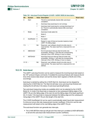
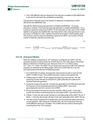
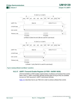
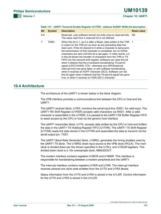
![UM10139
Philips Semiconductors
Volume 1
Chapter 10: UART1
MODEM
U1TX
U1THR
CTS
DSR
NTXRDY
U1TSR
TXD1
U1MSR
RI
U1BRG
DCD
DTR
U1DLL
NBAUDOUT
U1DLM
RTS
RCLK
U1MCR
U1RX
NRXRDY
INTERRUPT
U1RBR
U1INTR
U1RSR
RXD1
U1IER
U1IIR
U1FCR
U1LSR
U1SCR
U1LCR
PA[2:0]
PSEL
PSTB
PWRITE
VPB
INTERFACE
PD[7:0]
DDIS
AR
MR
PCLK
Fig 23. UART1 block diagram
© Koninklijke Philips Electronics N.V. 2005. All rights reserved.
User manual
Rev. 01 — 15 August 2005
132](https://image.slidesharecdn.com/armusrmanl-131212220701-phpapp02/85/Arm-usr-m-anl-132-320.jpg)
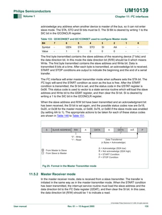
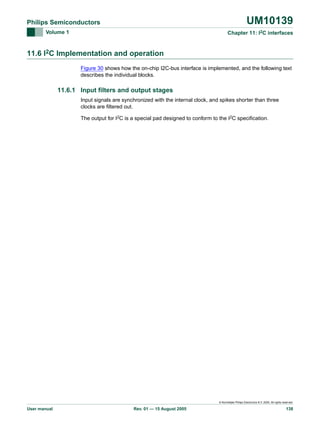
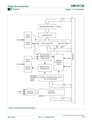
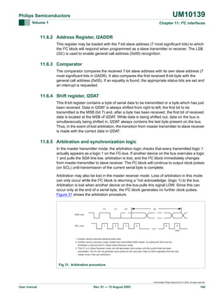
![UM10139
Philips Semiconductors
Volume 1
Chapter 11: I2C interfaces
The contents of the I2C control register may be read as I2CONSET. Writing to I2CONSET
will set bits in the I2C control register that correspond to ones in the value written.
Conversely, writing to I2CONCLR will clear bits in the I2C control register that correspond
to ones in the value written.
11.6.9 Status decoder and Status register
The status decoder takes all of the internal status bits and compresses them into a 5-bit
code. This code is unique for each I2C-bus status. The 5-bit code may be used to
generate vector addresses for fast processing of the various service routines. Each
service routine processes a particular bus status. There are 26 possible bus states if all
four modes of the I2C block are used. The 5-bit status code is latched into the five most
significant bits of the status register when the serial interrupt flag is set (by hardware) and
remains stable until the interrupt flag is cleared by software. The three least significant bits
of the status register are always zero. If the status code is used as a vector to service
routines, then the routines are displaced by eight address locations. Eight bytes of code is
sufficient for most of the service routines (see the software example in this section).
11.7 Register description
Each I2C interface contains 7 registers as shown in Table 135 below.
Table 135: I2C register map
Name
Access Reset
I2C0 Address I2C1 Address
[1] and Name
value
and Name
Description
I2CONSET I2C Control Set Register. When a one is written to a bit
of this register, the corresponding bit in the I2C control
register is set. Writing a zero has no effect on the
corresponding bit in the I2C control register.
R/W
0x00
0xE001 C000 0xE005 C000
I2C0CONSET I2C1CONSET
RO
0xF8
0xE001 C004
I2C0STAT
0xE005 C004
I2C1STAT
I2STAT
I2C Status Register. During I2C operation, this register
provides detailed status codes that allow software to
determine the next action needed.
I2DAT
I2C Data Register. During master or slave transmit mode, R/W
data to be transmitted is written to this register. During
master or slave receive mode, data that has been
received may be read from this register.
0x00
0xE001 C008
I2C0DAT
0xE005 C008
I2C1DAT
I2ADR
I2C Slave Address Register. Contains the 7-bit slave
address for operation of the I2C interface in slave mode,
and is not used in master mode. The least significant bit
determines whether a slave responds to the general call
address.
R/W
0x00
0xE001 C00C
I2C0ADR
0xE005 C00C
I2C1ADR
I2SCLH
SCH Duty Cycle Register High Half Word. Determines
the high time of the I2C clock.
R/W
0x04
0xE001 C010
I2C0SCLH
0xE005 C010
I2C1SCLH
I2SCLL
SCL Duty Cycle Register Low Half Word. Determines
the low time of the I2C clock. I2nSCLL and I2nSCLH
together determine the clock frequency generated by an
I2C master and certain times used in slave mode.
R/W
0x04
0xE001 C014
I2C0SCLL
0xE005 C014
I2C1SCLL
NA
0xE001 C018 0xE005 C018
I2C0CONCLR I2C1CONCLR
I2CONCLR I2C Control Clear Register. When a one is written to a
WO
bit of this register, the corresponding bit in the I2C control
register is cleared. Writing a zero has no effect on the
corresponding bit in the I2C control register.
[1]
Reset value reflects the data stored in used bits only. It does not include reserved bits content.
© Koninklijke Philips Electronics N.V. 2005. All rights reserved.
User manual
Rev. 01 — 15 August 2005
142](https://image.slidesharecdn.com/armusrmanl-131212220701-phpapp02/85/Arm-usr-m-anl-142-320.jpg)
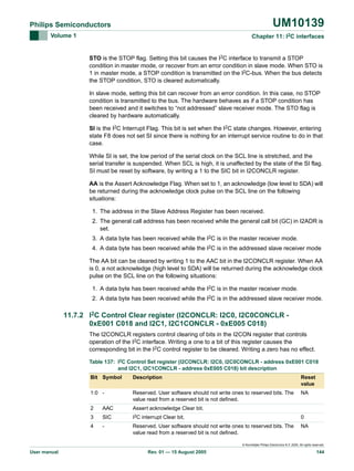
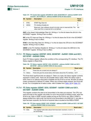
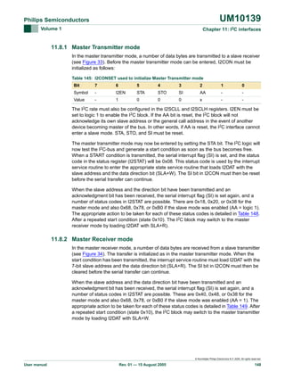
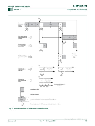
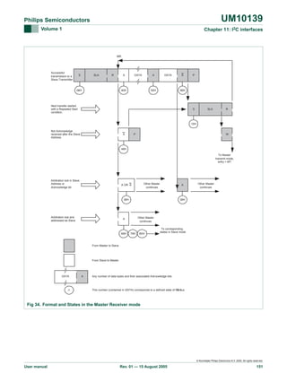
![UM10139
Philips Semiconductors
Volume 1
Chapter 11: I2C interfaces
Table 150: Slave Receiver mode
Status
Status of the I2C-bus Application software response
Code
and hardware
To/From I2DAT
To I2CON
(I2CSTAT)
STA STO SI
Next action taken by I2C hardware
AA
0x60
0x78
0x80
0x88
0x90
0
0
0
Data byte will be received and NOT ACK
will be returned.
No I2DAT action
X
0
0
1
Data byte will be received and ACK will
be returned.
Arbitration lost in
SLA+R/W as master;
Own SLA+W has
been received, ACK
returned.
No I2DAT action or X
0
0
0
Data byte will be received and NOT ACK
will be returned.
No I2DAT action
X
0
0
1
Data byte will be received and ACK will
be returned.
General call address
(0x00) has been
received; ACK has
been returned.
No I2DAT action or X
0
0
0
Data byte will be received and NOT ACK
will be returned.
No I2DAT action
X
0
0
1
Data byte will be received and ACK will
be returned.
Arbitration lost in
SLA+R/W as master;
General call address
has been received,
ACK has been
returned.
No I2DAT action or X
0
0
0
Data byte will be received and NOT ACK
will be returned.
No I2DAT action
X
0
0
1
Data byte will be received and ACK will
be returned.
Previously addressed
with own SLV
address; DATA has
been received; ACK
has been returned.
Read data byte or X
0
0
0
Data byte will be received and NOT ACK
will be returned.
Read data byte
X
0
0
1
Data byte will be received and ACK will
be returned.
Previously addressed
with own SLA; DATA
byte has been
received; NOT ACK
has been returned.
Read data byte or 0
0
0
0
Switched to not addressed SLV mode; no
recognition of own SLA or General call
address.
Read data byte or 0
0
0
1
Switched to not addressed SLV mode;
Own SLA will be recognized; General call
address will be recognized if
I2ADR[0] = logic 1.
0
0
0
Switched to not addressed SLV mode; no
recognition of own SLA or General call
address. A START condition will be
transmitted when the bus becomes free.
Read data byte
0x70
No I2DAT action or X
Read data byte or 1
0x68
Own SLA+W has
been received; ACK
has been returned.
1
0
0
1
Switched to not addressed SLV mode;
Own SLA will be recognized; General call
address will be recognized if
I2ADR[0] = logic 1. A START condition
will be transmitted when the bus becomes
free.
Read data byte or X
0
0
0
Data byte will be received and NOT ACK
will be returned.
Read data byte
0
0
1
Data byte will be received and ACK will
be returned.
Previously addressed
with General Call;
DATA byte has been
received; ACK has
been returned.
X
© Koninklijke Philips Electronics N.V. 2005. All rights reserved.
User manual
Rev. 01 — 15 August 2005
156](https://image.slidesharecdn.com/armusrmanl-131212220701-phpapp02/85/Arm-usr-m-anl-156-320.jpg)
![UM10139
Philips Semiconductors
Volume 1
Chapter 11: I2C interfaces
Table 150: Slave Receiver mode
Status
Status of the I2C-bus Application software response
Code
and hardware
To/From I2DAT
To I2CON
(I2CSTAT)
STA STO SI
AA
0x98
0
0
0
Switched to not addressed SLV mode; no
recognition of own SLA or General call
address.
Read data byte or 0
0
0
1
Switched to not addressed SLV mode;
Own SLA will be recognized; General call
address will be recognized if
I2ADR[0] = logic 1.
0
0
0
Switched to not addressed SLV mode; no
recognition of own SLA or General call
address. A START condition will be
transmitted when the bus becomes free.
Read data byte
1
0
0
1
Switched to not addressed SLV mode;
Own SLA will be recognized; General call
address will be recognized if
I2ADR[0] = logic 1. A START condition
will be transmitted when the bus becomes
free.
No STDAT action
or
0
0
0
0
Switched to not addressed SLV mode; no
recognition of own SLA or General call
address.
No STDAT action
or
0
0
0
1
Switched to not addressed SLV mode;
Own SLA will be recognized; General call
address will be recognized if
I2ADR[0] = logic 1.
No STDAT action
or
1
0
0
0
Switched to not addressed SLV mode; no
recognition of own SLA or General call
address. A START condition will be
transmitted when the bus becomes free.
No STDAT action
A STOP condition or
repeated START
condition has been
received while still
addressed as
SLV/REC or SLV/TRX.
Read data byte or 0
Read data byte or 1
0xA0
Previously addressed
with General Call;
DATA byte has been
received; NOT ACK
has been returned.
Next action taken by I2C hardware
1
0
0
1
Switched to not addressed SLV mode;
Own SLA will be recognized; General call
address will be recognized if
I2ADR[0] = logic 1. A START condition
will be transmitted when the bus becomes
free.
© Koninklijke Philips Electronics N.V. 2005. All rights reserved.
User manual
Rev. 01 — 15 August 2005
157](https://image.slidesharecdn.com/armusrmanl-131212220701-phpapp02/85/Arm-usr-m-anl-157-320.jpg)
![UM10139
Philips Semiconductors
Volume 1
Chapter 11: I2C interfaces
Table 151: Slave Transmitter mode
Status
Status of the I2C-bus Application software response
Code
and hardware
To/From I2DAT
To I2CON
(I2CSTAT)
STA STO SI
Next action taken by I2C hardware
AA
0xA8
0
Last data byte will be transmitted and
ACK bit will be received.
X
0
0
1
Data byte will be transmitted; ACK will be
received.
Arbitration lost in
Load data byte or
SLA+R/W as master;
Own SLA+R has been Load data byte
received, ACK has
been returned.
X
0
0
0
Last data byte will be transmitted and
ACK bit will be received.
X
0
0
1
Data byte will be transmitted; ACK bit will
be received.
Data byte in I2DAT
Load data byte or
has been transmitted;
ACK has been
Load data byte
received.
X
0
0
0
Last data byte will be transmitted and
ACK bit will be received.
X
0
0
1
Data byte will be transmitted; ACK bit will
be received.
Data byte in I2DAT
No I2DAT action or 0
has been transmitted;
NOT ACK has been
received.
No I2DAT action or 0
0
0
0
Switched to not addressed SLV mode; no
recognition of own SLA or General call
address.
0
0
1
Switched to not addressed SLV mode;
Own SLA will be recognized; General call
address will be recognized if
I2ADR[0] = logic 1.
0
0
0
Switched to not addressed SLV mode; no
recognition of own SLA or General call
address. A START condition will be
transmitted when the bus becomes free.
1
0
0
1
Switched to not addressed SLV mode;
Own SLA will be recognized; General call
address will be recognized if
I2ADR[0] = logic 1. A START condition
will be transmitted when the bus becomes
free.
No I2DAT action or 0
0
0
0
Switched to not addressed SLV mode; no
recognition of own SLA or General call
address.
No I2DAT action or 0
0
0
1
Switched to not addressed SLV mode;
Own SLA will be recognized; General call
address will be recognized if
I2ADR[0] = logic 1.
0
0
0
Switched to not addressed SLV mode; no
recognition of own SLA or General call
address. A START condition will be
transmitted when the bus becomes free.
No I2DAT action
0xC8
0
No I2DAT action or 1
0xC0
0
No I2DAT action
0xB8
X
No I2DAT action or 1
0xB0
Own SLA+R has been Load data byte or
received; ACK has
been returned.
Load data byte
0
0
01
Switched to not addressed SLV mode;
Own SLA will be recognized; General call
address will be recognized if
I2ADR.0 = logic 1. A START condition will
be transmitted when the bus becomes
free.
Last data byte in
I2DAT has been
transmitted (AA = 0);
ACK has been
received.
1
© Koninklijke Philips Electronics N.V. 2005. All rights reserved.
User manual
Rev. 01 — 15 August 2005
158](https://image.slidesharecdn.com/armusrmanl-131212220701-phpapp02/85/Arm-usr-m-anl-158-320.jpg)
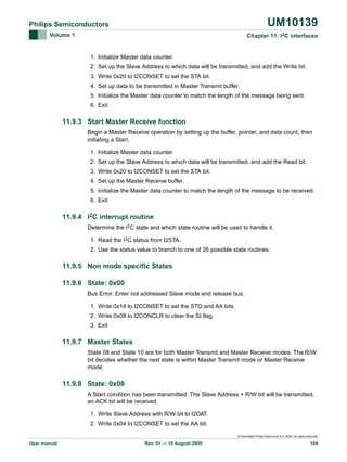
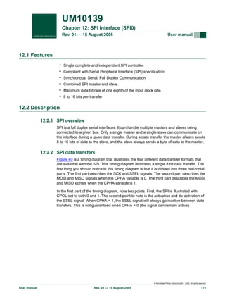
![UM10139
Philips Semiconductors
Volume 1
Chapter 12: SPI
Table 155: SPI register map
Name
Description
Access
Reset
value[1]
Address
S0SPCR
SPI Control Register. This register controls the
operation of the SPI.
R/W
0x00
0xE002 0000
S0SPSR
SPI Status Register. This register shows the
status of the SPI.
RO
0x00
0xE002 0004
S0SPDR
SPI Data Register. This bi-directional register
R/W
provides the transmit and receive data for the
SPI. Transmit data is provided to the SPI0 by
writing to this register. Data received by the SPI0
can be read from this register.
0x00
0xE002 0008
S0SPCCR SPI Clock Counter Register. This register
controls the frequency of a master’s SCK0.
R/W
0x00
0xE002 000C
S0SPINT
R/W
0x00
0xE002 001C
[1]
SPI Interrupt Flag. This register contains the
interrupt flag for the SPI interface.
Reset value reflects the data stored in used bits only. It does not include reserved bits content.
12.4.1 SPI Control Register (S0SPCR - 0xE002 0000)
The S0SPCR register controls the operation of the SPI0 as per the configuration bits
setting.
Table 156: SPI Control Register (S0SPCR - address 0xE002 0000) bit description
Bit
Symbol
1:0
-
2
BitEnable
Value Description
Reset
value
NA
0
The SPI controller sends and receives 8 bits of data per
transfer.
0
1
3
Reserved, user software should not write ones to
reserved bits. The value read from a reserved bit is not
defined.
The SPI controller sends and receives the number of bits
selected by bits 11:8.
CPHA
Clock phase control determines the relationship between 0
the data and the clock on SPI transfers, and controls
when a slave transfer is defined as starting and ending.
0
1
4
CPOL
Data is sampled on the first clock edge of SCK. A transfer
starts and ends with activation and deactivation of the
SSEL signal.
Data is sampled on the second clock edge of the SCK. A
transfer starts with the first clock edge, and ends with the
last sampling edge when the SSEL signal is active.
Clock polarity control.
0
1
5
0
SCK is active high.
SCK is active low.
MSTR
Master mode select.
0
1
0
The SPI operates in Slave mode.
The SPI operates in Master mode.
© Koninklijke Philips Electronics N.V. 2005. All rights reserved.
User manual
Rev. 01 — 15 August 2005
176](https://image.slidesharecdn.com/armusrmanl-131212220701-phpapp02/85/Arm-usr-m-anl-176-320.jpg)
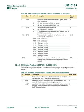
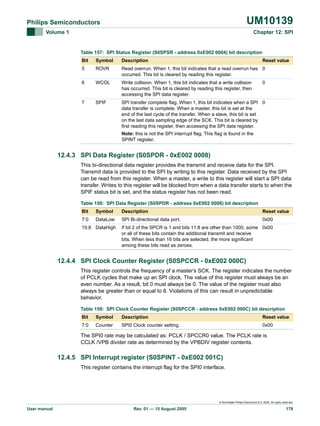
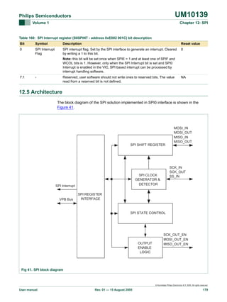
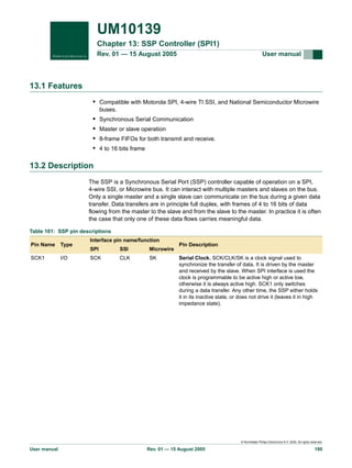
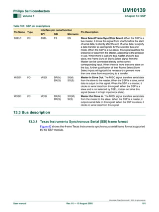
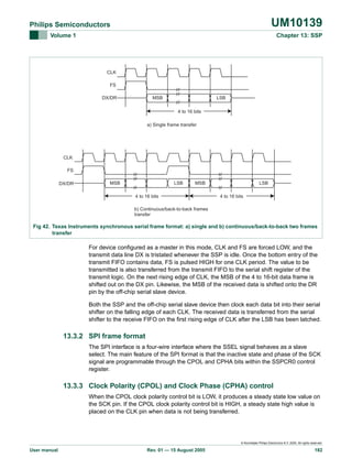
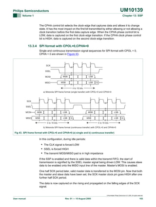
![UM10139
Philips Semiconductors
Volume 1
Chapter 13: SSP
Table 162: SSP register map
Description
SSPCR0
Control Register 0. Selects the serial clock R/W
rate, bus type, and data size.
0x0000
0xE006 8000
SSPCR1
Control Register 1. Selects master/slave
and other modes.
0x00
0xE006 8004
SSPDR
Data Register. Writes fill the transmit FIFO, R/W
and reads empty the receive FIFO.
0x0000
0xE006 8008
SSPSR
Status Register
RO
0x03
0xE006 800C
SSPCPSR Clock Prescale Register
R/W
0x00
0xE006 8010
SSPIMSC
Interrupt Mask Set and Clear Register
R/W
0x00
0xE006 8014
SSPRIS
Raw Interrupt Status Register
R/W
0x04
0xE006 8018
SSPMIS
Masked Interrupt Status Register
RO
0x00
0xE006 801C
SSPICR
SSPICR Interrupt Clear Register
WO
NA
0xE006 8020
[1]
Access
Reset value[1] Address
Name
R/W
Reset value reflects the data stored in used bits only. It does not include reserved bits content.
13.4.1 SSP Control Register 0 (SSPCR0 - 0xE006 8000)
This register controls the basic operation of the SSP controller.
Table 163: SSP Control Register 0 (SSPCR0 - address 0xE006 8000) bit description
Bit
Symbol
3:0
Value
DSS
Description
Reset
value
Data Size Select. This field controls the number of bits
transferred in each frame. Values 0000-0010 are not
supported and should not be used.
0000
0011
5 bit transfer
0101
6 bit transfer
0110
7 bit transfer
0111
8 bit transfer
1000
9 bit transfer
1001
10 bit transfer
1010
11 bit transfer
1011
12 bit transfer
1100
13 bit transfer
1101
14 bit transfer
1110
15 bit transfer
1111
5:4
4 bit transfer
0100
16 bit transfer
FRF
Frame Format.
00
00
SPI
01
SSI
10
Microwire
11
This combination is not supported and should not be used.
© Koninklijke Philips Electronics N.V. 2005. All rights reserved.
User manual
Rev. 01 — 15 August 2005
189](https://image.slidesharecdn.com/armusrmanl-131212220701-phpapp02/85/Arm-usr-m-anl-189-320.jpg)
![UM10139
Philips Semiconductors
Volume 1
Chapter 13: SSP
Table 163: SSP Control Register 0 (SSPCR0 - address 0xE006 8000) bit description
Bit
Symbol
6
Value
Description
CPOL
Clock Out Polarity. This bit is only used in SPI mode.
0
SSP controller captures serial data on the first clock transition
of the frame, that is, the transition away from the inter-frame
state of the clock line.
0
1
7
Reset
value
SSP controller captures serial data on the second clock
transition of the frame, that is, the transition back to the
inter-frame state of the clock line.
CPHA
Clock Out Phase. This bit is only used in SPI mode.
0
1
15:8
0
SSP controller maintains the bus clock low between frames.
SSP controller maintains the bus clock high between frames.
SCR
Serial Clock Rate. The number of prescaler-output clocks per 0x00
bit on the bus, minus one. Given that CPSDVR is the prescale
divider, and the VPB clock PCLK clocks the prescaler, the bit
frequency is PCLK / (CPSDVSR * [SCR+1]).
13.4.2 SSP Control Register 1 (SSPCR1 - 0xE006 8004)
This register controls certain aspects of the operation of the SSP controller.
Table 164: SSP Control Register 1 (SSPCR1 - address 0xE006 8004) bit description
Bit
Symbol
0
Value
LBM
Description
Reset
value
Loop Back Mode.
0
0
1
1
During normal operation.
Serial input is taken from the serial output (MOSI or MISO)
rather than the serial input pin (MISO or MOSI
respectively).
SSE
SSP Enable.
0
0
2
The SSP controller is disabled.
1
The SSP controller will interact with other devices on the
serial bus. Software should write the appropriate control
information to the other SSP registers and interrupt
controller registers, before setting this bit.
MS
Master/Slave Mode.This bit can only be written when the
SSE bit is 0.
0
1
0
The SSP controller acts as a master on the bus, driving the
SCLK, MOSI, and SSEL lines and receiving the MISO line.
The SSP controller acts as a slave on the bus, driving
MISO line and receiving SCLK, MOSI, and SSEL lines.
3
SOD
Slave Output Disable. This bit is relevant only in slave
mode (MS = 1). If it is 1, this blocks this SSP controller
from driving the transmit data line (MISO).
0
7:4
-
Reserved, user software should not write ones to reserved NA
bits. The value read from a reserved bit is not defined.
© Koninklijke Philips Electronics N.V. 2005. All rights reserved.
User manual
Rev. 01 — 15 August 2005
190](https://image.slidesharecdn.com/armusrmanl-131212220701-phpapp02/85/Arm-usr-m-anl-190-320.jpg)
![UM10139
Philips Semiconductors
Volume 1
Chapter 14: USB Device Controller
Table 174: USB device register map
Name
Access
Description
Reset value[1]
Address
Device interrupt registers
USBIntSt
USB Interrupt Status
R/W
0x8000 0000
0xE01F C1C0
USBDevIntSt
USB Device Interrupt Status
RO
0x0000 0010
0xE009 0000
USBDevIntEn
USB Device Interrupt Enable
R/W
0x0000 0000
0xE009 0004
USBDevIntClr
USB Device Interrupt Clear
WO
0x0000 0000
0xE009 0008
USBDevIntSet
USB Device Interrupt Set
WO
0x0000 0000
0xE009 000C
USBDevIntPri
USB Device Interrupt Priority
WO
0x00
0xE009 002C
Endpoint interrupt registers
USBEpIntSt
USB Endpoint Interrupt Status
RO
0x0000 0000
0xE009 0030
USBEpIntEn
USB Endpoint Interrupt Enable
R/W
0x0000 0000
0xE009 0034
USBEpIntClr
USB Endpoint Interrupt Clear
WO
0x0000 0000
0xE009 0038
USBEpIntSet
USB Endpoint Interrupt Set
WO
0x0000 0000
0xE009 003C
USBEpIntPri
USB Endpoint Priority
WO
0x0000 0000
0xE009 0040
Endpoint realization registers
USBReEp
USB Realize Endpoint
R/W
0x0000 0003
0xE009 0044
USBEpInd
USB Endpoint Index
WO
0x0000 0000
0xE009 0048
USBMaxPSize
USB MaxPacketSize
R/W
0x0000 0008
0xE009 004C
USBRxData
USB Receive Data
RO
0x0000 0000
0xE009 0018
USBRxPLen
USB Receive Packet Length
RO
0x0000 0000
0xE009 0020
USBTxData
USB Transmit Data
WO
0x0000 0000
0xE009 001C
USBTxPLen
USB Transmit Packet Length
WO
0x0000 0000
0xE009 0024
USBCtrl
USB Control
R/W
0x0000 0000
0xE009 0028
USBCmdCode
USB Command Code
WO
0x0000 0000
0xE009 0010
USBCmdData
USB Command Data
RO
0x0000 0000
0xE009 0014
USB transfer registers
Command registers
DMA registers (LPC2146/8 only)
USBDMARSt
USB DMA Request Status
RO
0x0000 0000
0xE009 0050
USBDMARClr
USB DMA Request Clear
WO
0x0000 0000
0xE009 0054
USBDMARSet
USB DMA Request Set
WO
0x0000 0000
0xE009 0058
USBUDCAH
USB UDCA Head
R/W
0x0000 0000
0xE009 0080
USBEpDMASt
USB Endpoint DMA Status
RO
0x0000 0000
0xE009 0084
USBEpDMAEn
USB Endpoint DMA Enable
WO
0x0000 0000
0xE009 0088
USBEpDMADis
USB Endpoint DMA Disable
WO
0x0000 0000
0xE009 008C
USBDMAIntSt
USB DMA Interrupt Status
RO
0x0000 0000
0xE009 0090
USBDMAIntEn
USB DMA Interrupt Enable
R/W
0x0000 0000
0xE009 0094
USBEoTIntSt
USB End of Transfer Interrupt Status
RO
0x0000 0000
0xE009 00A0
USBEoTIntClr
USB End of Transfer Interrupt Clear
WO
0x0000 0000
0xE009 00A4
USBEoTIntSet
USB End of Transfer Interrupt Set
WO
0x0000 0000
0xE009 00A8
USBNDDRIntSt
USB New DD Request Interrupt Status
RO
0x0000 0000
0xE009 00AC
USBNDDRIntClr
USB New DD Request Interrupt Clear
WO
0x0000 0000
0xE009 00B0
9397 750 XXXXX
User manual
© Koninklijke Philips Electronics N.V. 2005. All rights reserved.
Rev. 01 — 15 August 2005
199](https://image.slidesharecdn.com/armusrmanl-131212220701-phpapp02/85/Arm-usr-m-anl-199-320.jpg)
![UM10139
Philips Semiconductors
Volume 1
Chapter 14: USB Device Controller
Table 174: USB device register map
Name
Description
Access
Reset value[1]
Address
USBNDDRIntSet
USB New DD Request Interrupt Set
WO
0x0000 0000
0xE009 00B4
USBSysErrIntSt
USB System Error Interrupt Status
RO
0x0000 0000
0xE009 00B8
USBSysErrIntClr
USB System Error Interrupt Clear
WO
0x0000 0000
0xE009 00BC
USBSysErrIntSet
USB System Error Interrupt Set
WO
0x0000 0000
0xE009 00C0
[1]
Reset value reflects the data stored in used bits only. It does not include reserved bits content.
14.7 USB Device register definitions
14.7.1 USB Interrupt Status register (USBIntSt - 0xE01F C1C0)
The USB device has three interrupt output lines. The interrupts usb_int_req_Ip and
usb_int_req_hp facilitates transfer of data in slave mode. These two interrupt lines are
provided to allow two different priority (high/low) levels in slave mode transfer. Each of the
individual endpoint interrupts can be routed to either high priority or low priority levels
using corresponding bits in the Endpoint Interrupt Priority register (Section 14.7.11). The
interrupt level is triggered with active high polarity. The external interrupt generation takes
place only if the necessary ‘enable’ bits are set in the Device Interrupt Enable register
(Section 14.7.3). Otherwise, they will be registered only in the status registers. The
usb_int_req_dma is raised when an end_of_transfer or a system error has occurred. DMA
data transfer is not dependent on this interrupt.
The three interrupt output lines are ORed together to reduce the number of interrupt
channels required for the USB device in the vectored interrupt controller. This register
reflects the status of the each interrupt line. The USBIntSt is a read/write register.
Table 175: USB Interrupt Status register (USBIntSt - address 0xE01F C1C0) bit description
Bit
Symbol
Description
Reset
value
0
USB_INT_REQ_LP
Low priority interrupt line status. This bit is read only.
0
1
USB_INT_REQ_HP
High priority interrupt line status. This bit is read only.
0
2
USB_INT_REQ_DMA
DMA interrupt line status. This bit is read only. (LPC2146/8 only)
0
7:3
-
Reserved, user software should not write ones to reserved bits. The
value read from a reserved bit is not defined.
NA
9397 750 XXXXX
User manual
© Koninklijke Philips Electronics N.V. 2005. All rights reserved.
Rev. 01 — 15 August 2005
200](https://image.slidesharecdn.com/armusrmanl-131212220701-phpapp02/85/Arm-usr-m-anl-200-320.jpg)
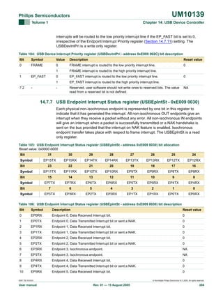
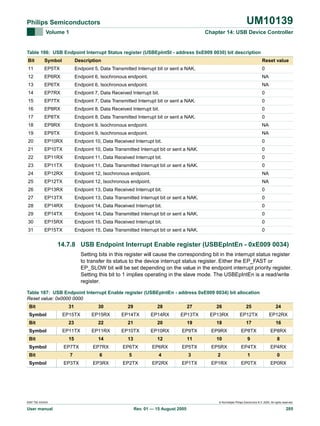
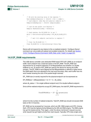
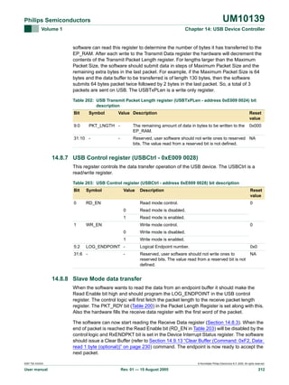
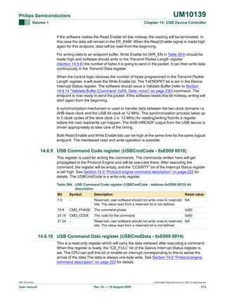
![UM10139
Philips Semiconductors
Volume 1
Chapter 14: USB Device Controller
Table 205: USB Command Data register (USBCmdData - address 0xE009 0014) bit
description
Bit
Symbol
7:0
CommandData Command Data.
Description
31:8
-
Reset value
0x00
Reserved, user software should not write ones to reserved NA
bits. The value read from a reserved bit is not defined.
14.8.11 USB DMA Request Status register (USBDMARSt - 0xE009 0050)
This register is set by the hardware whenever a packet (OUT) or token (IN) is received on
a realized endpoint. It serves as a flag for DMA engine to start the data transfer if the DMA
is enabled for this particular endpoint. Each endpoint has one reserved bit in this register.
Hardware sets this bit when a realized endpoint needs to be serviced through DMA.
Software can read the register content. DMA cannot be enabled for control endpoints
(EP0 and EP1). For easy readability the control endpoint is shown in the register contents.
The USBDMARSt is a read only register.
Table 206: USB DMA Request Status register (USBDMARSt - address 0xE009 0050) bit allocation
Reset value: 0x0000 0000
Bit
31
EP30
EP29
EP28
EP27
EP26
EP25
EP24
22
21
20
19
18
17
16
EP22
EP21
EP20
EP19
EP18
EP17
EP16
14
13
12
11
10
9
8
EP14
EP13
EP12
EP11
EP10
EP9
EP8
6
5
4
3
2
1
0
EP7
Symbol
24
7
Bit
25
EP15
Symbol
26
15
Bit
27
EP23
Symbol
28
23
Bit
29
EP31
Symbol
30
EP6
EP5
EP4
EP3
EP2
EP1
EP0
Table 207: USB DMA Request Status register (USBDMARSt - address 0xE009 0050) bit description
Bit
Symbol
Value
Description
Reset value
0
EP0
0
Control endpoint OUT (DMA cannot be enabled for this endpoint and EP0
bit must be 0).
0
1
EP1
0
Control endpoint IN (DMA cannot be enabled for this endpoint and EP1 bit
must be 0).
0
31:2
EPxx
Endpoint xx (2 ≤ xx ≤ 31) DMA request.
0
0
DMA not requested by endpoint xx.
1
DMA requested by endpoint xx.
[1]
DMA can not be enabled for this endpoint and the corresponding bit in the USBDMARSt must be 0.
14.8.12 USB DMA Request Clear register (USBDMARClr - 0xE009 0054)
Writing 1 into the register will clear the corresponding interrupt from the DMA Request
Status register. Writing 0 will not have any effect. Also, after a packet transfer, the
hardware clears the particular bit in DMA Request Status register. The USBDMARClr is a
write only register.
The USBDMARClr bit allocation is identical to the USBDMARSt register (Table 206).
9397 750 XXXXX
User manual
© Koninklijke Philips Electronics N.V. 2005. All rights reserved.
Rev. 01 — 15 August 2005
214](https://image.slidesharecdn.com/armusrmanl-131212220701-phpapp02/85/Arm-usr-m-anl-214-320.jpg)
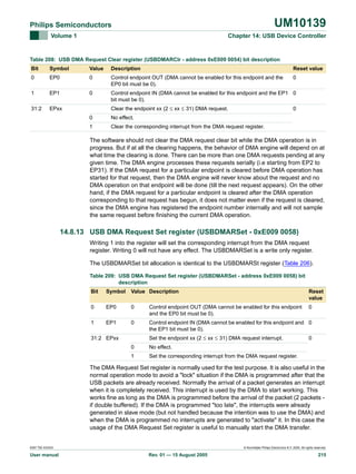
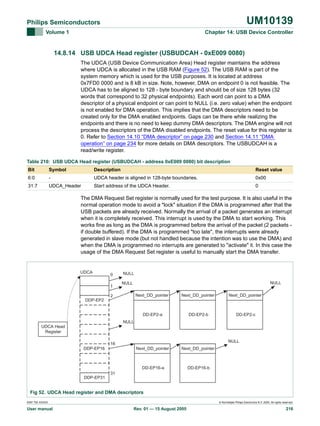
![UM10139
Philips Semiconductors
Volume 1
Chapter 14: USB Device Controller
Table 227: Configure Device Register bit description
Bit
Symbol
Description
Reset value
0
CONF_DEVICE
Device is configured. This bit is set after the set configuration command is 0
executed. Good link LED signal is asserted when configuration is done.
7:1
-
Reserved, user software should not write ones to reserved bits. The value NA
read from a reserved bit is not defined.
14.9.3 Set Mode (Command: 0xF3, Data: write 1 byte)
Table 228: Set Mode Register bit description
Bit
Symbol
0
Value Description
AP_CLK
Reset
value
Always PLL Clock.
0
0
1
1
usb_needclk is functional; 48 Mhz clock can be stopped when
the device enters suspend state.
usb_needclk always have the value 1. 48 Mhz clock cannot be
stopped in case when the device enters suspend state.
INAK_CI
Interrupt on NAK for Control IN endpoint.
0
Only successful transactions generate an interrupt.
1
2
Both successful and NAKed IN transactions generate interrupts.
INAK_CO
Interrupt on NAK for Control OUT endpoint.
0
Both successful and NAKed OUT transactions generate
interrupts.
INAK_II
Interrupt on NAK for Interrupt IN endpoint.
0
Both successful and NAKed IN transactions generate interrupts.
INAK_IO[1]
Interrupt on NAK for Interrupt OUT endpoints.
0
Both successful and NAKed OUT transactions generate
interrupts.
INAK_BI
Interrupt on NAK for Bulk IN endpoints.
0
0
Only successful transactions generate an interrupt.
1
6
0
Only successful transactions generate an interrupt.
1
5
0
Only successful transactions generate an interrupt.
1
4
0
Only successful transactions generate an interrupt.
1
3
0
Both successful and NAKed IN transactions generate interrupts.
INAK_BO[2]
Interrupt on NAK for Bulk OUT endpoints.
0
0
7
-
Only successful transactions generate an interrupt.
1
Both successful and NAKed OUT transactions generate
interrupts.
-
Reserved, user software should not write ones to reserved bits. NA
The value read from a reserved bit is not defined.
[1]
This bit should be reset to 0 if the DMA is enabled for any of the Interrupt OUT endpoints.
[2]
This bit should be reset to 0 if the DMA is enabled for any of the Bulk OUT endpoints.
9397 750 XXXXX
User manual
© Koninklijke Philips Electronics N.V. 2005. All rights reserved.
Rev. 01 — 15 August 2005
224](https://image.slidesharecdn.com/armusrmanl-131212220701-phpapp02/85/Arm-usr-m-anl-224-320.jpg)
![UM10139
Philips Semiconductors
Volume 1
Chapter 14: USB Device Controller
There are certain parameters associated with a DMA transfer. These are:
•
•
•
•
•
•
The start address of the DMA buffer in the USB RAM.
The length of the DMA Buffer in the USB RAM.
The start address of the next DMA buffer.
Control information.
DMA count information (Number of bytes transferred).
DMA status information.
Table 235 lists the DMA descriptor fields.
Table 235: DMA descriptor
Word
Access Access Bit
Description
position (H/W)
(S/W)
position
0
R
R/W
31:0
Next_DD_pointer (USB RAM address).
1
R
R/W
1:0
DMA_mode (00 -Normal; 01 - ATLE).
R
R/W
2
Next_DD_valid (1 - valid; 0 - invalid).
-
-
3
Reserved.
R
R/W
4
Isochronous_endpoint (1 - isochronous;
0 - non-isochronous).
R
R/W
15:5
Max_packet_size.
R/W[1]
R/W
31:16
DMA_buffer_length in bytes.
2
R/W
R/W
31:0
DMA_buffer_start_addr.
3
R/W
R/I
0
DD_retired (To be initialized to 0).
W
R/I
4:1
DD_status (To be initialized to 0):
0000 - Not serviced.
0001 - Being serviced.
0010 - Normal completion.
0011 - Data under run (short packet).
1000 - Data over run.
1001 - System error.
W
5
Packet_valid (To be initialized to 0).
W
R/I
6
LS_byte_extracted (ATLE mode) (To be initialized to 0).
W
R/I
7
MS_byte_extracted (ATLE mode) (To be initialized to 0).
R
W
13:8
Message_length_position (ATLE mode).
-
-
15:14
Reserved.
R/W
4
R/I
R/I
31:16
Present_DMA_count (To be initialized to 0).
R/W
R/W
31:0
Isochronous_packetsize_memory_address.
Legend: R - Read; W - Write; I - Initialize
[1]
Write only in ATLE mode
14.10.1 Next_DD_pointer
Pointer to the memory location from where the next DMA descriptor has to be fetched.
9397 750 XXXXX
User manual
© Koninklijke Philips Electronics N.V. 2005. All rights reserved.
Rev. 01 — 15 August 2005
231](https://image.slidesharecdn.com/armusrmanl-131212220701-phpapp02/85/Arm-usr-m-anl-231-320.jpg)
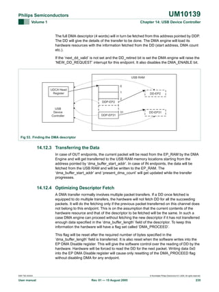
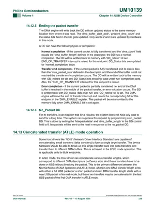
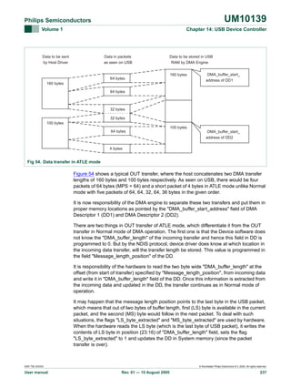
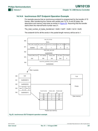
![UM10139
Philips Semiconductors
Volume 1
Chapter 15: TIMER0 and TIMER1
Table 237: TIMER/COUNTER0 and TIMER/COUNTER1 register map
Generic Description
Name
Access
Reset
value[1]
TIMER/
TIMER/
COUNTER0
COUNTER1
Address & Name Address & Name
IR
Interrupt Register. The IR can be written to clear
interrupts. The IR can be read to identify which of
eight possible interrupt sources are pending.
R/W
0
0xE000 4000
T0IR
0xE000 8000
T1IR
TCR
Timer Control Register. The TCR is used to control R/W
the Timer Counter functions. The Timer Counter can
be disabled or reset through the TCR.
0
0xE000 4004
T0TCR
0xE000 8004
T1TCR
TC
Timer Counter. The 32-bit TC is incremented every
PR+1 cycles of PCLK. The TC is controlled through
the TCR.
R/W
0
0xE000 4008
T0TC
0xE000 8008
T1TC
PR
Prescale Register. The Prescale Counter (below) is R/W
equal to this value, the next clock increments the TC
and clears the PC.
0
0xE000 400C
T0PR
0xE000 800C
T1PR
PC
Prescale Counter. The 32-bit PC is a counter which
is incremented to the value stored in PR. When the
value in PR is reached, the TC is incremented and
the PC is cleared. The PC is observable and
controllable through the bus interface.
R/W
0
0xE000 4010
T0PC
0xE000 8010
T1PC
MCR
Match Control Register. The MCR is used to control
if an interrupt is generated and if the TC is reset
when a Match occurs.
R/W
0
0xE0004014
T0MCR
0xE000 8014
T1MCR
MR0
Match Register 0. MR0 can be enabled through the
MCR to reset the TC, stop both the TC and PC,
and/or generate an interrupt every time MR0
matches the TC.
R/W
0
0xE000 4018
T0MR0
0xE000 8018
T1MR0
MR1
Match Register 1. See MR0 description.
R/W
0
0xE000 401C
T0MR1
0xE000 801C
T1MR1
MR2
Match Register 2. See MR0 description.
R/W
0
0xE000 4020
T0MR2
0xE000 8020
T1MR2
MR3
Match Register 3. See MR0 description.
R/W
0
0xE000 4024
T0MR3
0xE000 8024
T1MR3
CCR
Capture Control Register. The CCR controls which
R/W
edges of the capture inputs are used to load the
Capture Registers and whether or not an interrupt is
generated when a capture takes place.
0
0xE000 4028
T0CCR
0xE000 8028
T1CCR
CR0
Capture Register 0. CR0 is loaded with the value of RO
TC when there is an event on the CAPn.0(CAP0.0 or
CAP1.0 respectively) input.
0
0xE000 402C
T0CR0
0xE000 802C
T1CR0
CR1
Capture Register 1. See CR0 description.
RO
0
0xE000 4030
T0CR1
0xE000 8030
T1CR1
CR2
Capture Register 2. See CR0 description.
RO
0
0xE000 4034
T0CR2
0xE000 8034
T1CR2
© Koninklijke Philips Electronics N.V. 2005. All rights reserved.
User manual
Rev. 01 — 15 August 2005
244](https://image.slidesharecdn.com/armusrmanl-131212220701-phpapp02/85/Arm-usr-m-anl-244-320.jpg)
![UM10139
Philips Semiconductors
Volume 1
Chapter 15: TIMER0 and TIMER1
Table 237: TIMER/COUNTER0 and TIMER/COUNTER1 register map
Generic Description
Name
Access
Reset
value[1]
TIMER/
TIMER/
COUNTER0
COUNTER1
Address & Name Address & Name
CR3
Capture Register 3. See CR0 description.
RO
0
0xE000 4038
T0CR3
0xE000 8038
T1CR3
EMR
External Match Register. The EMR controls the
external match pins MATn.0-3 (MAT0.0-3 and
MAT1.0-3 respectively).
R/W
0
0xE000 403C
T0EMR
0xE000 803C
T1EMR
CTCR
Count Control Register. The CTCR selects between R/W
Timer and Counter mode, and in Counter mode
selects the signal and edge(s) for counting.
0
0xE000 4070
T0CTCR
0xE000 8070
T1CTCR
[1]
Reset value reflects the data stored in used bits only. It does not include reserved bits content.
15.5.1 Interrupt Register (IR, TIMER0: T0IR - 0xE000 4000 and TIMER1: T1IR
- 0xE000 8000)
The Interrupt Register consists of four bits for the match interrupts and four bits for the
capture interrupts. If an interrupt is generated then the corresponding bit in the IR will be
high. Otherwise, the bit will be low. Writing a logic one to the corresponding IR bit will reset
the interrupt. Writing a zero has no effect.
Table 238: Interrupt Register (IR, TIMER0: T0IR - address 0xE000 4000 and TIMER1: T1IR - address 0xE000 8000) bit
description
Bit
Symbol
Description
Reset value
0
MR0 Interrupt
Interrupt flag for match channel 0.
0
1
MR1 Interrupt
Interrupt flag for match channel 1.
0
2
MR2 Interrupt
Interrupt flag for match channel 2.
0
3
MR3 Interrupt
Interrupt flag for match channel 3.
0
4
CR0 Interrupt
Interrupt flag for capture channel 0 event.
0
5
CR1 Interrupt
Interrupt flag for capture channel 1 event.
0
6
CR2 Interrupt
Interrupt flag for capture channel 2 event.
0
7
CR3 Interrupt
Interrupt flag for capture channel 3 event.
0
15.5.2 Timer Control Register (TCR, TIMER0: T0TCR - 0xE000 4004 and
TIMER1: T1TCR - 0xE000 8004)
The Timer Control Register (TCR) is used to control the operation of the Timer/Counter.
© Koninklijke Philips Electronics N.V. 2005. All rights reserved.
User manual
Rev. 01 — 15 August 2005
245](https://image.slidesharecdn.com/armusrmanl-131212220701-phpapp02/85/Arm-usr-m-anl-245-320.jpg)
![UM10139
Philips Semiconductors
Volume 1
Chapter 15: TIMER0 and TIMER1
Table 239: Timer Control Register (TCR, TIMER0: T0TCR - address 0xE000 4004 and TIMER1:
T1TCR - address 0xE000 8004) bit description
Bit
Symbol
0
Counter Enable When one, the Timer Counter and Prescale Counter are 0
enabled for counting. When zero, the counters are
disabled.
Description
Reset value
1
Counter Reset
When one, the Timer Counter and the Prescale Counter 0
are synchronously reset on the next positive edge of
PCLK. The counters remain reset until TCR[1] is
returned to zero.
7:2
-
Reserved, user software should not write ones to
reserved bits. The value read from a reserved bit is not
defined.
NA
15.5.3 Count Control Register (CTCR, TIMER0: T0CTCR - 0xE000 4070 and
TIMER1: T1TCR - 0xE000 8070)
The Count Control Register (CTCR) is used to select between Timer and Counter mode,
and in Counter mode to select the pin and edge(s) for counting.
When Counter Mode is chosen as a mode of operation, the CAP input (selected by the
CTCR bits 3:2) is sampled on every rising edge of the PCLK clock. After comparing two
consecutive samples of this CAP input, one of the following four events is recognized:
rising edge, falling edge, either of edges or no changes in the level of the selected CAP
input. Only if the identified event corresponds to the one selected by bits 1:0 in the CTCR
register, the Timer Counter register will be incremented.
Effective processing of the externally supplied clock to the counter has some limitations.
Since two successive rising edges of the PCLK clock are used to identify only one edge
on the CAP selected input, the frequency of the CAP input can not exceed one half of the
PCLK clock. Consequently, duration of the high/low levels on the same CAP input in this
case can not be shorter than 1/PCLK.
Table 240: Count Control Register (CTCR, TIMER0: T0CTCR - address 0xE000 4070 and
TIMER1: T1TCR - address 0xE000 8070) bit description
Bit
Symbol
1:0
Value
Counter/
Timer
Mode
Description
Reset
value
This field selects which rising PCLK edges can increment
Timer’s Prescale Counter (PC), or clear PC and increment
Timer Counter (TC).
00
00
Timer Mode: every rising PCLK edge
01
Counter Mode: TC is incremented on rising edges on the
CAP input selected by bits 3:2.
10
Counter Mode: TC is incremented on falling edges on the
CAP input selected by bits 3:2.
11
Counter Mode: TC is incremented on both edges on the CAP
input selected by bits 3:2.
© Koninklijke Philips Electronics N.V. 2005. All rights reserved.
User manual
Rev. 01 — 15 August 2005
246](https://image.slidesharecdn.com/armusrmanl-131212220701-phpapp02/85/Arm-usr-m-anl-246-320.jpg)
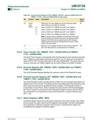
![UM10139
Philips Semiconductors
Volume 1
Chapter 15: TIMER0 and TIMER1
15.5.8 Match Control Register (MCR, TIMER0: T0MCR - 0xE000 4014 and
TIMER1: T1MCR - 0xE000 8014)
The Match Control Register is used to control what operations are performed when one of
the Match Registers matches the Timer Counter. The function of each of the bits is shown
in Table 241.
Table 241: Match Control Register (MCR, TIMER0: T0MCR - address 0xE000 4014 and TIMER1: T1MCR - address
0xE000 8014) bit description
Bit
Symbol
Value Description
Reset
value
0
MR0I
1
Interrupt on MR0: an interrupt is generated when MR0 matches the value in the TC.
0
0
This interrupt is disabled
1
Reset on MR0: the TC will be reset if MR0 matches it.
0
Feature disabled.
1
Stop on MR0: the TC and PC will be stopped and TCR[0] will be set to 0 if MR0 matches 0
the TC.
0
Feature disabled.
1
Interrupt on MR1: an interrupt is generated when MR1 matches the value in the TC.
0
This interrupt is disabled
1
Reset on MR1: the TC will be reset if MR1 matches it.
0
Feature disabled.
1
Stop on MR1: the TC and PC will be stopped and TCR[0] will be set to 0 if MR1 matches 0
the TC.
0
Feature disabled.
1
Interrupt on MR2: an interrupt is generated when MR2 matches the value in the TC.
0
This interrupt is disabled
1
Reset on MR2: the TC will be reset if MR2 matches it.
0
Feature disabled.
1
Stop on MR2: the TC and PC will be stopped and TCR[0] will be set to 0 if MR2 matches 0
the TC.
0
Feature disabled.
1
Interrupt on MR3: an interrupt is generated when MR3 matches the value in the TC.
0
This interrupt is disabled
1
Reset on MR3: the TC will be reset if MR3 matches it.
0
Feature disabled.
1
Stop on MR3: the TC and PC will be stopped and TCR[0] will be set to 0 if MR3 matches 0
the TC.
0
Feature disabled.
1
2
MR0R
MR0S
3
MR1I
4
MR1R
5
6
7
MR1S
MR2I
MR2R
8
MR2S
9
MR3I
10
MR3R
11
MR3S
15:12
-
0
0
0
0
0
0
0
Reserved, user software should not write ones to reserved bits. The value read from a
reserved bit is not defined.
NA
© Koninklijke Philips Electronics N.V. 2005. All rights reserved.
User manual
Rev. 01 — 15 August 2005
248](https://image.slidesharecdn.com/armusrmanl-131212220701-phpapp02/85/Arm-usr-m-anl-248-320.jpg)
![UM10139
Philips Semiconductors
Volume 1
Chapter 15: TIMER0 and TIMER1
Table 242: Capture Control Register (CCR, TIMER0: T0CCR - address 0xE000 4028 and TIMER1: T1CCR - address
0xE000 8028) bit description
Bit
Symbol
Value Description
Reset
value
10
CAP3FE
1
Capture on CAPn.3 falling edge: a sequence of 1 then 0 on CAPn.3 will cause CR3 to
be loaded with the contents of TC
0
0
This feature is disabled.
1
Interrupt on CAPn.3 event: a CR3 load due to a CAPn.3 event will generate an interrupt. 0
0
This feature is disabled.
11
CAP3I
15:12 -
Reserved, user software should not write ones to reserved bits. The value read from a
reserved bit is not defined.
NA
15.5.11 External Match Register (EMR, TIMER0: T0EMR - 0xE000 403C; and
TIMER1: T1EMR - 0xE000 803C)
The External Match Register provides both control and status of the external match pins
MAT(0-3).
Table 243: External Match Register (EMR, TIMER0: T0EMR - address 0xE000 403C and TIMER1: T1EMR address0xE000 803C) bit description
Bit
Symbol
Description
Reset
value
0
EM0
External Match 0. This bit reflects the state of output MAT0.0/MAT1.0, whether or not this 0
output is connected to its pin. When a match occurs between the TC and MR0, this output
of the timer can either toggle, go low, go high, or do nothing. Bits EMR[5:4] control the
functionality of this output.
1
EM1
External Match 1. This bit reflects the state of output MAT0.1/MAT1.1, whether or not this 0
output is connected to its pin. When a match occurs between the TC and MR1, this output
of the timer can either toggle, go low, go high, or do nothing. Bits EMR[7:6] control the
functionality of this output.
2
EM2
External Match 2. This bit reflects the state of output MAT0.2/MAT1.2, whether or not this 0
output is connected to its pin. When a match occurs between the TC and MR2, this output
of the timer can either toggle, go low, go high, or do nothing. Bits EMR[9:8] control the
functionality of this output.
3
EM3
External Match 3. This bit reflects the state of output MAT0.3/MAT1.3, whether or not this 0
output is connected to its pin. When a match occurs between the TC and MR3, this output
of the timer can either toggle, go low, go high, or do nothing. Bits EMR[11:10] control the
functionality of this output.
5:4
EMC0
External Match Control 0. Determines the functionality of External Match 0. Table 244
shows the encoding of these bits.
00
7:6
EMC1
External Match Control 1. Determines the functionality of External Match 1. Table 244
shows the encoding of these bits.
00
9:8
EMC2
External Match Control 2. Determines the functionality of External Match 2. Table 244
shows the encoding of these bits.
00
11:10
EMC3
External Match Control 3. Determines the functionality of External Match 3. Table 244
shows the encoding of these bits.
00
15:12
-
Reserved, user software should not write ones to reserved bits. The value read from a
reserved bit is not defined.
NA
© Koninklijke Philips Electronics N.V. 2005. All rights reserved.
User manual
Rev. 01 — 15 August 2005
250](https://image.slidesharecdn.com/armusrmanl-131212220701-phpapp02/85/Arm-usr-m-anl-250-320.jpg)
![UM10139
Philips Semiconductors
Volume 1
Chapter 15: TIMER0 and TIMER1
Table 244: External match control
EMR[11:10], EMR[9:8],
EMR[7:6], or EMR[5:4]
Function
00
Do Nothing.
01
Clear the corresponding External Match bit/output to 0 (MATn.m pin is LOW if pinned out).
10
Set the corresponding External Match bit/output to 1 (MATn.m pin is HIGH if pinned out).
11
Toggle the corresponding External Match bit/output.
15.6 Example timer operation
Figure 56 shows a timer configured to reset the count and generate an interrupt on match.
The prescaler is set to 2 and the match register set to 6. At the end of the timer cycle
where the match occurs, the timer count is reset. This gives a full length cycle to the
match value. The interrupt indicating that a match occurred is generated in the next clock
after the timer reached the match value.
Figure 57 shows a timer configured to stop and generate an interrupt on match. The
prescaler is again set to 2 and the match register set to 6. In the next clock after the timer
reaches the match value, the timer enable bit in TCR is cleared, and the interrupt
indicating that a match occurred is generated.
PCLK
Prescale
counter
Timer
counter
2
0
1
4
2
0
1
5
2
6
0
1
0
2
0
1
1
Timer counter
reset
Iterrupt
Fig 56. A timer cycle in which PR=2, MRx=6, and both interrupt and reset on match are enabled
PCLK
Prescale
counter
Timer
counter
TCR[0]
(counter enable)
2
4
0
1
5
1
2
0
6
0
Iterrupt
Fig 57. A timer cycle in which PR=2, MRx=6, and both interrupt and stop on match are enabled
© Koninklijke Philips Electronics N.V. 2005. All rights reserved.
User manual
Rev. 01 — 15 August 2005
251](https://image.slidesharecdn.com/armusrmanl-131212220701-phpapp02/85/Arm-usr-m-anl-251-320.jpg)
![UM10139
Philips Semiconductors
Volume 1
Chapter 15: TIMER0 and TIMER1
15.7 Architecture
The block diagram for TIMER/COUNTER0 and TIMER/COUNTER1 is shown in
Figure 58.
MATCH REGISTER 0
MATCH REGISTER 1
MATCH REGISTER 2
MATCH REGISTER 3
MATCH CONTROL REGISTER
EXTERNAL MATCH REGISTER
INTRRUPT REGISTER
CONTROL
=
MAT[3:0]
INTERRUPT
=
CAP[3:0]
=
STOP ON MATCH
RESET ON MATCH
=
LOAD[3:0]
CAPTURE CONTROL REGISTER
CSN
CAPTURE REGISTER 0
TIMER COUNTER
CAPTURE REGISTER 1
CE
CAPTURE REGISTER 2
CAPTURE REGISTER 3*
TCI
PRESCALE COUNTER
RESET
ENABLE
TIMER CONTROL REGISTER
PCLK
MAXVAL
PRESCALE REGISTER
* Note: that the capture register 3 cannot be used on TIMER0
Fig 58. Timer block diagram
© Koninklijke Philips Electronics N.V. 2005. All rights reserved.
User manual
Rev. 01 — 15 August 2005
252](https://image.slidesharecdn.com/armusrmanl-131212220701-phpapp02/85/Arm-usr-m-anl-252-320.jpg)
![UM10139
Philips Semiconductors
Volume 1
Chapter 16: PWM
MATCH REGISTER 0
SHADOW REGISTER 0
LOAD ENABLE
MATCH REGISTER 1
SHADOW REGISTER 1
LOAD ENABLE
MATCH REGISTER 2
SHADOW REGISTER 2
LOAD ENABLE
MATCH REGISTER 3
SHADOW REGISTER 3
LOAD ENABLE
MATCH REGISTER 4
SHADOW REGISTER 4
LOAD ENABLE
MATCH REGISTER 5
SHADOW REGISTER 5
LOAD ENABLE
MATCH REGISTER 6
SHADOW REGISTER 6
LOAD ENABLE
Match 0
PWM1
S
Q
R
EN
Match 1
PWMENA1
MATCH 0
PWMSEL2
LATCH ENABLE REGISTER
PWM2
CLEAR
MUX
S
Q
R
EN
Match 2
MATCH CONTROL REGISTER
PWMENA2
=
Interrupt Register
PWMSEL3
=
PWM3
MUX
=
M[6.0]
S
Q
R
CONTROL
EN
Match 3
PWMENA3
INTERRUPT
=
PWMSEL4
STOP ON MATCH
RESET ON MATCH
PWM4
=
MUX
CSN
Q
R
=
S
EN
Match 4
PWMENA4
=
PWMSEL5
PWM5
MUX
S
Q
R
EN
Match 5
PWMENA5
TIMER COUNTER
PWMSEL6
CE
MUX
PWM6
S
Q
R
EN
TCI
Match 6
PRESCALE COUNTER
ENABLE
PWMENA1..6
PWMENA6
PWMSEL2..6
MAXVAL
RESET
TIMER CONTROL REGISTER
PRESCALE REGISTER
PWM CONTROL REGISTER
Note: this diagram is intended to clarify the function of the PWM rather than to suggest a specific design implementation.
Fig 59. PWM block diagram
© Koninklijke Philips Electronics N.V. 2005. All rights reserved.
User manual
Rev. 01 — 15 August 2005
255](https://image.slidesharecdn.com/armusrmanl-131212220701-phpapp02/85/Arm-usr-m-anl-255-320.jpg)
![UM10139
Philips Semiconductors
Volume 1
Chapter 16: PWM
A sample of how PWM values relate to waveform outputs is shown in Figure 60. PWM
output logic is shown in Figure 59 that allows selection of either single or double edge
controlled PWM outputs via the muxes controlled by the PWMSELn bits. The match
register selections for various PWM outputs is shown in Table 245. This implementation
supports up to N-1 single edge PWM outputs or (N-1)/2 double edge PWM outputs, where
N is the number of match registers that are implemented. PWM types can be mixed if
desired.
The waveforms below show a single PWM cycle and demonstrate PWM outputs under the
following conditions:
The timer is configured for PWM mode.
The match register values are as follows:
Match 0 is configured to reset the timer/counter
MRO = 100 (PWM rate)
when a match event occurs.
MR1 = 41, MR2 = 78 (PWM2 output)
Control bits PWMSEL2 and PWMSEL4 are set.
MR3 = 53, MR4 = 27 (PWM4 output)
MR5 = 65 (PWM5 output)
PWM2
PWM4
PWM5
0
27
41
53
65
78
100
(counter is reset)
Fig 60. Sample PWM waveforms
Table 245: Set and reset inputs for PWM Flip-Flops
PWM Channel
Single Edge PWM (PWMSELn = 0)
Double Edge PWM (PWMSELn = 1)
Set by
Set by
Reset by
Reset by
0[1]
1
Match 0
Match 1
Match
2
Match 0
Match 2
Match 1
2[2]
3
Match 0
Match 3
Match
4
Match 0
Match 4
Match 3
4[2]
5
Match 0
Match 5
Match
6
Match 0
Match 6
Match 5
Match 1[1]
Match 2
Match 3[2]
Match 4
Match 5[2]
Match 6
[1]
Identical to single edge mode in this case since Match 0 is the neighboring match register. Essentially,
PWM1 cannot be a double edged output.
[2]
It is generally not advantageous to use PWM channels 3 and 5 for double edge PWM outputs because it
would reduce the number of double edge PWM outputs that are possible. Using PWM 2, PWM4, and
PWM6 for double edge PWM outputs provides the most pairings.
16.2.1 Rules for single edge controlled PWM outputs
1. All single edge controlled PWM outputs go high at the beginning of a PWM cycle
unless their match value is equal to 0.
© Koninklijke Philips Electronics N.V. 2005. All rights reserved.
User manual
Rev. 01 — 15 August 2005
256](https://image.slidesharecdn.com/armusrmanl-131212220701-phpapp02/85/Arm-usr-m-anl-256-320.jpg)
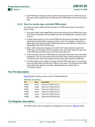
![UM10139
Philips Semiconductors
Volume 1
Chapter 16: PWM
Table 247: Pulse Width Modulator (PWM) register map
Name
Description
Access
Reset
value[1]
Address
PWMIR
PWM Interrupt Register. The PWMIR can be written to clear interrupts.
The PWMIR can be read to identify which of the possible interrupt
sources are pending.
R/W
0
0xE001 4000
PWMTCR PWM Timer Control Register. The PWMTCR is used to control the Timer R/W
Counter functions. The Timer Counter can be disabled or reset through
the PWMTCR.
0
0xE001 4004
PWMTC
PWM Timer Counter. The 32-bit TC is incremented every PWMPR+1
cycles of PCLK. The PWMTC is controlled through the PWMTCR.
R/W
0
0xE001 4008
PWMPR
PWM Prescale Register. The PWMTC is incremented every PWMPR+1
cycles of PCLK.
R/W
0
0xE001 400C
PWMPC
PWM Prescale Counter. The 32-bit PC is a counter which is incremented R/W
to the value stored in PR. When the value in PWMPR is reached, the
PWMTC is incremented. The PWMPC is observable and controllable
through the bus interface.
0
0xE001 4010
R/W
0
0xE001 4014
PWMMR0 PWM Match Register 0. PWMMR0 can be enabled through PWMMCR to R/W
reset the PWMTC, stop both the PWMTC and PWMPC, and/or generate
an interrupt when it matches the PWMTC. In addition, a match between
PWMMR0 and the PWMTC sets all PWM outputs that are in single-edge
mode, and sets PWM1 if it is in double-edge mode.
0
0xE001 4018
PWMMR1 PWM Match Register 1. PWMMR1 can be enabled through PWMMCR to R/W
reset the PWMTC, stop both the PWMTC and PWMPC, and/or generate
an interrupt when it matches the PWMTC. In addition, a match between
PWMMR1 and the PWMTC clears PWM1 in either single-edge mode or
double-edge mode, and sets PWM2 if it is in double-edge mode.
0
0xE001 401C
PWMMR2 PWM Match Register 2. PWMMR2 can be enabled through PWMMCR to R/W
reset the PWMTC, stop both the PWMTC and PWMPC, and/or generate
an interrupt when it matches the PWMTC. In addition, a match between
PWMMR2 and the PWMTC clears PWM2 in either single-edge mode or
double-edge mode, and sets PWM3 if it is in double-edge mode.
0
0xE001 4020
PWMMR3 PWM Match Register 3. PWMMR3 can be enabled through PWMMCR to R/W
reset the PWMTC, stop both the PWMTC and PWMPC, and/or generate
an interrupt when it matches the PWMTC. In addition, a match between
PWMMR3 and the PWMTC clears PWM3 in either single-edge mode or
double-edge mode, and sets PWM4 if it is in double-edge mode.
0
0xE001 4024
PWMMR4 PWM Match Register 4. PWMMR4 can be enabled through PWMMCR to R/W
reset the PWMTC, stop both the PWMTC and PWMPC, and/or generate
an interrupt when it matches the PWMTC. In addition, a match between
PWMMR4 and the PWMTC clears PWM4 in either single-edge mode or
double-edge mode, and sets PWM5 if it is in double-edge mode.
0
0xE001 4040
PWMMR5 PWM Match Register 5. PWMMR5 can be enabled through PWMMCR to R/W
reset the PWMTC, stop both the PWMTC and PWMPC, and/or generate
an interrupt when it matches the PWMTC. In addition, a match between
PWMMR5 and the PWMTC clears PWM5 in either single-edge mode or
double-edge mode, and sets PWM6 if it is in double-edge mode.
0
0xE001 4044
PWMMCR PWM Match Control Register. The PWMMCR is used to control if an
interrupt is generated and if the PWMTC is reset when a Match occurs.
© Koninklijke Philips Electronics N.V. 2005. All rights reserved.
User manual
Rev. 01 — 15 August 2005
258](https://image.slidesharecdn.com/armusrmanl-131212220701-phpapp02/85/Arm-usr-m-anl-258-320.jpg)
![UM10139
Philips Semiconductors
Volume 1
Chapter 16: PWM
Table 247: Pulse Width Modulator (PWM) register map
Name
Description
Access
Reset
value[1]
Address
PWMMR6 PWM Match Register 6. PWMMR6 can be enabled through PWMMCR to R/W
reset the PWMTC, stop both the PWMTC and PWMPC, and/or generate
an interrupt when it matches the PWMTC. In addition, a match between
PWMMR6 and the PWMTC clears PWM6 in either single-edge mode or
double-edge mode.
0
0xE001 4048
PWMPCR PWM Control Register. Enables PWM outputs and selects PWM channel R/W
types as either single edge or double edge controlled.
0
0xE001 404C
PWMLER
0
0xE001 4050
PWM Latch Enable Register. Enables use of new PWM match values.
[1]
R/W
Reset value reflects the data stored in used bits only. It does not include reserved bits content.
16.4.1 PWM Interrupt Register (PWMIR - 0xE001 4000)
The PWM Interrupt Register consists of eleven bits (Table 248), seven for the match
interrupts and four reserved for the future use. If an interrupt is generated then the
corresponding bit in the PWMIR will be high. Otherwise, the bit will be low. Writing a logic
one to the corresponding IR bit will reset the interrupt. Writing a zero has no effect.
Table 248: PWM Interrupt Register (PWMIR - address 0xE001 4000) bit description
Bit
Symbol
Description
Reset value
0
PWMMR0 Interrupt
Interrupt flag for PWM match channel 0.
0
1
PWMMR1 Interrupt
Interrupt flag for PWM match channel 1.
0
2
PWMMR2 Interrupt
Interrupt flag for PWM match channel 2.
0
3
PWMMR3 Interrupt
Interrupt flag for PWM match channel 3.
0
7:4
-
Reserved, user software should not write ones to reserved bits.
The value read from a reserved bit is not defined.
0000
8
PWMMR4 Interrupt
Interrupt flag for PWM match channel 4.
0
9
PWMMR5 Interrupt
Interrupt flag for PWM match channel 5.
0
10
PWMMR6 Interrupt
Interrupt flag for PWM match channel 6.
0
15:11
-
Reserved, user software should not write ones to reserved bits.
The value read from a reserved bit is not defined.
NA
16.4.2 PWM Timer Control Register (PWMTCR - 0xE001 4004)
The PWM Timer Control Register (PWMTCR) is used to control the operation of the PWM
Timer Counter. The function of each of the bits is shown in Table 249.
© Koninklijke Philips Electronics N.V. 2005. All rights reserved.
User manual
Rev. 01 — 15 August 2005
259](https://image.slidesharecdn.com/armusrmanl-131212220701-phpapp02/85/Arm-usr-m-anl-259-320.jpg)
![UM10139
Philips Semiconductors
Volume 1
Chapter 16: PWM
Table 249: PWM Timer Control Register (PWMTCR - address 0xE001 4004) bit description
Bit
Symbol
Description
Reset value
0
Counter Enable When one, the PWM Timer Counter and PWM Prescale 0
Counter are enabled for counting. When zero, the
counters are disabled.
1
Counter Reset
When one, the PWM Timer Counter and the PWM
Prescale Counter are synchronously reset on the next
positive edge of PCLK. The counters remain reset until
TCR[1] is returned to zero.
0
2
-
Reserved, user software should not write ones to
reserved bits. The value read from a reserved bit is not
defined.
NA
3
PWM Enable
When one, PWM mode is enabled. PWM mode causes 0
shadow registers to operate in connection with the
Match registers. A program write to a Match register will
not have an effect on the Match result until the
corresponding bit in PWMLER has been set, followed by
the occurrence of a PWM Match 0 event. Note that the
PWM Match register that determines the PWM rate
(PWM Match 0) must be set up prior to the PWM being
enabled. Otherwise a Match event will not occur to
cause shadow register contents to become effective.
7:4
-
Reserved, user software should not write ones to
reserved bits. The value read from a reserved bit is not
defined.
NA
16.4.3 PWM Timer Counter (PWMTC - 0xE001 4008)
The 32-bit PWM Timer Counter is incremented when the Prescale Counter reaches its
terminal count. Unless it is reset before reaching its upper limit, the PWMTC will count up
through the value 0xFFFF FFFF and then wrap back to the value 0x0000 0000. This event
does not cause an interrupt, but a Match register can be used to detect an overflow if
needed.
16.4.4 PWM Prescale Register (PWMPR - 0xE001 400C)
The 32-bit PWM Prescale Register specifies the maximum value for the PWM Prescale
Counter.
16.4.5 PWM Prescale Counter register (PWMPC - 0xE001 4010)
The 32-bit PWM Prescale Counter controls division of PCLK by some constant value
before it is applied to the PWM Timer Counter. This allows control of the relationship of the
resolution of the timer versus the maximum time before the timer overflows. The PWM
Prescale Counter is incremented on every PCLK. When it reaches the value stored in the
PWM Prescale Register, the PWM Timer Counter is incremented and the PWM Prescale
Counter is reset on the next PCLK. This causes the PWM TC to increment on every PCLK
when PWMPR = 0, every 2 PCLKs when PWMPR = 1, etc.
© Koninklijke Philips Electronics N.V. 2005. All rights reserved.
User manual
Rev. 01 — 15 August 2005
260](https://image.slidesharecdn.com/armusrmanl-131212220701-phpapp02/85/Arm-usr-m-anl-260-320.jpg)
![UM10139
Philips Semiconductors
Volume 1
Chapter 16: PWM
16.4.6 PWM Match Registers (PWMMR0 - PWMMR6)
The 32-bit PWM Match register values are continuously compared to the PWM Timer
Counter value. When the two values are equal, actions can be triggered automatically.
The action possibilities are to generate an interrupt, reset the PWM Timer Counter, or stop
the timer. Actions are controlled by the settings in the PWMMCR register.
16.4.7 PWM Match Control Register (PWMMCR - 0xE001 4014)
The PWM Match Control Register is used to control what operations are performed when
one of the PWM Match Registers matches the PWM Timer Counter. The function of each
of the bits is shown in Table 250.
Table 250: Match Control Register (MCR, TIMER0: T0MCR - address 0xE000 4014 and TIMER1: T1MCR - address
0xE000 8014) bit description
Bit
Symbol
Value
Description
0
PWMMR0I
1
Interrupt on PWMMR0: an interrupt is generated when PWMMR0 matches the value 0
in the PWMTC.
0
This interrupt is disabled.
1
PWMMR0R 1
0
2
PWMMR0S 1
Reset
value
Reset on PWMMR0: the PWMTC will be reset if PWMMR0 matches it.
0
This feature is disabled.
Stop on PWMMR0: the PWMTC and PWMPC will be stopped and PWMTCR[0] will
be set to 0 if PWMMR0 matches the PWMTC.
0
0
This feature is disabled
1
Interrupt on PWMMR1: an interrupt is generated when PWMMR1 matches the value 0
in the PWMTC.
0
This interrupt is disabled.
3
PWMMR1I
1
PWMMR1R 1
0
5
PWMMR1S 1
Reset on PWMMR1: the PWMTC will be reset if PWMMR1 matches it.
0
This feature is disabled.
Stop on PWMMR1: the PWMTC and PWMPC will be stopped and PWMTCR[0] will
be set to 0 if PWMMR1 matches the PWMTC.
0
0
This feature is disabled.
1
Interrupt on PWMMR2: an interrupt is generated when PWMMR2 matches the value 0
in the PWMTC.
0
This interrupt is disabled.
6
PWMMR2I
7
PWMMR2R 1
0
8
PWMMR2S 1
Reset on PWMMR2: the PWMTC will be reset if PWMMR2 matches it.
0
This feature is disabled.
Stop on PWMMR2: the PWMTC and PWMPC will be stopped and PWMTCR[0] will
be set to 0 if PWMMR2 matches the PWMTC.
0
0
This feature is disabled
1
Interrupt on PWMMR3: an interrupt is generated when PWMMR3 matches the value 0
in the PWMTC.
0
This interrupt is disabled.
9
PWMMR3I
10
PWMMR3R 1
0
Reset on PWMMR3: the PWMTC will be reset if PWMMR3 matches it.
0
This feature is disabled
© Koninklijke Philips Electronics N.V. 2005. All rights reserved.
User manual
Rev. 01 — 15 August 2005
261](https://image.slidesharecdn.com/armusrmanl-131212220701-phpapp02/85/Arm-usr-m-anl-261-320.jpg)
![UM10139
Philips Semiconductors
Volume 1
Chapter 16: PWM
Table 250: Match Control Register (MCR, TIMER0: T0MCR - address 0xE000 4014 and TIMER1: T1MCR - address
0xE000 8014) bit description
Bit
Symbol
Value
11
PWMMR3S 1
Description
Reset
value
Stop on PWMMR3: The PWMTC and PWMPC will be stopped and PWMTCR[0] will
be set to 0 if PWMMR3 matches the PWMTC.
0
0
13
PWMMR4I
1
Interrupt on PWMMR4: An interrupt is generated when PWMMR4 matches the value 0
in the PWMTC.
0
12
This feature is disabled
This interrupt is disabled.
PWMMR4R 1
Reset on PWMMR4: the PWMTC will be reset if PWMMR4 matches it.
0
14
0
This feature is disabled.
PWMMR4S 1
Stop on PWMMR4: the PWMTC and PWMPC will be stopped and PWMTCR[0] will
be set to 0 if PWMMR4 matches the PWMTC.
0
0
16
PWMMR5I
1
Interrupt on PWMMR5: An interrupt is generated when PWMMR5 matches the value 0
in the PWMTC.
0
15
This feature is disabled
This interrupt is disabled.
PWMMR5R 1
Reset on PWMMR5: the PWMTC will be reset if PWMMR5 matches it.
0
17
0
This feature is disabled.
PWMMR5S 1
Stop on PWMMR5: the PWMTC and PWMPC will be stopped and PWMTCR[0] will
be set to 0 if PWMMR5 matches the PWMTC.
0
0
19
PWMMR6I
1
Interrupt on PWMMR6: an interrupt is generated when PWMMR6 matches the value 0
in the PWMTC.
0
18
This feature is disabled
This interrupt is disabled.
PWMMR6R 1
Reset on PWMMR6: the PWMTC will be reset if PWMMR6 matches it.
0
20
0
This feature is disabled.
PWMMR6S 1
Stop on PWMMR6: the PWMTC and PWMPC will be stopped and PWMTCR[0] will
be set to 0 if PWMMR6 matches the PWMTC.
0
0
This feature is disabled
31:21 -
Reserved, user software should not write ones to reserved bits. The value read from
a reserved bit is not defined.
NA
16.4.8 PWM Control Register (PWMPCR - 0xE001 404C)
The PWM Control Register is used to enable and select the type of each PWM channel.
The function of each of the bits are shown in Table 251.
Table 251: PWM Control Register (PWMPCR - address 0xE001 404C) bit description
Bit
Symbol
1:0
-
2
PWMSEL2
Reset
value
Reserved, user software should not write ones to reserved bits. The value read from
a reserved bit is not defined.
NA
1
Selects double edge controlled mode for the PWM2 output.
0
Selects single edge controlled mode for PWM2.
1
Selects double edge controlled mode for the PWM3 output.
0
PWMSEL3
Description
0
3
Value
Selects single edge controlled mode for PWM3.
0
© Koninklijke Philips Electronics N.V. 2005. All rights reserved.
User manual
Rev. 01 — 15 August 2005
262](https://image.slidesharecdn.com/armusrmanl-131212220701-phpapp02/85/Arm-usr-m-anl-262-320.jpg)
![UM10139
Philips Semiconductors
Volume 1
Chapter 17: A/D Converter
17.4 Register description
The A/D Converter registers are shown in Table 254.
Table 254: ADC registers
Generic
Name
Description
Access Reset
value[1]
AD0
Address
& Name
AD1
Address
& Name
ADCR
A/D Control Register. The ADCR register must be
written to select the operating mode before A/D
conversion can occur.
R/W
0x0000 0001 0xE003 4000 0xE006 0000
AD0CR
AD1CR
ADGDR
A/D Global Data Register. This register contains the
ADC’s DONE bit and the result of the most recent A/D
conversion.
R/W
NA
ADSTAT
A/D Status Register. This register contains DONE and
OVERRUN flags for all of the A/D channels, as well as
the A/D interrupt flag.
RO
0x0000 0000 0xE003 4030 0xE006 0030
AD0STAT
AD1STAT
ADGSR
A/D Global Start Register. This address can be written
(in the AD0 address range) to start conversions in both
A/D converters simultaneously.
WO
0x00
ADINTEN A/D Interrupt Enable Register. This register contains
enable bits that allow the DONE flag of each A/D
channel to be included or excluded from contributing to
the generation of an A/D interrupt.
R/W
0x0000 0100 0xE003 400C 0xE006 000C
AD0INTEN
AD1INTEN
0xE003 4004 0xE006 0004
AD0GDR
AD1GDR
0xE003 4008
ADGSR
ADDR0
A/D Channel 0 Data Register. This register contains the RO
result of the most recent conversion completed on
channel 0.
NA
0xE003 4010 0xE006 0010
AD0DR0
AD1DR0
ADDR1
A/D Channel 1 Data Register. This register contains the RO
result of the most recent conversion completed on
channel 1.
NA
0xE003 4014 0xE006 0014
AD0DR1
AD1DR1
ADDR2
A/D Channel 2 Data Register. This register contains the RO
result of the most recent conversion completed on
channel 2.
NA
0xE003 4018 0xE006 0018
AD0DR2
AD1DR2
ADDR3
A/D Channel 3 Data Register. This register contains the RO
result of the most recent conversion completed on
channel 3.
NA
0xE003 401C 0xE006 001C
AD0DR3
AD1DR3
ADDR4
A/D Channel 4 Data Register. This register contains the RO
result of the most recent conversion completed on
channel 4.
NA
0xE003 4020 0xE006 0020
AD0DR4
AD1DR4
ADDR5
A/D Channel 5 Data Register. This register contains the RO
result of the most recent conversion completed on
channel 5.
NA
0xE003 4024 0xE006 0024
AD0DR5
AD1DR5
ADDR6
A/D Channel 6 Data Register. This register contains the RO
result of the most recent conversion completed on
channel 6.
NA
0xE003 4028 0xE006 0028
AD0DR6
AD1DR6
ADDR7
A/D Channel 7 Data Register. This register contains the RO
result of the most recent conversion completed on
channel 7.
NA
0xE003 402C 0xE006 002C
AD0DR7
AD1DR7
[1]
Reset value reflects the data stored in used bits only. It does not include reserved bits content.
© Koninklijke Philips Electronics N.V. 2005. All rights reserved.
User manual
Rev. 01 — 15 August 2005
266](https://image.slidesharecdn.com/armusrmanl-131212220701-phpapp02/85/Arm-usr-m-anl-266-320.jpg)
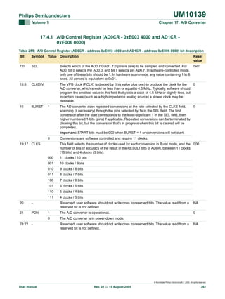
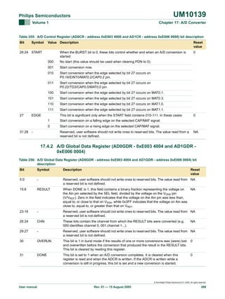
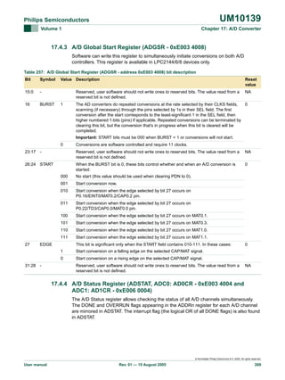
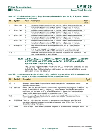
![UM10139
Philips Semiconductors
Volume 1
Chapter 19: RTC
19.4 Register description
The RTC includes a number of registers. The address space is split into four sections by
functionality. The first eight addresses are the Miscellaneous Register Group
(Section 19.4.2). The second set of eight locations are the Time Counter Group
(Section 19.4.12). The third set of eight locations contain the Alarm Register Group
(Section 19.4.14). The remaining registers control the Reference Clock Divider.
The Real Time Clock includes the register shown in Table 263. Detailed descriptions of
the registers follow.
Table 263: Real Time Clock (RTC) register map
Name
Size Description
Access
Reset
value[1]
Address
ILR
2
Interrupt Location Register
R/W
*
0xE002 4000
CTC
15
Clock Tick Counter
RO
*
0xE002 4004
CCR
4
Clock Control Register
R/W
*
0xE002 4008
CIIR
8
Counter Increment Interrupt Register
R/W
*
0xE002 400C
AMR
8
Alarm Mask Register
R/W
*
0xE002 4010
CTIME0
32
Consolidated Time Register 0
RO
*
0xE002 4014
CTIME1
32
Consolidated Time Register 1
RO
*
0xE002 4018
CTIME2
32
Consolidated Time Register 2
RO
*
0xE002 401C
SEC
6
Seconds Counter
R/W
*
0xE002 4020
MIN
6
Minutes Register
R/W
*
0xE002 4024
HOUR
5
Hours Register
R/W
*
0xE002 4028
DOM
5
Day of Month Register
R/W
*
0xE002 402C
DOW
3
Day of Week Register
R/W
*
0xE002 4030
DOY
9
Day of Year Register
R/W
*
0xE002 4034
MONTH
4
Months Register
R/W
*
0xE002 4038
YEAR
12
Years Register
R/W
*
0xE002 403C
ALSEC
6
Alarm value for Seconds
R/W
*
0xE002 4060
ALMIN
6
Alarm value for Minutes
R/W
*
0xE002 4064
ALHOUR
5
Alarm value for Seconds
R/W
*
0xE002 4068
ALDOM
5
Alarm value for Day of Month
R/W
*
0xE002 406C
ALDOW
3
Alarm value for Day of Week
R/W
*
0xE002 4070
ALDOY
9
Alarm value for Day of Year
R/W
*
0xE002 4074
ALMON
4
Alarm value for Months
R/W
*
0xE002 4078
ALYEAR
12
Alarm value for Year
R/W
*
0xE002 407C
PREINT
13
Prescaler value, integer portion
R/W
0
0xE002 4080
PREFRAC 15
Prescaler value, integer portion
R/W
0
0xE002 4084
[1]
Registers in the RTC other than those that are part of the Prescaler are not affected by chip Reset. These
registers must be initialized by software if the RTC is enabled. Reset value reflects the data stored in used
bits only. It does not include reserved bits content.
© Koninklijke Philips Electronics N.V. 2005. All rights reserved.
User manual
Rev. 01 — 15 August 2005
276](https://image.slidesharecdn.com/armusrmanl-131212220701-phpapp02/85/Arm-usr-m-anl-276-320.jpg)
![UM10139
Philips Semiconductors
Volume 1
Chapter 19: RTC
19.4.1 RTC interrupts
Interrupt generation is controlled through the Interrupt Location Register (ILR), Counter
Increment Interrupt Register (CIIR), the alarm registers, and the Alarm Mask Register
(AMR). Interrupts are generated only by the transition into the interrupt state. The ILR
separately enables CIIR and AMR interrupts. Each bit in CIIR corresponds to one of the
time counters. If CIIR is enabled for a particular counter, then every time the counter is
incremented an interrupt is generated. The alarm registers allow the user to specify a date
and time for an interrupt to be generated. The AMR provides a mechanism to mask alarm
compares. If all nonmasked alarm registers match the value in their corresponding time
counter, then an interrupt is generated.
The RTC interrupt can bring the microcontroller out of power-down mode if the RTC is
operating from its own oscillator on the RTCX1-2 pins. When the RTC interrupt is enabled
for wakeup and its selected event occurs, XTAL1/2 pins associated oscillator wakeup
cycle is started. For details on the RTC based wakeup process see Section 3.5.3
“Interrupt Wakeup register (INTWAKE - 0xE01F C144)” on page 22 and Section 3.12
“Wakeup timer” on page 41.
19.4.2 Miscellaneous register group
Table 264 summarizes the registers located from 0 to 7 of A[6:2]. More detailed
descriptions follow.
Table 264: Miscellaneous registers
Name
Size Description
Access
ILR
2
Interrupt Location. Reading this location
R/W
indicates the source of an interrupt. Writing a
one to the appropriate bit at this location clears
the associated interrupt.
0xE002 4000
CTC
15
Clock Tick Counter. Value from the clock
divider.
0xE002 4004
CCR
4
Clock Control Register. Controls the function of R/W
the clock divider.
0xE002 4008
CIIR
8
Counter Increment Interrupt. Selects which
counters will generate an interrupt when they
are incremented.
R/W
0xE002 400C
AMR
8
Alarm Mask Register. Controls which of the
alarm registers are masked.
R/W
0xE002 4010
CTIME0
32
Consolidated Time Register 0
RO
0xE002 4014
CTIME1
32
Consolidated Time Register 1
RO
0xE002 4018
CTIME2
32
Consolidated Time Register 2
RO
0xE002 401C
RO
Address
19.4.3 Interrupt Location Register (ILR - 0xE002 4000)
The Interrupt Location Register is a 2-bit register that specifies which blocks are
generating an interrupt (see Table 265). Writing a one to the appropriate bit clears the
corresponding interrupt. Writing a zero has no effect. This allows the programmer to read
this register and write back the same value to clear only the interrupt that is detected by
the read.
© Koninklijke Philips Electronics N.V. 2005. All rights reserved.
User manual
Rev. 01 — 15 August 2005
277](https://image.slidesharecdn.com/armusrmanl-131212220701-phpapp02/85/Arm-usr-m-anl-277-320.jpg)
![UM10139
Philips Semiconductors
Volume 1
Chapter 19: RTC
Table 265: Interrupt Location Register (ILR - address 0xE002 4000) bit description
Bit
Symbol
Description
Reset
value
0
RTCCIF
When one, the Counter Increment Interrupt block generated an interrupt. NA
Writing a one to this bit location clears the counter increment interrupt.
1
RTCALF
When one, the alarm registers generated an interrupt. Writing a one to
this bit location clears the alarm interrupt.
NA
7:2
-
Reserved, user software should not write ones to reserved bits. The
value read from a reserved bit is not defined.
NA
19.4.4 Clock Tick Counter Register (CTCR - 0xE002 4004)
The Clock Tick Counter is read only. It can be reset to zero through the Clock Control
Register (CCR). The CTC consists of the bits of the clock divider counter.
Table 266: Clock Tick Counter Register (CTCR - address 0xE002 4004) bit description
Bit
Symbol
Description
Reset
value
14:0
Clock Tick Prior to the Seconds counter, the CTC counts 32,768 clocks per
NA
Counter
second. Due to the RTC Prescaler, these 32,768 time increments may
not all be of the same duration. Refer to the Section 19.6 “Reference
clock divider (prescaler)” on page 282 for details.
15
-
Reserved, user software should not write ones to reserved bits. The
value read from a reserved bit is not defined.
NA
19.4.5 Clock Control Register (CCR - 0xE002 4008)
The clock register is a 5-bit register that controls the operation of the clock divide circuit.
Each bit of the clock register is described in Table 267.
Table 267: Clock Control Register (CCR - address 0xE002 4008) bit description
Bit
Symbol
Description
Reset
value
0
CLKEN
Clock Enable. When this bit is a one the time counters are enabled.
When it is a zero, they are disabled so that they may be initialized.
NA
1
CTCRST
CTC Reset. When one, the elements in the Clock Tick Counter are
reset. The elements remain reset until CCR[1] is changed to zero.
NA
3:2
CTTEST
Test Enable. These bits should always be zero during normal
operation.
NA
4
CLKSRC
If this bit is 0, the Clock Tick Counter takes its clock from the Prescaler, NA
as on earlier devices in the Philips Embedded ARM family. If this bit is
1, the CTC takes its clock from the 32 kHz oscillator that’s connected to
the RTCX1 and RTCX2 pins (see Section 19.7 “RTC external 32 kHz
oscillator component selection” for hardware details).
7:5
-
Reserved, user software should not write ones to reserved bits. The
value read from a reserved bit is not defined.
NA
19.4.6 Counter Increment Interrupt Register (CIIR - 0xE002 400C)
The Counter Increment Interrupt Register (CIIR) gives the ability to generate an interrupt
every time a counter is incremented. This interrupt remains valid until cleared by writing a
one to bit zero of the Interrupt Location Register (ILR[0]).
© Koninklijke Philips Electronics N.V. 2005. All rights reserved.
User manual
Rev. 01 — 15 August 2005
278](https://image.slidesharecdn.com/armusrmanl-131212220701-phpapp02/85/Arm-usr-m-anl-278-320.jpg)
![UM10139
Philips Semiconductors
Volume 1
Chapter 19: RTC
Table 273: Time counter relationships and values
Counter
Size
Enabled by
Minimum value
Maximum value
Second
6
Clk1 (see Figure 61)
0
59
Minute
6
Second
0
59
Hour
5
Minute
0
23
Day of Month
5
Hour
1
28, 29, 30 or 31
Day of Week
3
Hour
0
6
Day of Year
9
Hour
1
365 or 366 (for leap year)
Month
4
Day of Month
1
12
Year
12
Month or day of Year
0
4095
Table 274: Time counter registers
Name
Size Description
Access
Address
SEC
6
Seconds value in the range of 0 to 59
R/W
0xE002 4020
MIN
6
Minutes value in the range of 0 to 59
R/W
0xE002 4024
HOUR
5
Hours value in the range of 0 to 23
R/W
0xE002 4028
DOM
5
Day of month value in the range of 1 to 28, 29, 30, R/W
or 31 (depending on the month and whether it is a
leap year).[1]
0xE002 402C
DOW
3
Day of week value in the range of 0 to 6[1]
R/W
0xE002 4030
DOY
9
Day of year value in the range of 1 to 365 (366 for R/W
leap years)[1]
0xE002 4034
MONTH
4
Month value in the range of 1 to 12
R/W
0xE002 4038
YEAR
12
Year value in the range of 0 to 4095
R/W
0xE002 403C
[1]
These values are simply incremented at the appropriate intervals and reset at the defined overflow point.
They are not calculated and must be correctly initialized in order to be meaningful.
19.4.13 Leap year calculation
The RTC does a simple bit comparison to see if the two lowest order bits of the year
counter are zero. If true, then the RTC considers that year a leap year. The RTC considers
all years evenly divisible by 4 as leap years. This algorithm is accurate from the year 1901
through the year 2099, but fails for the year 2100, which is not a leap year. The only effect
of leap year on the RTC is to alter the length of the month of February for the month, day
of month, and year counters.
19.4.14 Alarm register group
The alarm registers are shown in Table 275. The values in these registers are compared
with the time counters. If all the unmasked (See Section 19.4.7 “Alarm Mask Register
(AMR - 0xE002 4010)” on page 279) alarm registers match their corresponding time
counters then an interrupt is generated. The interrupt is cleared when a one is written to
bit one of the Interrupt Location Register (ILR[1]).
© Koninklijke Philips Electronics N.V. 2005. All rights reserved.
User manual
Rev. 01 — 15 August 2005
281](https://image.slidesharecdn.com/armusrmanl-131212220701-phpapp02/85/Arm-usr-m-anl-281-320.jpg)
![UM10139
Philips Semiconductors
Volume 1
Chapter 19: RTC
The reference clock divider consists of a 13-bit integer counter and a 15-bit fractional
counter. The reasons for these counter sizes are as follows:
1. For frequencies that are expected to be supported by the LPC2141/2/4/6/8, a 13-bit
integer counter is required. This can be calculated as 160 MHz divided by
32,768 minus 1 = 4881 with a remainder of 26,624. Thirteen bits are needed to hold
the value 4881, but actually supports frequencies up to 268.4 MHz (32,768 × 8192).
2. The remainder value could be as large as 32,767, which requires 15 bits.
Table 276: Reference clock divider registers
Name
Size
Description
Access
Address
PREINT
13
Prescale Value, integer portion
R/W
0xE002 4080
Prescale Value, fractional portion
R/W
0xE002 4084
PREFRAC 15
19.6.1 Prescaler Integer register (PREINT - 0xE002 4080)
This is the integer portion of the prescale value, calculated as:
PREINT = int (PCLK / 32768) − 1. The value of PREINT must be greater than or equal to
1.
Table 277: Prescaler Integer register (PREINT - address 0xE002 4080) bit description
Bit
Symbol
Description
Reset
value
12:0
Prescaler Integer Contains the integer portion of the RTC prescaler value.
0
15:13
-
NA
Reserved, user software should not write ones to reserved
bits. The value read from a reserved bit is not defined.
19.6.2 Prescaler Fraction register (PREFRAC - 0xE002 4084)
This is the fractional portion of the prescale value, and may be calculated as:
PREFRAC = PCLK − ((PREINT + 1) × 32768).
Table 278: Prescaler Integer register (PREFRAC - address 0xE002 4084) bit description
Bit
Symbol
Description
Reset
value
14:0
Prescaler Fraction Contains the integer portion of the RTC prescaler value.
0
15
-
NA
Reserved, user software should not write ones to reserved
bits. The value read from a reserved bit is not defined.
19.6.3 Example of prescaler usage
In a simplistic case, the PCLK frequency is 65.537 kHz. So:
PREINT = int (PCLK / 32768) − 1 = 1 and
PREFRAC = PCLK - ([PREINT + 1] × 32768) = 1
With this prescaler setting, exactly 32,768 clocks per second will be provided to the RTC
by counting 2 PCLKs 32,767 times, and 3 PCLKs once.
In a more realistic case, the PCLK frequency is 10 MHz. Then,
© Koninklijke Philips Electronics N.V. 2005. All rights reserved.
User manual
Rev. 01 — 15 August 2005
283](https://image.slidesharecdn.com/armusrmanl-131212220701-phpapp02/85/Arm-usr-m-anl-283-320.jpg)
![UM10139
Philips Semiconductors
Volume 1
Chapter 19: RTC
PREINT = int (PCLK / 32768) − 1 = 304 and
PREFRAC = PCLK − ([PREINT + 1] × 32768) = 5,760.
In this case, 5,760 of the prescaler output clocks will be 306 (305 + 1) PCLKs long, the
rest will be 305 PCLKs long.
In a similar manner, any PCLK rate greater than 65.536 kHz (as long as it is an even
number of cycles per second) may be turned into a 32 kHz reference clock for the RTC.
The only caveat is that if PREFRAC does not contain a zero, then not all of the 32,768 per
second clocks are of the same length. Some of the clocks are one PCLK longer than
others. While the longer pulses are distributed as evenly as possible among the remaining
pulses, this "jitter" could possibly be of concern in an application that wishes to observe
the contents of the Clock Tick Counter (CTC) directly(Section 19.4.4 “Clock Tick Counter
Register (CTCR - 0xE002 4004)” on page 278).
To clock tick
counter clock
PCLK
(VPB Clock)
CLK
CLK
UNDERFLOW
15 BIT FRACTION COUNTER
13 BIT INTEGER COUNTER
(DOWN COUNTER)
RELOAD
15
13
Extend
reload
COMBINATORIAL LOGIC
15
13 BIT RELOAD INTEGER
REGISTER
(PREINT)
15 BIT FRACTION REGISTER
(PREFRAC)
13
15
VPB Bus
Fig 62. RTC prescaler block diagram
19.6.4 Prescaler operation
The Prescaler block labelled "Combination Logic" in Figure 62 determines when the
decrement of the 13-bit PREINT counter is extended by one PCLK. In order to both insert
the correct number of longer cycles, and to distribute them evenly, the combinatorial Logic
associates each bit in PREFRAC with a combination in the 15-bit Fraction Counter. These
associations are shown in the following Table 279.
© Koninklijke Philips Electronics N.V. 2005. All rights reserved.
User manual
Rev. 01 — 15 August 2005
284](https://image.slidesharecdn.com/armusrmanl-131212220701-phpapp02/85/Arm-usr-m-anl-284-320.jpg)
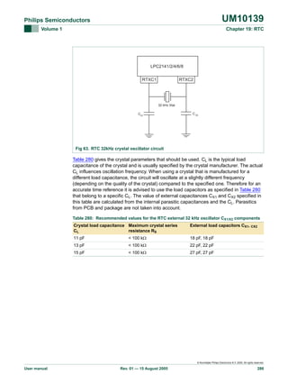
![UM10139
Philips Semiconductors
Volume 1
Chapter 20: WDT
20.4 Register description
The watchdog contains 4 registers as shown in Table 281 below.
Table 281: Watchdog register map
Name
Description
Access Reset
Address
value[1]
WDMOD
Watchdog Mode register. This register contains
R/W
the basic mode and status of the Watchdog Timer.
0
0xE000 0000
WDTC
Watchdog Timer Constant register. This register
determines the time-out value.
R/W
0xFF
0xE000 0004
WO
NA
0xE000 0008
0xFF
0xE000 000C
WDFEED Watchdog Feed sequence register. Writing 0xAA
followed by 0x55 to this register reloads the
Watchdog timer to its preset value.
WDTV
[1]
Watchdog Timer Value register. This register reads RO
out the current value of the Watchdog timer.
Reset value reflects the data stored in used bits only. It does not include reserved bits content.
20.4.1 Watchdog Mode register (WDMOD - 0xE000 0000)
The WDMOD register controls the operation of the watchdog as per the combination of
WDEN and RESET bits.
Table 282: Watchdog operating modes selection
WDEN
WDRESET
Mode of Operation
0
X (0 or 1)
Debug/Operate without the watchdog running.
1
0
Watchdog Interrupt Mode: debug with the Watchdog interrupt but no
WDRESET enabled.
When this mode is selected, a watchdog counter underflow will set the
WDINT flag and the watchdog interrupt request will be generated.
1
1
Watchdog Reset Mode: operate with the watchdog interrupt and
WDRESET enabled.
When this mode is selected, a watchdog counter underflow will reset
the microcontroller. While the watchdog interrupt is also enabled in
this case (WDEN = 1) it will not be recognized since the watchdog
reset will clear the WDINT flag.
Once the WDEN and/or WDRESET bits are set they can not be cleared by software. Both
flags are cleared by an external reset or a watchdog timer underflow.
WDTOF The Watchdog Time-Out Flag is set when the watchdog times out. This flag is
cleared by software.
WDINT The Watchdog Interrupt Flag is set when the watchdog times out. This flag is
cleared when any reset occurs. Once the watchdog interrupt is serviced, it can be
disabled in the VIC or the watchdog interrupt request will be generated indefinitely.
© Koninklijke Philips Electronics N.V. 2005. All rights reserved.
User manual
Rev. 01 — 15 August 2005
288](https://image.slidesharecdn.com/armusrmanl-131212220701-phpapp02/85/Arm-usr-m-anl-288-320.jpg)
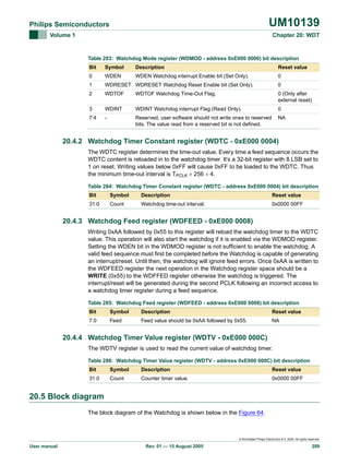
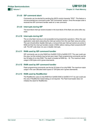
![UM10139
Philips Semiconductors
Volume 1
Chapter 21: Flash Memory
boot block is present at addresses 0x0007 D000 to 0x0007 FFFF in all devices. ISP and
IAP commands do not allow write/erase/go operation on the boot block. Because of the
boot block, the amount of Flash available for user code and data is 500 K bytes in "512K"
devices. On the other hand, in case of the LPC2141/2/4/6 microcontroller all
32/64/128/256 K of Flash are available for user’s application.
Sector
Number
Sector
Size [kB]
Address Range
LPC2141
(32kB)
LPC2142
(64kB)
LPC2144
(128kB)
LPC2146
(256kB)
LPC2148
(512kB)
Table 287: Flash sectors in LPC2141, LPC2142, LPC2144, LPC2146 and LPC2148
0
4
0X0000 0000 - 0X0000 0FFF
+
+
+
+
+
1
4
0X0000 1000 - 0X0000 1FFF
+
+
+
+
+
2
4
0X0000 2000 - 0X0000 2FFF
+
+
+
+
+
3
4
0X0000 3000 - 0X0000 3FFF
+
+
+
+
+
4
4
0X0000 4000 - 0X0000 4FFF
+
+
+
+
+
5
4
0X0000 5000 - 0X0000 5FFF
+
+
+
+
+
6
4
0X0000 6000 - 0X0000 6FFF
+
+
+
+
+
7
4
0X0000 7000 - 0X0000 7FFF
+
+
+
+
+
8
32
0x0000 8000 - 0X0000 FFFF
+
+
+
+
9
32
0x0001 0000 - 0X0001 7FFF
+
+
+
10 (0x0A)
32
0x0001 8000 - 0X0001 FFFF
+
+
+
11 (0x0B)
32
0x0002 0000 - 0X0002 7FFF
+
+
12 (0x0C)
32
0x0002 8000 - 0X0002 FFFF
+
+
13 (0x0D)
32
0x0003 0000 - 0X0003 7FFF
+
+
14 (0X0E)
32
0x0003 8000 - 0X0003 FFFF
+
+
15 (0x0F)
32
0x0004 0000 - 0X0004 7FFF
+
16 (0x10)
32
0x0004 8000 - 0X0004 FFFF
+
17 (0x11)
32
0x0005 0000 - 0X0005 7FFF
+
18 (0x12)
32
0x0005 8000 - 0X0005 FFFF
+
19 (0x13)
32
0x0006 0000 - 0X0006 7FFF
+
20 (0x14)
32
0x0006 8000 - 0X0006 FFFF
+
21 (0x15)
32
0x0007 0000 - 0X0007 7FFF
+
22 (0x16)
4
0x0007 8000 - 0X0007 8FFF
+
23 (0x17)
4
0x0007 9000 - 0X0007 9FFF
+
24 (0x18)
4
0x0007 A000 - 0X0007 AFFF
+
25 (0x19)
4
0x0007 B000 - 0X0007 BFFF
+
26 (0x1A)
4
0x0007 C000 - 0X0007 CFFF
+
21.6 Flash content protection mechanism
The LPC2141/2/4/6/8 is equipped with the Error Correction Code (ECC) capable Flash
memory. The purpose of an error correction module is twofold. Firstly, it decodes data
words read from the memory into output data words. Secondly, it encodes data words to
be written to the memory. The error correction capability consists of single bit error
correction with Hamming code.
© Koninklijke Philips Electronics N.V. 2005. All rights reserved.
User manual
Rev. 01 — 15 August 2005
296](https://image.slidesharecdn.com/armusrmanl-131212220701-phpapp02/85/Arm-usr-m-anl-296-320.jpg)
![UM10139
Philips Semiconductors
Volume 1
Chapter 21: Flash Memory
Table 304: ISP Return codes Summary
Return Mnemonic
Code
Description
12
PARAM_ERROR
Insufficient number of parameters or invalid
parameter.
13
ADDR_ERROR
Address is not on word boundary.
14
ADDR_NOT_MAPPED
Address is not mapped in the memory map. Count
value is taken in to consideration where applicable.
15
CMD_LOCKED
Command is locked.
16
INVALID_CODE
Unlock code is invalid.
17
INVALID_BAUD_RATE
Invalid baud rate setting.
18
INVALID_STOP_BIT
Invalid stop bit setting.
19
CODE_READ_PROTECTION_
ENABLED
Code read protection enabled.
21.9 IAP Commands
For in application programming the IAP routine should be called with a word pointer in
register r0 pointing to memory (RAM) containing command code and parameters. Result
of the IAP command is returned in the result table pointed to by register r1. The user can
reuse the command table for result by passing the same pointer in registers r0 and r1. The
parameter table should be big enough to hold all the results in case if number of results
are more than number of parameters. Parameter passing is illustrated in the Figure 67.
The number of parameters and results vary according to the IAP command. The
maximum number of parameters is 5, passed to the "Copy RAM to FLASH" command.
The maximum number of results is 2, returned by the "Blankcheck sector(s)" command.
The command handler sends the status code INVALID_COMMAND when an undefined
command is received. The IAP routine resides at 0x7FFF FFF0 location and it is thumb
code.
The IAP function could be called in the following way using C.
Define the IAP location entry point. Since the 0th bit of the IAP location is set there will be
a change to Thumb instruction set when the program counter branches to this address.
#define IAP_LOCATION 0x7ffffff1
Define data structure or pointers to pass IAP command table and result table to the IAP
function:
unsigned long command[5];
unsigned long result[2];
or
unsigned long * command;
unsigned long * result;
command=(unsigned long *) 0x……
result= (unsigned long *) 0x……
Define pointer to function type, which takes two parameters and returns void. Note the IAP
returns the result with the base address of the table residing in R1.
© Koninklijke Philips Electronics N.V. 2005. All rights reserved.
User manual
Rev. 01 — 15 August 2005
305](https://image.slidesharecdn.com/armusrmanl-131212220701-phpapp02/85/Arm-usr-m-anl-305-320.jpg)
![UM10139
Philips Semiconductors
Volume 1
Chapter 21: Flash Memory
typedef void (*IAP)(unsigned int [],unsigned int[]);
IAP iap_entry;
Setting function pointer:
iap_entry=(IAP) IAP_LOCATION;
Whenever you wish to call IAP you could use the following statement.
iap_entry (command, result);
The IAP call could be simplified further by using the symbol definition file feature
supported by ARM Linker in ADS (ARM Developer Suite). You could also call the IAP
routine using assembly code.
The following symbol definitions can be used to link IAP routine and user application:
#<SYMDEFS># ARM Linker, ADS1.2 [Build 826]: Last Updated: Wed May 08 16:12:23 2002
0x7fffff90 T rm_init_entry
0x7fffffa0 A rm_undef_handler
0x7fffffb0 A rm_prefetchabort_handler
0x7fffffc0 A rm_dataabort_handler
0x7fffffd0 A rm_irqhandler
0x7fffffe0 A rm_irqhandler2
0x7ffffff0 T iap_entry
As per the ARM specification (The ARM Thumb Procedure Call Standard SWS ESPC
0002 A-05) up to 4 parameters can be passed in the r0, r1, r2 and r3 registers
respectively. Additional parameters are passed on the stack. Up to 4 parameters can be
returned in the r0, r1, r2 and r3 registers respectively. Additional parameters are returned
indirectly via memory. Some of the IAP calls require more than 4 parameters. If the ARM
suggested scheme is used for the parameter passing/returning then it might create
problems due to difference in the C compiler implementation from different vendors. The
suggested parameter passing scheme reduces such risk.
The flash memory is not accessible during a write or erase operation. IAP commands,
which results in a flash write/erase operation, use 32 bytes of space in the top portion of
the on-chip RAM for execution. The user program should not be use this space if IAP flash
programming is permitted in the application.
Table 305: IAP Command Summary
IAP Command
Command Code
Described in
Prepare sector(s) for write operation
5010
Table 306
Copy RAM to Flash
5110
Table 307
Erase sector(s)
5210
Table 308
Blank check sector(s)
5310
Table 309
Read Part ID
5410
Table 310
Read Boot code version
5510
Table 311
Compare
5610
Table 312
Reinvoke ISP
5710
Table 313
© Koninklijke Philips Electronics N.V. 2005. All rights reserved.
User manual
Rev. 01 — 15 August 2005
306](https://image.slidesharecdn.com/armusrmanl-131212220701-phpapp02/85/Arm-usr-m-anl-306-320.jpg)
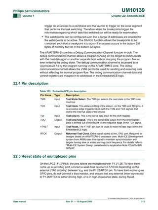
![UM10139
Chapter 23: Embedded Trace Macrocell (ETM)
Rev. 01 — 15 August 2005
User manual
23.1 Features
•
•
•
•
•
•
Closely track the instructions that the ARM core is executing.
1 External trigger input
10 pin interface
All registers are programmed through JTAG interface.
Does not consume power when trace is not being used.
THUMB instruction set support
23.2 Applications
As the microcontroller has significant amounts of on-chip memories, it is not possible to
determine how the processor core is operating simply by observing the external pins. The
ETM provides real-time trace capability for deeply embedded processor cores. It outputs
information about processor execution to a trace port. A software debugger allows
configuration of the ETM using a JTAG interface and displays the trace information that
has been captured, in a format that a user can easily understand.
23.3 Description
The ETM is connected directly to the ARM core and not to the main AMBA system bus. It
compresses the trace information and exports it through a narrow trace port. An external
Trace Port Analyzer captures the trace information under software debugger control. Trace
port can broadcast the Instruction trace information. Instruction trace (or PC trace) shows
the flow of execution of the processor and provides a list of all the instructions that were
executed. Instruction trace is significantly compressed by only broadcasting branch
addresses as well as a set of status signals that indicate the pipeline status on a cycle by
cycle basis. Trace information generation can be controlled by selecting the trigger
resource. Trigger resources include address comparators, counters and sequencers.
Since trace information is compressed the software debugger requires a static image of
the code being executed. Self-modifying code can not be traced because of this
restriction.
23.3.1 ETM configuration
The following standard configuration is selected for the ETM macrocell.
Table 317: ETM configuration
Resource number/type
Small[1]
Pairs of address comparators
1
Data Comparators
0 (Data tracing is not supported)
Memory Map Decoders
4
Counters
1
Sequencer Present
No
© Koninklijke Philips Electronics N.V. 2005. All rights reserved.
User manual
Rev. 01 — 15 August 2005
315](https://image.slidesharecdn.com/armusrmanl-131212220701-phpapp02/85/Arm-usr-m-anl-315-320.jpg)
![UM10139
Philips Semiconductors
Volume 1
Chapter 23: Embedded Trace
Table 317: ETM configuration
Resource number/type
Small[1]
External Inputs
2
External Outputs
0
FIFOFULL Present
Yes (Not wired)
FIFO depth
10 bytes
Trace Packet Width
4/8
[1]
For details refer to ARM documentation "Embedded Trace Macrocell Specification (ARM IHI 0014E)".
23.4 Pin description
Table 318: ETM pin description
Pin Name
Type
Description
TRACECLK
Output Trace Clock. The trace clock signal provides the clock for the trace
port. PIPESTAT[2:0], TRACESYNC, and TRACEPKT[3:0] signals are
referenced to the rising edge of the trace clock. This clock is not
generated by the ETM block. It is to be derived from the system clock.
The clock should be balanced to provide sufficient hold time for the
trace data signals. Half rate clocking mode is supported. Trace data
signals should be shifted by a clock phase from TRACECLK. Refer to
Figure 3.14 page 3.26 and figure 3.15 page 3.27 in "ETM7 Technical
Reference Manual" (ARM DDI 0158B), for example circuits that
implements both half-rate clocking and shifting of the trace data with
respect to the clock. For TRACECLK timings refer to section 5.2 on
page 5-13 in "Embedded Trace Macrocell Specification" (ARM IHI
0014E).
PIPESTAT[2:0]
Output Pipe Line status. The pipeline status signals provide a cycle-by-cycle
indication of what is happening in the execution stage of the processor
pipeline.
TRACESYNC
Output Trace synchronization. The trace sync signal is used to indicate the
first packet of a group of trace packets and is asserted HIGH only for
the first packet of any branch address.
TRACEPKT[3:0] Output Trace Packet. The trace packet signals are used to output packaged
address and data information related to the pipeline status. All packets
are eight bits in length. A packet is output over two cycles. In the first
cycle, Packet[3:0] is output and in the second cycle, Packet[7:4] is
output.
EXTIN[0]
Input
External Trigger Input
23.5 Reset state of multiplexed pins
On the LPC2141/2/4/6/8, the ETM pin functions are multiplexed with P1.25-16. To have
these pins come as a Trace port, connect a weak bias resistor (4.7 kΩ) between the
P1.20/TRACESYNC pin and VSS. To have them come up as port pins, do not connect a
bias resistor to P1.20/TRACESYNC, and ensure that any external driver connected to
P1.20/TRACESYNC is either driving high, or is in high-impedance state, during Reset.
© Koninklijke Philips Electronics N.V. 2005. All rights reserved.
User manual
Rev. 01 — 15 August 2005
316](https://image.slidesharecdn.com/armusrmanl-131212220701-phpapp02/85/Arm-usr-m-anl-316-320.jpg)
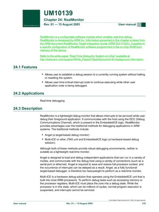
![UM10139
Philips Semiconductors
Volume 1
Chapter 24: RealMonitor
LDR pc, [pc, #-0xFF0] ;Load IRQ vector from VIC
LDR PC, FIQ_Address
Reset_Address
Undefined_Address
SWI_Address
Prefetch_Address
Abort_Address
FIQ_Address
DCD
DCD
DCD
DCD
DCD
DCD
__init
;Reset Entry point
rm_undef_handler ;Provided by RealMonitor
0
;User can put address of SWI handler here
rm_prefetchabort_handler
;Provided by RealMonitor
rm_dataabort_handler
;Provided by RealMonitor
0
;User can put address of FIQ handler here
AREA init_code, CODE
ram_end EQU 0x4000xxxx ; Top of on-chip RAM.
__init
; /*********************************************************************
; * Set up the stack pointers for various processor modes. Stack grows
; * downwards.
; *********************************************************************/
LDR r2, =ram_end ;Get top of RAM
MRS r0, CPSR ;Save current processor mode
; Initialize the Undef mode stack for RealMonitor use
BIC r1, r0, #0x1f
ORR r1, r1, #0x1b
MSR CPSR_c, r1
;Keep top 32 bytes for flash programming routines.
;Refer to Flash Memory System and Programming chapter
SUB sp,r2,#0x1F
; Initialize the Abort mode stack for RealMonitor
BIC r1, r0, #0x1f
ORR r1, r1, #0x17
MSR CPSR_c, r1
;Keep 64 bytes for Undef mode stack
SUB sp,r2,#0x5F
; Initialize the IRQ mode stack for RealMonitor and User
BIC r1, r0, #0x1f
ORR r1, r1, #0x12
MSR CPSR_c, r1
;Keep 32 bytes for Abort mode stack
SUB sp,r2,#0x7F
; Return to the original mode.
MSR CPSR_c, r0
; Initialize the stack for user application
; Keep 256 bytes for IRQ mode stack
SUB sp,r2,#0x17F
; /*********************************************************************
© Koninklijke Philips Electronics N.V. 2005. All rights reserved.
User manual
Rev. 01 — 15 August 2005
325](https://image.slidesharecdn.com/armusrmanl-131212220701-phpapp02/85/Arm-usr-m-anl-325-320.jpg)
![UM10139
Philips Semiconductors
Volume 1
Chapter 24: RealMonitor
;
;
;
;
;
;
;
* Setup Vectored Interrupt controller. DCC Rx and Tx interrupts
* generate Non Vectored IRQ request. rm_init_entry is aware
* of the VIC and it enables the DBGCommRX and DBGCommTx interrupts.
* Default vector address register is programmed with the address of
* Non vectored app_irqDispatch mentioned in this example. User can setup
* Vectored IRQs or FIQs here.
*********************************************************************/
VICBaseAddr
EQU 0xFFFFF000 ; VIC Base address
VICDefVectAddrOffset EQU 0x34
LDR
LDR
STR
r0, =VICBaseAddr
r1, =app_irqDispatch
r1, [r0,#VICDefVectAddrOffset]
BL
rm_init_entry
;Initialize RealMonitor
;enable FIQ and IRQ in ARM Processor
MRS r1, CPSR
; get the CPSR
BIC r1, r1, #0xC0
; enable IRQs and FIQs
MSR CPSR_c, r1
; update the CPSR
; /*********************************************************************
; * Get the address of the User entry point.
; *********************************************************************/
LDR lr, =User_Entry
MOV pc, lr
; /*********************************************************************
; * Non vectored irq handler (app_irqDispatch)
; *********************************************************************/
AREA app_irqDispatch, CODE
VICVectAddrOffset EQU 0x30
app_irqDispatch
;enable interrupt nesting
STMFD sp!, {r12,r14}
MRS r12, spsr
MSR cpsr_c,0x1F
;Save SPSR in to r12
;Re-enable IRQ, go to system mode
;User should insert code here if non vectored Interrupt sharing is
;required. Each non vectored shared irq handler must return to
;the interrupted instruction by using the following code.
;
MSR cpsr_c, #0x52
;Disable irq, move to IRQ mode
;
MSR spsr, r12
;Restore SPSR from r12
;
STMFD sp!, {r0}
;
LDR r0, =VICBaseAddr
;
STR r1, [r0,#VICVectAddrOffset]
;Acknowledge Non Vectored irq has finished
;
LDMFD sp!, {r12,r14,r0}
;Restore registers
;
SUBS pc, r14, #4
;Return to the interrupted instruction
;user interrupt did not happen so call rm_irqhandler2. This handler
;is not aware of the VIC interrupt priority hardware so trick
;rm_irqhandler2 to return here
© Koninklijke Philips Electronics N.V. 2005. All rights reserved.
User manual
Rev. 01 — 15 August 2005
326](https://image.slidesharecdn.com/armusrmanl-131212220701-phpapp02/85/Arm-usr-m-anl-326-320.jpg)
![UM10139
Philips Semiconductors
Volume 1
Chapter 24: RealMonitor
STMFD sp!, {ip,pc}
LDR pc, rm_irqhandler2
;rm_irqhandler2 returns here
MSR cpsr_c, #0x52
MSR spsr, r12
STMFD sp!, {r0}
LDR r0, =VICBaseAddr
STR r1, [r0,#VICVectAddrOffset]
LDMFD sp!, {r12,r14,r0}
SUBS pc, r14, #4
END
;Disable irq, move to IRQ mode
;Restore SPSR from r12
;Acknowledge Non Vectored irq has finished
;Restore registers
;Return to the interrupted instruction
24.5 RealMonitor build options
RealMonitor was built with the following options:
RM_OPT_DATALOGGING=FALSE
This option enables or disables support for any target-to-host packets sent on a non
RealMonitor (third-party) channel.
RM_OPT_STOPSTART=TRUE
This option enables or disables support for all stop and start debugging features.
RM_OPT_SOFTBREAKPOINT=TRUE
This option enables or disables support for software breakpoints.
RM_OPT_HARDBREAKPOINT=TRUE
Enabled for cores with EmbeddedICE-RT. This device uses ARM-7TDMI-S Rev 4 with
EmbeddedICE-RT.
RM_OPT_HARDWATCHPOINT=TRUE
Enabled for cores with EmbeddedICE-RT. This device uses ARM-7TDMI-S Rev 4 with
EmbeddedICE-RT.
RM_OPT_SEMIHOSTING=FALSE
This option enables or disables support for SWI semi-hosting. Semi-hosting provides
code running on an ARM target use of facilities on a host computer that is running an
ARM debugger. Examples of such facilities include the keyboard input, screen output,
and disk I/O.
RM_OPT_SAVE_FIQ_REGISTERS=TRUE
This option determines whether the FIQ-mode registers are saved into the registers
block when RealMonitor stops.
RM_OPT_READBYTES=TRUE
RM_OPT_WRITEBYTES=TRUE
RM_OPT_READHALFWORDS=TRUE
© Koninklijke Philips Electronics N.V. 2005. All rights reserved.
User manual
Rev. 01 — 15 August 2005
327](https://image.slidesharecdn.com/armusrmanl-131212220701-phpapp02/85/Arm-usr-m-anl-327-320.jpg)
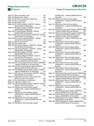
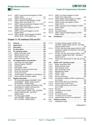


![Pic microcontroller [autosaved] [autosaved]](https://cdn.slidesharecdn.com/ss_thumbnails/picmicrocontrollerautosavedautosaved-120427093459-phpapp02-thumbnail.jpg?width=640&height=640&fit=bounds)