Fundamentals of Electronics Engineering (FEE) serves as the cornerstone for students pursuing studies in electronics, electrical, communication, instrumentation, and computer-related engineering disciplines. It provides the essential theoretical and practical knowledge required to understand, design, and analyze electronic systems and devices that form the basis of modern technology.
At its core, FEE covers a broad spectrum of topics that include basic electrical concepts, semiconductor physics, analog circuits, digital electronics, and electronic communication principles. The journey begins with understanding electrical quantities such as voltage, current, resistance, power, and energy, and how these are governed by foundational laws like Ohm’s Law, Kirchhoff’s Voltage and Current Laws, and network theorems such as Thevenin’s, Norton’s, and Superposition theorems.
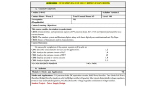
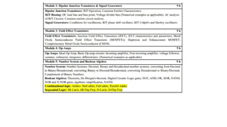
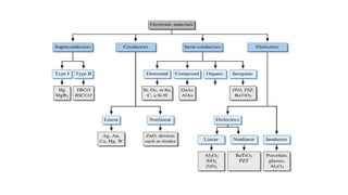
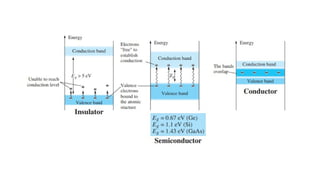
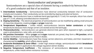
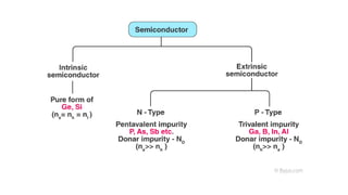
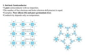
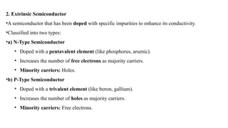
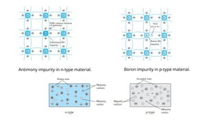
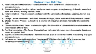
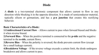
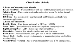
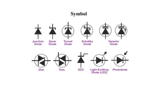
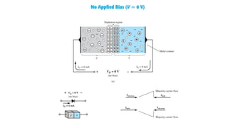
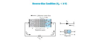
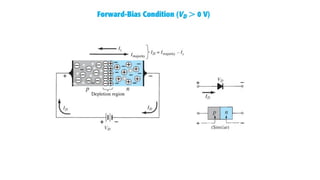
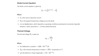
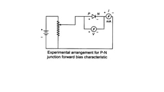
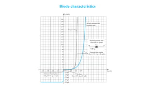
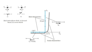
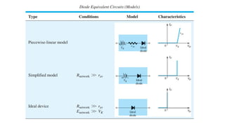
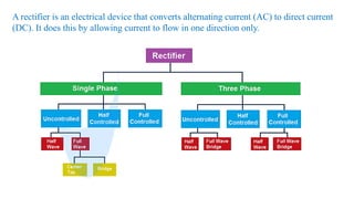
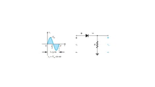
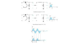
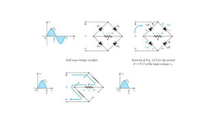
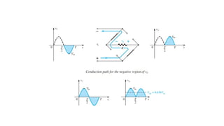
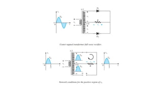
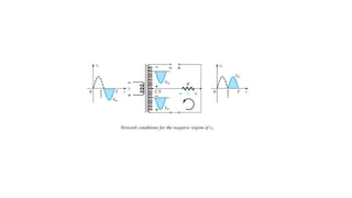
An integral part of electronics is the behavior of semiconductor materials, primarily silicon and germanium, which are the building blocks of diodes, transistors, and integrated circuits. Students are introduced to the operation of p-n junction diodes, Zener diodes, and light-emitting diodes (LEDs), along with their applications in rectifiers, voltage regulators, and signal modulation.
The study of bipolar junction transistors (BJTs) and field-effect transistors (FETs) follows, where emphasis is placed on their configurations, input/output characteristics, and use in amplifier and switch circuits. This forms the basis for understanding analog electronics, including single-stage and multi-stage amplifiers, feedback systems, and oscillator circuits like RC and LC oscillators.
Parallel to analog systems, digital electronics introduces the binary number system, Boolean algebra, logic gates, combinational and sequential circuits, flip-flops, counters, and memory systems. These concepts are essential for understanding how modern computers and embedded systems function.
Furthermore, FEE encompasses the basics of electronic instrumentation and measurement, including the principles behind oscilloscopes, multimeters, signal generators, and other diagnostic tools used in electronic laboratories.
An introductory overview of communication systems is also part of the curriculum. It typically includes the classification of signals, the need for modulation, and a brief explanation of AM, FM, and digital communication techniques. These concepts lay the foundation for more advanced studies in wireless systems, mobile communication, and IoT (Internet of Things).
The course not only emphasizes theoretical understanding but also encourages hands-on learning through lab sessions, circuit design projects, and simulation software such as Multisim or Proteus. This approach equips students with the confidence and competence to troubleshoot and build basic electronic systems.
In summary, Fundamentals of Electronics Engineering is a multidisciplinary gateway that nurtures logical thinking, problem-solving