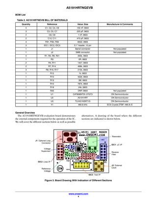
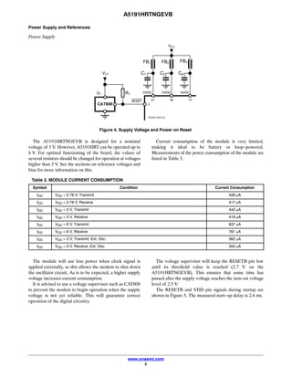
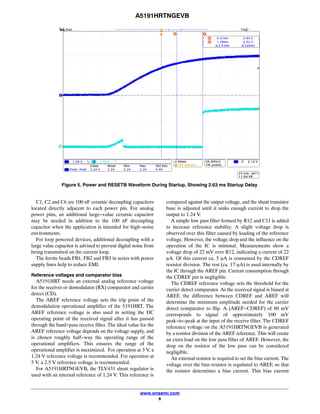
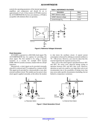
Download to read offline
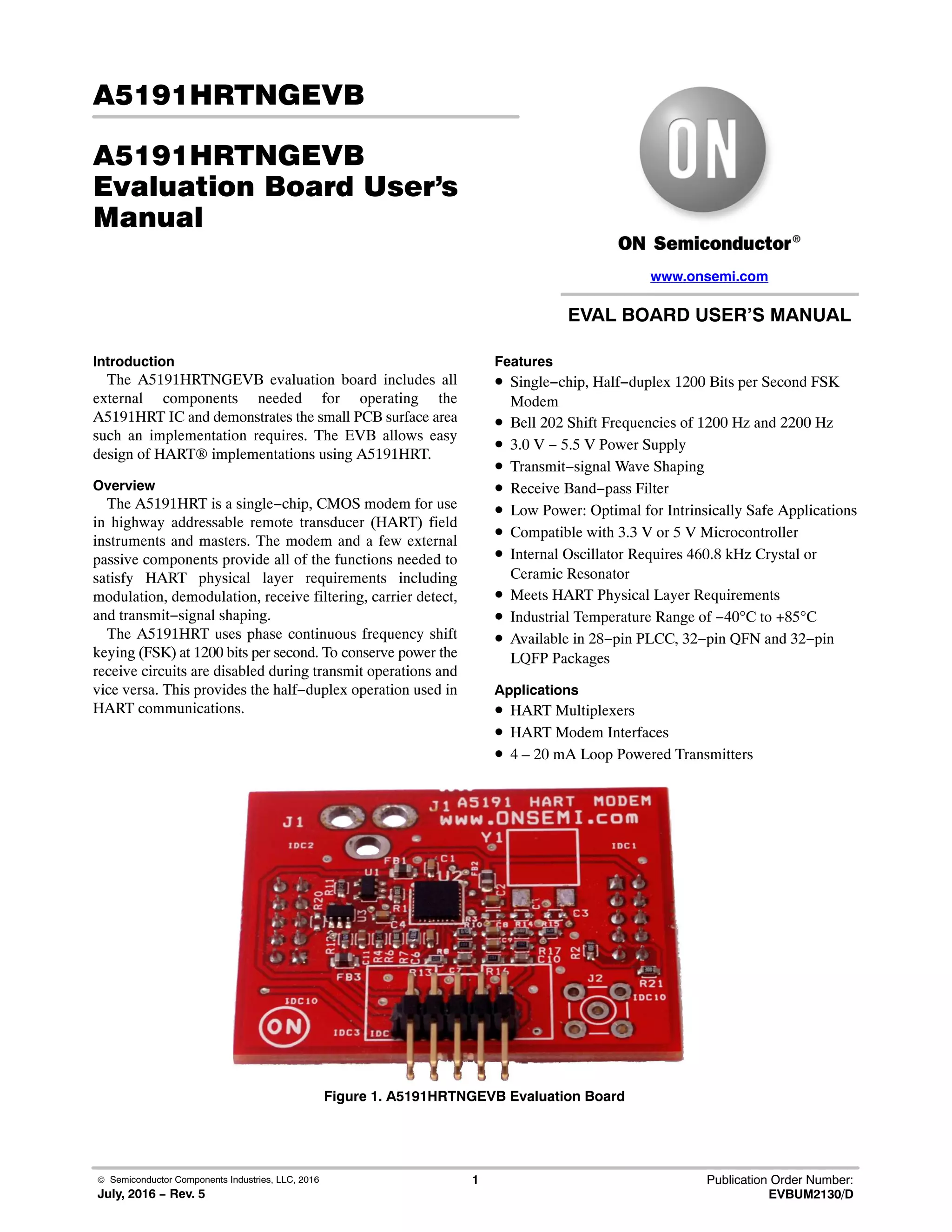

This document provides an overview and evaluation of the A5191HRTNGEVB evaluation board, which demonstrates the external components needed for operating the A5191HRT IC for HART communications. The board allows testing the IC's small PCB footprint and easy design of HART implementations. Key sections described include the power supply, reference voltages, clock generation, and schematic. Electrical characteristics and a bill of materials are also provided.


