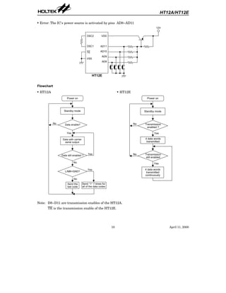
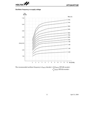
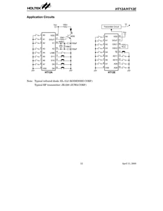
The document describes two CMOS LSIs, the HT12A and HT12E, which are encoders for remote control systems. They can encode information consisting of N address bits and 12-N data bits. The HT12A provides a 38kHz carrier for infrared transmission and allows selection of a data trigger, while the HT12E allows selection of a TE trigger. Upon receiving a trigger signal, the encoded addresses and data are transmitted in a series of words. The encoders can operate from 2.4-5V for the HT12A and 2.4-12V for the HT12E, with low power consumption.
Electrónica: HT12D + HT12E / Codificador y decodificador serial de datos para...SANTIAGO PABLO ALBERTO
The document describes the 212 series of decoders from Holtek. It provides three key details:
1) The 212 series of decoders can decode up to 12 bits of address and data information from encoded signals transmitted by 212 series encoders. They include models with different combinations of address and data pins.
2) The decoders receive serial data from an encoder, compare the address to an internal address, and output the data if the addresses match. They check the address three times to ensure valid transmission.
3) Applications include security systems, remote controls, and other devices using radio or infrared transmission of encoded signals between encoders and decoders.
The document describes the HT12D and HT12F decoders. The decoders receive serial addresses and data from encoders and decode the information. The HT12D provides 8 address bits and 4 data bits as outputs, while the HT12F decodes 12 address bits and provides a momentary valid transmission indicator. The decoders operate between 2.4-12V and require a resistor connected oscillator to function properly paired with Holtek encoders.
Cell Phone Controlled Home Automation System using DTMF TechnologyTaufique Sekh
This home appliances control or home automation project uses DTMF decoder circuit to control home and office electrical appliances. Just connect your cell phone headset (headphone) jack to the mobile phone and then mobile will control electrical appliances and electrical equipment through the DTMF key pad of your cell phone. Here for demonstrating, we are controlling an electrical bulb using this circuit project but you can extend this circuit to control many electrical devices with some modifications using4×16 decoder IC.
Electrónica: Receptor DTMF integrado MT8870D/MT8870D-1 (Datasheet)SANTIAGO PABLO ALBERTO
The MT8870D/MT8870D-1 is a complete DTMF receiver integrated circuit that detects DTMF tones. It has a filter section that separates high and low group tones and a digital decoder that detects and decodes the 16 DTMF tone pairs into a 4-bit output code. It has low power consumption and integrates the bandsplit filter and digital decoder functions onto a single chip. The chip can be configured to meet various system requirements by adjusting the external steering time constants to select the guard times for tone detection and interdigital pauses.
The document discusses the 8086/8088 microprocessors. It describes their basic features, including being 16-bit microprocessors introduced in 1978/1979 and using HMOS technology. It also covers their pin configurations and diagrams, addressing modes, minimum and maximum modes, and descriptions of the various pins and signals.
This document provides specifications and installation instructions for the HE-XE102-10 module. It includes:
- Specifications for the module's 12 digital inputs, 2 analog inputs, 6 relay outputs, and 2 thermistor inputs.
- Instructions for panel cut-out, ports/connectors, wiring, jumper settings, and derating relay life expectancy.
- Details on the module's digital and analog filtering, thermistor linearization, and recommended filter constant setting.
The TDA5051A is a modem IC designed for ASK data transmission over home power lines at 600 or 1200 baud. It features fully digital carrier generation and modulation/demodulation, with an integrated output power stage. The IC requires few external components and operates from a single 5V supply. It is intended for applications such as home automation, energy control, and transmitting data over power lines using amplitude shift keying modulation at carrier frequencies up to 132.5 kHz.
This document describes the DM74LS74A dual positive-edge triggered D flip-flop integrated circuit. It contains two independent D flip-flops that sample data on the positive edge of the clock signal. Each flip-flop has preset and clear inputs to force the outputs, and complementary Q and Q-bar outputs. The document provides pinout diagrams, truth tables, electrical specifications, and packaging/dimension information.
This document describes a remote home appliance control project. It includes the objective to help elderly or disabled people control appliances remotely. The block diagram shows the transmitter uses an HT12E encoder, 555 timer, AND gate and IR LED to transmit switch states via infrared signals. The receiver uses an IR receiver, HT12D decoder, ULN2003 relay driver and relays to control loads based on the received signals. Circuit diagrams and component explanations are provided for the transmitter and receiver. The project also includes a PCB layout and photos of the completed project.
This document describes the DM74LS74A dual positive-edge triggered D flip-flop integrated circuit. It contains two independent D flip-flops that accept input on the positive edge of the clock signal. Each flip-flop has preset and clear inputs to force the outputs, and complementary Q and Q-bar outputs. The document provides pinout diagrams, truth tables, electrical specifications, and packaging/dimension information.
Bluetooth based home appliances controlPROJECTRONICS
This document describes a Bluetooth-based home appliance control system that allows appliances to be operated remotely using a Bluetooth-enabled device like a smartphone. The system uses a microcontroller interfaced with a Bluetooth module to receive commands from a mobile app and control electrical loads accordingly. It consists of a power supply, DTMF decoder to receive signals from Bluetooth, motor driver, solid state relays, and other circuits. The system was designed and tested successfully in the lab to allow remote control of appliances in a way that helps elderly or disabled people. Potential future expansions are also discussed.
This document provides information about a wireless serial communication RF modem module that operates at 2.4 GHz with a range of 30 meters. It can transmit and receive data at multiple baud rates and supports half-duplex communication. The module has features such as multiple channel selection, operation in the unlicensed 2.4 GHz band, and a standard UART interface. Example applications and specifications are also provided, along with code samples for interfacing the module with an 8051 microcontroller and a PC.
This document provides information about a wireless serial communication RF modem module that operates at 2.4 GHz with a range of 30 meters. It can transmit and receive data at multiple baud rates and supports half-duplex communication. The module has features such as multiple channel selection, compatibility with the unlicensed 2.4 GHz ISM band, and plug-and-play operation. Specifications, pinouts, operating instructions, and code examples for interfacing the module with an 8051 microcontroller and PC are also included.
This document provides an instruction sheet for the DVP28SV PLC. It summarizes the PLC's specifications including its size, inputs/outputs, memory capacity, instructions, and electrical specifications. It also provides information on installing the PLC properly and warnings about connecting power. Diagrams show the front panel layout and outline dimensions. Tables further describe the PLC's features such as I/O types, timers, counters, relays, and more.
The document describes the analog-to-digital converter (A/D) module for PIC18F2455/2550/4455/4550 microcontrollers. The module allows conversion of an analog input signal to a 10-bit digital number. It has 10 or 13 analog input channels depending on the device, and is controlled using three registers - ADCON0, ADCON1, and ADCON2. The ADRESH and ADRESL registers together contain the 10-bit digital output of the A/D conversion.
The document discusses the architecture, programming, and interfacing of microprocessors using the 8086 as an example. It describes two models used to study microprocessors: the programmer's model which shows internal registers and buses, and the hardware model which shows pin diagrams. It then discusses the basic components of a microcomputer system using an 8086, including memory, I/O devices, and different types of buses. Finally, it provides details on the 8086 architecture, registers, addressing modes, and timing sequences for read and write cycles.
The document provides an introduction to PDH and SDH technologies, describing the frame structures and multiplexing hierarchies of PDH and how SDH was developed as an international standard to address limitations of PDH such as lack of world standards for digital formats and optical interfaces. Key aspects of SDH are explained including the STM frame structure, multiplexing structure, path layers, pointer processing, and overhead bytes.
The P89V51RD2 is an 80C51 microcontroller with 64kB of Flash memory and 1kB of RAM. It has features like In-System Programming, In-Application Programming, and a choice of running at the standard 80C51 clock rate or twice the throughput at the same clock frequency in X2 mode. It includes ports, timers, serial interfaces, and low power modes.
The document describes the features and specifications of the DSP56824 16-bit digital signal processor, including its programmable peripherals, memory capabilities, and interface options. It is well-suited for cost-sensitive applications like digital wireless devices and cameras due to its low cost, configuration flexibility, and compact code. The evaluation module provides peripherals like memory, a codec, LEDs, and buttons to help develop and test applications for the DSP56824.
The document discusses various peripherals on microcontrollers including parallel I/O ports (P0-3), timers/counters, DAC, ADC, PWM, UART. It provides details on how each peripheral works, the registers used to control them, and examples of using timers/counters and DAC to generate waveforms.
The document discusses various peripherals that can be used on microcontrollers for communicating with external devices. It describes peripherals such as parallel and serial input/output ports, analog-to-digital converters, digital-to-analog converters, pulse-width modulators, timers/counters, and universal asynchronous receiver/transmitters. Specific registers and parameters for configuring and controlling these peripherals on a microcontroller are also outlined.
This document describes an RF ID based access control system. The system uses an RF transmitter kit that sends an RF ID to a receiver circuit. If the received ID matches the data in the receiver, the name of the RF ID holder is displayed on an LCD. The project is divided into three parts: 1) RF ID code transmission using an RF ID encoder IC, 2) Receiving the RF ID data using the main receiver, 3) Opening the door if the password matches. A master can also open the door with a password.
Upon completion of this course, students will learn about the functions, hardware structure, and cable connections of BTS (Base Transceiver Station). The document provides an overview of BTS system components and signal processing. It also describes the typical BTS configuration and introduces the main hardware components of the BTS3012 cabinet, including their functions.
An embedded system is closely integrated with the main system
It may not interact directly with the environment
For example – A microcomputer in a car ignition control
The LT9611UXC is a dual-port MIPI DSI/CSI to HDMI 2.0 converter with audio support. It features a single or dual-port MIPI receiver and HDMI 2.0 transmitter that can support video formats up to 4K at 60Hz. It also supports various audio input formats at sample rates up to 192kHz. The device integrates functions including color space conversion, an embedded processor, and firmware storage to enable automatic operation. It is intended for applications such as set-top boxes and DVD players.
The LM3914 is an integrated circuit that senses analog voltage levels and drives 10 LEDs to provide a linear analog display. It contains an adjustable voltage reference and accurate 10-step voltage divider to compare input voltages. The outputs are individually current regulated and can drive LEDs, LCDs, or vacuum fluorescent displays in either a moving dot or bar graph display mode. The simple circuit requires few external components and can operate over a wide supply voltage range from less than 3V.
The document provides information about the LM386 low voltage audio power amplifier, including:
1) It describes the key features, applications, and functional description of the LM386 amplifier.
2) It provides the typical application schematic showing the minimum external components needed to use the LM386 with its internally set gain of 20.
3) It discusses designing the LM386 amplifier circuit, including controlling the gain from 20 to 200 by adding external resistors and capacitors between pins 1 and 8.
The LM380 is a 2.5W audio power amplifier integrated circuit suitable for consumer applications. It has a fixed gain of 34dB, operates from a 10-22V supply, and features high peak current capability, input referenced to ground, and short circuit protection. Typical uses include phonograph amplifiers, intercoms, line drivers, and small servo drivers.
This document provides information about the L298 dual full-bridge driver integrated circuit. It can drive loads such as relays, solenoids, and DC/stepping motors with a maximum current of 4A and voltage up to 46V. It has two bridges that can each drive an inductive load independently based on input signals. The circuit has overtemperature protection and logic-level inputs with noise immunity.
This document summarizes the specifications and characteristics of the DM7408 Quad 2-Input AND Gates integrated circuit from Fairchild Semiconductor. It contains four independent AND gates that perform the logic AND function on two inputs. The document provides details on the absolute maximum ratings, recommended operating conditions, electrical characteristics, switching characteristics, and physical dimensions of the 14-lead plastic dual-in-line package for this IC. Fairchild does not guarantee the IC's safety or performance if operated outside the defined operating conditions.
The document describes the LinkSwitch-HP family of energy efficient, high-power offline switchers with accurate primary-side regulation. Some key features include high efficiency over a wide load range, simplified design, extensive protection features, and various package options. The devices integrate a controller and power MOSFET and use advanced control techniques to enable continuous conduction mode operation up to 90W without audible noise or efficiency limitations.
Google Calendar is a versatile tool that allows users to manage their schedules and events effectively. With Google Calendar, you can create and organize calendars, set reminders for important events, and share your calendars with others. It also provides features like creating events, inviting attendees, and accessing your calendar from mobile devices. Additionally, Google Calendar allows you to embed calendars in websites or platforms like SlideShare, making it easier for others to view and interact with your schedules.
Building a Raspberry Pi Robot with Dot NET 8, Blazor and SignalR - Slides Onl...Peter Gallagher
In this session delivered at Leeds IoT, I talk about how you can control a 3D printed Robot Arm with a Raspberry Pi, .NET 8, Blazor and SignalR.
I also show how you can use a Unity app on an Meta Quest 3 to control the arm VR too.
You can find the GitHub repo and workshop instructions here;
https://bit.ly/dotnetrobotgithub
1. HT12A/HT12E
212
Series of Encoders
Selection Table
Function Address
No.
Address/
Data No.
Data
No.
Oscillator Trigger Package
Carrier
Output
Negative
Polarity
Part No.
HT12A 8 0 4
455kHz
resonator
D8~D11
18 DIP
20 SOP
38kHz No
HT12E 8 4 0
RC
oscillator
TE
18 DIP
20 SOP
No No
Note: Address/Data represents pins that can be address or data according to the decoder require-
ment.
1 April 11, 2000
General Description
The 212
encoders are a series of CMOS LSIs for
remote control system applications. They are
capable of encoding information which consists
of N address bits and 12-N data bits. Each ad-
dress/data input can be set to one of the two
logic states. The programmed addresses/data
are transmitted together with the header bits
via an RF or an infrared transmission medium
upon receipt of a trigger signal. The capability
to select a TE trigger on the HT12E or a DATA
trigger on the HT12A further enhances the ap-
plication flexibility of the 212
series of encoders.
The HT12A additionally provides a 38kHz car-
rier for infrared systems.
Features
· Operating voltage
- 2.4V~5V for the HT12A
- 2.4V~12V for the HT12E
· Low power and high noise immunity CMOS
technology
· Low standby current: 0.1mA (typ.) at
VDD=5V
· HT12A with a 38kHz carrier for infrared
transmission medium
· Minimum transmission word
- Four words for the HT12E
- One word for the HT12A
· Built-in oscillator needs only 5% resistor
· Data code has positive polarity
· Minimal external components
· HT12A/E: 18-pin DIP/20-pin SOP package
Applications
· Burglar alarm system
· Smoke and fire alarm system
· Garage door controllers
· Car door controllers
· Car alarm system
· Security system
· Cordless telephones
· Other remote control systems
2. Block Diagram
TE trigger
HT12E
DATA trigger
HT12A
Note: The address data pins are available in various combinations (refer to the address/data table).
HT12A/HT12E
2 April 11, 2000
O s c i l l a t o r ¸ 3 D i v i d e r
O S C 1
O S C 2
V D D V S S
1 2 T r a n s m i s s i o n
G a t e C i r c u i t
¸ 1 2 C o u n t e r &
1 o f 1 2 D e c o d e r
B i n a r y D e t e c t o r
T E
A 0
A 7
D O U T
D a t a S e l e c t
& B u f f e r
S y n c .
C i r c u i t
A D 8 A D 1 1
O s c i l l a t o r ¸ 5 7 6 D i v i d e r
V D D V S S
1 2 T r a n s m i s s i o n
G a t e C i r c u i t
¸ 1 2 C o u n t e r &
1 o f 1 2 D e c o d e r
B i n a r y D e t e c t o r
D O U T
D a t a S e l e c t
& B u f f e r
S y n c .
C i r c u i t
L / M B
X 2 X 1
A 0
A 7
D 8 D 1 1
3. Pin Assignment
Pin Description
Pin Name I/O
Internal
Connection
Description
A0~A7 I
CMOS IN
Pull-high
(HT12A)
Input pins for address A0~A7 setting
These pins can be externally set to VSS or left open
NMOS
TRANSMISSION
GATE
PROTECTION
DIODE
(HT12E)
AD8~AD11 I
NMOS
TRANSMISSION
GATE
PROTECTION
DIODE
(HT12E)
Input pins for address/data AD8~AD11 setting
These pins can be externally set to VSS or left open
D8~D11 I
CMOS IN
Pull-high
Input pins for data D8~D11 setting and transmission en-
able, active low
These pins should be externally set to VSS or left open
(see Note)
DOUT O CMOS OUT Encoder data serial transmission output
L/MB I
CMOS IN
Pull-high
Latch/Momentary transmission format selection pin:
Latch: Floating or VDD
Momentary: VSS
HT12A/HT12E
3 April 11, 2000
8 - A d d r e s s
4 - D a t a
A 0
A 1
A 2
A 3
A 4
A 5
A 6
A 7
V S S
V D D
D O U T
X 1
X 2
L / M B
D 1 1
D 1 0
D 9
D 8
1
2
3
4
5
6
7
8
9
1 8
1 7
1 6
1 5
1 4
1 3
1 2
1 1
1 0
8 - A d d r e s s
4 - D a t a
1
2
3
4
5
6
7
8
9
1 0
2 0
1 9
1 8
1 7
1 6
1 5
1 4
1 3
1 2
1 1
N C
V D D
D O U T
X 1
X 2
L / M B
D 1 1
D 1 0
D 9
D 8
N C
A 0
A 1
A 2
A 3
A 4
A 5
A 6
A 7
V S S
H T 1 2 A
1 8 D I P
H T 1 2 A
2 0 S O P
8 - A d d r e s s
4 - A d d r e s s / D a t a
A 0
A 1
A 2
A 3
A 4
A 5
A 6
A 7
V S S
V D D
D O U T
O S C 1
O S C 2
T E
A D 1 1
A D 1 0
A D 9
A D 8
1
2
3
4
5
6
7
8
9
1 8
1 7
1 6
1 5
1 4
1 3
1 2
1 1
1 0
H T 1 2 E
1 8 D I P
8 - A d d r e s s
4 - A d d r e s s / D a t a
1
2
3
4
5
6
7
8
9
1 0
2 0
1 9
1 8
1 7
1 6
1 5
1 4
1 3
1 2
1 1
N C
V D D
D O U T
O S C 1
O S C 2
T E
A D 1 1
A D 1 0
A D 9
A D 8
N C
A 0
A 1
A 2
A 3
A 4
A 5
A 6
A 7
V S S
H T 1 2 E
2 0 S O P
4. Pin Name I/O
Internal
Connection
Description
TE I
CMOS IN
Pull-high
Transmission enable, active low (see Note)
OSC1 I OSCILLATOR 1 Oscillator input pin
OSC2 O OSCILLATOR 1 Oscillator output pin
X1 I OSCILLATOR 2 455kHz resonator oscillator input
X2 O OSCILLATOR 2 455kHz resonator oscillator output
VSS I ¾ Negative power supply, grounds
VDD I ¾ Positive power supply
Note: D8~D11 are all data input and transmission enable pins of the HT12A.
TE is a transmission enable pin of the HT12E.
Approximate internal connections
Absolute Maximum Ratings
Supply Voltage (HT12A) ..............-0.3V to 5.5V Supply Voltage (HT12E) ...............-0.3V to 13V
Input Voltage....................VSS-0.3 to VDD+0.3V Storage Temperature.................-50°C to 125°C
Operating Temperature...............-20°C to 75°C
Note: These are stress ratings only. Stresses exceeding the range specified under ²Absolute Maxi-
mum Ratings² may cause substantial damage to the device. Functional operation of this device
at other conditions beyond those listed in the specification is not implied and prolonged expo-
sure to extreme conditions may affect device reliability.
HT12A/HT12E
4 April 11, 2000
N M O S
T R A N S M I S S I O N
G A T E
C M O S I N
P u l l - h i g h
C M O S O U T O S C I L L A T O R 1
O S C 2
O S C 1
O S C I L L A T O R 2
X 1 X 2
E N
N M O S T R A N S M I S S I O N G A T E
P R O T E C T I O N D I O D E
V D D
5. Electrical Characteristics
HT12A Ta=25°C
Symbol Parameter
Test Conditions
Min. Typ. Max. Unit
VDD Conditions
VDD Operating Voltage ¾ ¾ 2.4 3 5 V
ISTB Standby Current
3V
Oscillator stops
¾ 0.1 1 mA
5V ¾ 0.1 1 mA
IDD Operating Current
3V No load
fOSC=455kHz
¾ 200 400 mA
5V ¾ 400 800 mA
IDOUT Output Drive Current 5V
VOH=0.9VDD (Source) -1 -1.6 ¾ mA
VOL=0.1VDD (Sink) 2 3.2 ¾ mA
VIH ²H² Input Voltage ¾ ¾ 0.8VDD ¾ VDD V
VIL ²L² Input Voltage ¾ ¾ 0 ¾ 0.2VDD V
RDATA
D8~D11 Pull-high
Resistance
5V VDATA=0V ¾ 150 300 kW
HT12E Ta=25°C
Symbol Parameter
Test Conditions
Min. Typ. Max. Unit
VDD Conditions
VDD Operating Voltage ¾ ¾ 2.4 5 12 V
ISTB Standby Current
3V
Oscillator stops
¾ 0.1 1 mA
12V ¾ 2 4 mA
IDD Operating Current
3V No load
fOSC=3kHz
¾ 40 80 mA
12V ¾ 150 300 mA
IDOUT Output Drive Current 5V
VOH=0.9VDD (Source) -1 -1.6 ¾ mA
VOL=0.1VDD (Sink) 1 1.6 ¾ mA
VIH ²H² Input Voltage ¾ ¾ 0.8VDD ¾ VDD V
VIL ²L² Input Voltage ¾ ¾ 0 ¾ 0.2VDD V
fOSC Oscillator Frequency 5V ROSC=1.1MW ¾ 3 ¾ kHz
RTE TE Pull-high Resistance 5V VTE=0V ¾ 1.5 3 MW
HT12A/HT12E
5 April 11, 2000
6. Functional Description
Operation
The 212
series of encoders begin a 4-word transmission cycle upon receipt of a transmission enable
(TE for the HT12E or D8~D11 for the HT12A, active low). This cycle will repeat itself as long as the
transmission enable (TE or D8~D11) is held low. Once the transmission enable returns high the en-
coder output completes its final cycle and then stops as shown below.
HT12A/HT12E
6 April 11, 2000
4 w o r d s 4 w o r d s
E n c o d e r
D O U T
T r a n s m i t t e d
C o n t i n u o u s l y
< 1 w o r d
T E
Transmission timing for the HT12E
E n c o d e r
D O U T
T r a n s m i t t e d
C o n t i n u o u s l y
< 1 w o r d
D 8 ~ D 1 1
K e y - i n
1 w o r d
w i t h 3 8 k H z c a r r i e r
1 w o r d
Transmission timing for the HT12A (L/MB=Floating or VDD)
E n c o d e r
D O U T
T r a n s m i t t e d
C o n t i n u o u s l y
D 8 ~ D 1 1
K e y - i n
1 w o r d
< 1 w o r d
7 w o r d s
1 w o r d
7 w o r d s
( a l l d a t a = 1 )
Transmission timing for the HT12A (L/MB=VSS)
7. Information word
If L/MB=1 the device is in the latch mode (for use with the latch type of data decoders). When the trans-
mission enable is removed during a transmission, the DOUT pin outputs a complete word and then
stops. On the other hand, if L/MB=0 the device is in the momentary mode (for use with the momentary
type of data decoders). When the transmission enable is removed during a transmission, the DOUT
outputs a complete word and then adds 7 words all with the ²1² data code.
An information word consists of 4 periods as illustrated below.
Address/data waveform
Each programmable address/data pin can be externally set to one of the following two logic states as
shown below.
HT12A/HT12E
7 April 11, 2000
1 / 3 b i t s y n c . p e r i o d
p i l o t p e r i o d ( 1 2 b i t s ) a d d r e s s c o d e p e r i o d
p e r i o d
d a t a c o d e
Composition of information
" O n e "
" Z e r o "
f O S C
A d d r e s s /
D a t a B i t
Address/Data bit waveform for the HT12E
" O n e "
" Z e r o "
f O S C
D a t a B i t
D a t a B i t
" O n e "
" Z e r o "
A d d r e s s B i t
A d d r e s s B i t
3 8 k H z
c a r r i e r
Address/Data bit waveform for the HT12A
8. The address/data bits of the HT12A are transmitted with a 38kHz carrier for infrared remote con-
troller flexibility.
Address/data programming (preset)
The status of each address/data pin can be individually pre-set to logic ²high² or ²low². If a transmis-
sion-enable signal is applied, the encoder scans and transmits the status of the 12 bits of ad-
dress/data serially in the order A0 to AD11 for the HT12E encoder and A0 to D11 for the HT12A
encoder.
During information transmission these bits are transmitted with a preceding synchronization bit. If
the trigger signal is not applied, the chip enters the standby mode and consumes a reduced current of
less than 1mA for a supply voltage of 5V.
Usual applications preset the address pins with individual security codes using DIP switches or PCB
wiring, while the data is selected by push buttons or electronic switches.
The following figure shows an application using the HT12E:
The transmitted information is as shown:
Pilot
&
Sync.
A0
1
A1
0
A2
1
A3
0
A4
0
A5
0
A6
1
A7
1
AD8
1
AD9
1
AD10
1
AD11
0
HT12A/HT12E
8 April 11, 2000
T E
V D D A 0 A 1 A 2 A 3 A 4 A 5 A 6 A 7 V S S A D 8 A D 9 A D 1 0 A D 1 1
O S C 1 O S C 2
D O U T
T r a n s m i s s i o n
m e d i u m
V D D
V S S
9. Address/Data sequence
The following provides the address/data sequence table for various models of the 212
series of
encoders. The correct device should be selected according to the individual address and data require-
ments.
Part No.
Address/Data Bits
0 1 2 3 4 5 6 7 8 9 10 11
HT12A A0 A1 A2 A3 A4 A5 A6 A7 D8 D9 D10 D11
HT12E A0 A1 A2 A3 A4 A5 A6 A7 AD8 AD9 AD10 AD11
Transmission enable
For the HT12E encoders, transmission is enabled by applying a low signal to the TE pin. For the
HT12A encoders, transmission is enabled by applying a low signal to one of the data pins D8~D11.
Two erroneous HT12E application circuits
The HT12E must follow closely the application circuits provided by Holtek (see the ²Application cir-
cuits²).
· Error: AD8~AD11 pins input voltage > VDD+0.3V
HT12A/HT12E
9 April 11, 2000
H T 1 2 E
O S C 2
O S C 1
T E
V S S
V D D
A D 1 1
A D 1 0
A D 9
A D 8
1 2 V
10. · Error: The IC¢s power source is activated by pins AD8~AD11
Flowchart
· HT12A · HT12E
Note: D8~D11 are transmission enables of the HT12A.
TE is the transmission enable of the HT12E.
HT12A/HT12E
10 April 11, 2000
H T 1 2 E
O S C 2
O S C 1
V S S
T E
V D D
1 2 V
A D 1 1
A D 1 0
A D 9
A D 8
S t a n d b y m o d e
D a t a e n a b l e ?
N o
N o
D a t a w i t h c a r r i e r
s e r i a l o u t p u t
D a t a s t i l l e n a b l e d ?
L / M B = G N D ?
S e n d t h e
l a s t c o d e
N o
Y e s
Y e s
Y e s
S e n d ² 1 ² 7 t i m e s f o r
a l l o f t h e d a t a c o d e s
P o w e r o n
S t a n d b y m o d e
T r a n s m i s s i o n
e n a b l e d ?
N o
N o
Y e s
Y e s
4 d a t a w o r d s
t r a n s m i t t e d
T r a n s m i s s i o n
s t i l l e n a b l e d
4 d a t a w o r d s
t r a n s m i t t e d
c o n t i n u o u s l y
P o w e r o n
11. Oscillator frequency vs supply voltage
The recommended oscillator frequency is fOSCD (decoder) @ 50 fOSCE (HT12E encoder)
@
1
3
fOSCE (HT12A encoder)
HT12A/HT12E
11 April 11, 2000
2 3 4 5 6 7 8 9 1 0 1 1 1 2 1 3
1 . 0 0
2 . 0 0
( 3 k H z ) 3 . 0 0
4 . 0 0
5 . 0 0
6 . 0 0
7 . 0 0
V D D ( V D C )
f O S C
( S c a l e )
2 . 0 M
1 . 5 M
1 . 2 M
1 . 0 M
9 1 0 k
8 2 0 k
7 5 0 k
6 8 0 k
6 2 0 k
5 6 0 k
5 1 0 k
4 7 0 k
R O S C ( W )
12. Application Circuits
Note: Typical infrared diode: EL-1L2 (KODENSHI CORP.)
Typical RF transmitter: JR-220 (JUWA CORP.)
HT12A/HT12E
12 April 11, 2000
4 5 5 k W
H T 1 2 A
1 0 M W
1 0 0 p F
1 0 0 p F
8 0 5 0
1 0 0 W
1
2
3
4
5
6
7
8
9
A 0
A 4
A 5
A 6
A 7
V S S
A 1
A 2
A 3
V D D
D O U T
X 1
X 2
L / M B
D 1 1
D 1 0
D 9
D 8
1 8
1 7
1 6
1 5
1 4
1 3
1 2
1 1
1 0
1 0 k W
V D D
T r a n s m i t t e r C i r c u i t
H T 1 2 E
A 0
A 1
A 2
A 3
A 4
A 5
A 6
A 7
V S S
V D D
D O U T
O S C 1
O S C 2
T E
A D 1 1
A D 1 0
A D 9
A D 8
1
2
3
4
5
6
7
8
9
1 8
1 7
1 6
1 5
1 4
1 3
1 2
1 1
1 0
R O S C
V D D
13. HT12A/HT12E
13 April 11, 2000
Copyright Ó 2000 by HOLTEK SEMICONDUCTOR INC.
The information appearing in this Data Sheet is believed to be accurate at the time of publication. However, Holtek
assumes no responsibility arising from the use of the specifications described. The applications mentioned herein are
used solely for the purpose of illustration and Holtek makes no warranty or representation that such applications
will be suitable without further modification, nor recommends the use of its products for application that may pres-
ent a risk to human life due to malfunction or otherwise. Holtek reserves the right to alter its products without prior
notification. For the most up-to-date information, please visit our web site at http://www.holtek.com.tw.
Holtek Semiconductor Inc. (Headquarters)
No.3 Creation Rd. II, Science-based Industrial Park, Hsinchu, Taiwan, R.O.C.
Tel: 886-3-563-1999
Fax: 886-3-563-1189
Holtek Semiconductor Inc. (Taipei Office)
5F, No.576, Sec.7 Chung Hsiao E. Rd., Taipei, Taiwan, R.O.C.
Tel: 886-2-2782-9635
Fax: 886-2-2782-9636
Fax: 886-2-2782-7128 (International sales hotline)
Holtek Semiconductor (Hong Kong) Ltd.
RM.711, Tower 2, Cheung Sha Wan Plaza, 833 Cheung Sha Wan Rd., Kowloon, Hong Kong
Tel: 852-2-745-8288
Fax: 852-2-742-8657