Download to read offline


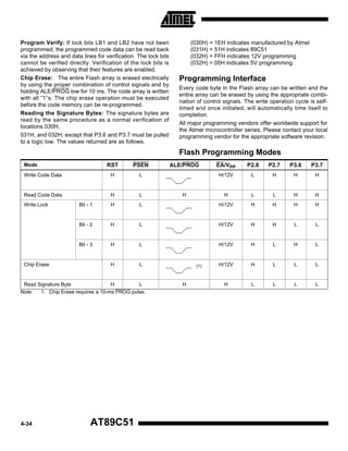


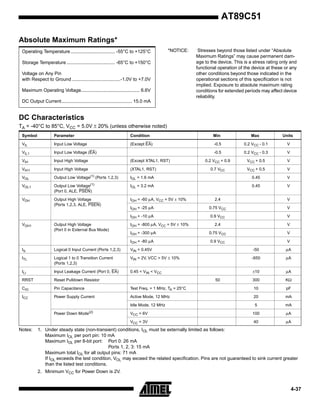
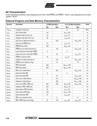


The AT89C51 is a low-power, high-performance 8-bit microcontroller with 4K bytes of flash memory. It has 32 I/O lines, two 16-bit timer counters, serial communication capabilities, and on-chip programming. The device operates between 0 and 24 MHz and has various power saving modes like idle and power down to reduce power consumption. It is compatible with the MCS-51 instruction set and provides a cost-effective solution for embedded applications.


