1. LH0002 Buffer
February 1995
LH0002 Buffer
General Description Features
The LH0002 is a general purpose buffer Its features make it Y High input impedance 400 kX
ideal to integrate with operational amplifiers inside a closed Y Low output impedance 6X
loop configuration to increase current output The symmetri- Y High power efficiency
cal output portion of the circuit also provides a low output Y Low harmonic distortion
impedance for both the positive and negative slopes of out- Y DC to 30 MHz bandwidth
put pulses Y Output voltage swing that approaches supply voltage
The LH0002 is available in an 8-lead TO-99 can The Y 400 mA pulsed output current
LH0002C is available in an 8-lead TO-99 and a 10-pin Y Slew rate is typically 200 V ms
molded dual-in-line package
Y Operation from g 5V to g 20V
The LH0002 is specified for operation over the b55 C to
a 125 C military temperature range The LH0002C is speci-
fied for operation over the 0 C to a 85 C temperature range
Applications
Y Line driver
Y 30 MHz buffer
Y High speed D A conversion
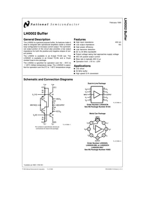
Schematic and Connection Diagrams
Dual-In-Line Package
TL H 5560 – 2
Order Number LH0002CN
See NS Package Number N10A
Metal Can Package
TL H 5560 – 1
Pin numbers in parentheses denote pin
connections for dual-in-line package
TL H 5560 – 3
Order Number LH0002H
LH0002H-MIL or LH0002CH
LH0002H 883
See NS Package Number H08D
Available per SMD 7801301
C1995 National Semiconductor Corporation TL H 5560 RRD-B30M115 Printed in U S A
2. Absolute Maximum Ratings (Note 3) Operating Ratings (Note 3)
If Military Aerospace specified devices are required Temperature Range
please contact the National Semiconductor Sales LH0002 b 55 C to a 125 C
Office Distributors for availability and specifications LH0002C 0 C to a 85 C
(Note 2) Thermal Resistance (Note 5)
Supply Voltage g 22V iJA H Package a 125 C W
Power Dissipation (Note 4) 600 mW iJC H Package a 75 C W
iJA N Package a 120 C W
Input Voltage (Equal to Power Supply Voltage)
Storage Temperature Range b 65 C to a 150 C
Junction Temperature
N Package a 150 C
H Package a 175 C
Steady State Output Current g 100 mA
Pulsed Output Current (50 ms On 1 sec Off) g 400 mA
Lead Temperature Soldering (10 seconds)
Metal Can 300 C
Plastic 260 C
ESD Rating (Note 6) 2 kV
Electrical Characteristics (Note 1)
Parameter Conditions Min Typ Max Units
Voltage Gain RS e 10 kX RL e 1 0 kX VIN e g 10V 0 95 0 97
Input Impedance RS e 200 kX VIN e g 1 0V RL e 1 0 kX 180 400 kX
Output Impedance VIN e g 1 0V RL e 50X RS e 10 kX 60 10 X
Output Voltage Swing RL e 1 0 kX VIN e g 12V g 10 g 11 V
Output Voltage Swing VS e g 15V VIN e g 12V RS e 50X RL e 100X TA e 25 C g 10 V
DC Output Offset Voltage RS e 300X RL e 1 0 kX g 10 g 30 mV
DC Input Bias Current RS e 10 kX RL e 1 0 kX g6 0 g 10 mA
Harmonic Distortion VIN e 5 0 Vrms f e 1 0 kHz 01 %
Rise Time RL e 50X DVIN e 100 mV 70 12 ns
Positive Supply Current RS e 10 kX RL e 1 0 kX a6 0 a 10 mA
Negative Supply Current RS e 10 kX RL e 1 0 kX b6 0 b 10 mA
Note 1 Specification applies for TA e 25 C with a 12V on Pins 1 and 2 b 12V on Pins 6 and 7 for the metal can package and a 12V on Pins 1 and 2 b 12V on
Pins 4 and 5 for the dual-in-line package unless otherwise specified The parameter guarantees for LH0002C apply over the temperature range of 0 C to a 85 C
while parameters for the LH0002 are guaranteed over the temperature range b 55 C to a 125 C unless otherwise specified
Note 2 Refer to RETS0002X for LH0002 military specifications
Note 3 Absolute Maximum Ratings indicate limits beyond which damage to the device may occur Operating Ratings indicate conditions for which the device is
intended to be functional but do not guarantee specific performance limits For guaranteed specifications and test conditions see the Electrical Characteristics
The guaranteed specifications apply only for the test conditions listed
Note 4 The maximum power dissipation is a function of maximum junction temperature (TJMax) total thermal resistance (iJA) and ambient temperature (TA) The
maximum allowable power dissipation at any ambient is PD e (TJMax b TA) iJA
Note 5 For operating at elevated temperatures the device must be derated based on the thermal resistance iJA and TJMax TJ e TA a PDiJA
Note 6 Human body model 1 5 kX in series with 100 pF
2
3. Typical Applications
High Current Operational Amplifier
TL H 5560 – 4
Line Driver
Previously called NH0002 NH0002C TL H 5560 – 5
Typical Performance Characteristics
Input Impedance
Frequency Response (Magnitude Phase) Supply Current
Positive Pulse Negative Pulse Input Bias Current
TL H 5560 – 7
3
5. Physical Dimensions inches (millimeters)
Metal Can Package (H)
Order Number LH0002H LH0002H-MIL LH0002H 883 or LH0002CH
NS Package Number H08D
5
6. LH0002 Buffer
Physical Dimensions inches (millimeters) (Continued)
Molded Dual-In-Line Package (N)
Order Number LH0002CN
NS Package Number N10A
LIFE SUPPORT POLICY
NATIONAL’S PRODUCTS ARE NOT AUTHORIZED FOR USE AS CRITICAL COMPONENTS IN LIFE SUPPORT
DEVICES OR SYSTEMS WITHOUT THE EXPRESS WRITTEN APPROVAL OF THE PRESIDENT OF NATIONAL
SEMICONDUCTOR CORPORATION As used herein
1 Life support devices or systems are devices or 2 A critical component is any component of a life
systems which (a) are intended for surgical implant support device or system whose failure to perform can
into the body or (b) support or sustain life and whose be reasonably expected to cause the failure of the life
failure to perform when properly used in accordance support device or system or to affect its safety or
with instructions for use provided in the labeling can effectiveness
be reasonably expected to result in a significant injury
to the user
National Semiconductor National Semiconductor National Semiconductor National Semiconductor
Corporation Europe Hong Kong Ltd Japan Ltd
1111 West Bardin Road Fax (a49) 0-180-530 85 86 13th Floor Straight Block Tel 81-043-299-2309
Arlington TX 76017 Email cnjwge tevm2 nsc com Ocean Centre 5 Canton Rd Fax 81-043-299-2408
Tel 1(800) 272-9959 Deutsch Tel (a49) 0-180-530 85 85 Tsimshatsui Kowloon
Fax 1(800) 737-7018 English Tel (a49) 0-180-532 78 32 Hong Kong
Fran ais Tel (a49) 0-180-532 93 58 Tel (852) 2737-1600
Italiano Tel (a49) 0-180-534 16 80 Fax (852) 2736-9960
National does not assume any responsibility for use of any circuitry described no circuit patent licenses are implied and National reserves the right at any time without notice to change said circuitry and specifications