Download to read offline


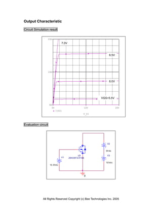


The document is a device modeling report for the 2SK3872-01S power MOSFET manufactured by Fuji Electric, detailing various circuit simulation results and parameters. It includes transconductance characteristics, capacitance measurements, gate charge dynamics, and diode characteristic data with associated error analysis. The findings illustrate simulation versus measurement comparisons, emphasizing performance metrics relevant for device application.


