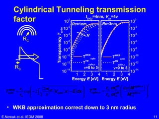
New Physical Model  for ultra-scaled  3D Nitride-Trapping Non-Volatile Memories E. Nowak , M. Bocquet, L. Perniola, G. Ghibaudo*, G. Molas, C. Jahan, R. Kies, G. Reimbold, B. De Salvo, F. Boulanger CEA-LETI, MINATEC
Outline Context and issues Tri-Gate memory cells Model for FN write/erase Data vs. model Scaling Conclusion E.Nowak et al. IEDM 2008
Nitride Tri-Gate devices Tri-Gate advantages: Increased Drive Current  Reduced Short Channel effects Nitride-trapping advantages: Lower operating voltages  Strong immunity  to oxide defects  Improved scalability Improved Program/ Erase characteristics E.Nowak et al. IEDM 2008
Literature Few recent models on the subject Si nanocrystal Tri-Gate   [Perniola L., IEDM 07] BE-SONOS Tri-Gate   [Hsu T.-H.,IEDM 07] Si nanocrystal Tri-Gate   [Nowak E., NVSMW 08] E.Nowak et al. IEDM 2008
Issue Corners in 3D structure appear critical Our approach Physics-based modeling of FN write/erase for Nitride-trapping Tri-Gate E.Nowak et al. IEDM 2008
Outline Context and issues Tri-Gate memory cells Model for FN write/erase Data vs. model Scaling Conclusion E.Nowak et al. IEDM 2008
Fabricated Devices SOI Charge-Trapping Tri-Gate non volatile memory W FIN  ~ 15 nm H FIN  ~ 20 nm SONOS / THiONOS stack E.Nowak et al. IEDM 2008 SONOS THiONOS
Outline Context and issues Tri-Gate memory cells Model for FN write/erase 1D modeling  Transmission factor Trapping modeling Data vs. model Scaling Conclusion E.Nowak et al. IEDM 2008
1D Model 1D potential & capacitance calculation for  planar  and  corner  regions Total programming window is weighted sum of each regions  E.Nowak et al. IEDM 2008 planar geometry cylindrical geometry [Nowak E., NVSMW 08] V G V D V S R C
Cylindrical Tunneling transmission factor WKB approximation correct down to 3 nm radius  E.Nowak et al. IEDM 2008 R C R C
Cylindrical Tunneling enhancement Transparency enhancement for small curvature radius Mandatory to use the exact shape of the barrier E.Nowak et al. IEDM 2008 R C R C
Trapping model Current fluxes: Tunneling Currents Electrons and holes included Capture/Emission with SRH and Poole-Frenkel electric field activation term Charge is solution of the differential system E.Nowak et al. IEDM 2008 Q n Q p Traps Electron currents Hole currents Channel Trapping  layer Control  Gate SiO 2 Si 3 N 4 SiO 2 HfO 2 Si TiN Δ E TRAP Channel Trapping  layer Control  Gate SiO 2 Si 3 N 4 SiO 2 HfO 2 Si TiN Δ E TRAP Q n Q p
Outline Context and issues Tri-Gate memory cells Model for FN write/erase Data vs. model SONOS vs. THiONOS Width dependence Temperature dependence   Scaling Conclusion E.Nowak et al. IEDM 2008
Experimental Results Better programming performances for THiONOS  Due to better coupling ratio thanks to HfO2 E.Nowak et al. IEDM 2008
Width dependence Δ V T  increases when reducing fin width Model predicts an higher impact of trapped charges at corners for smaller devices E.Nowak et al. IEDM 2008 V G =8V V G =12V V G =10V SONOS W FIN
Temperature impact on Write  (1/2) Similar write dynamics for different temperatures Lower saturation  Δ V T  level at high temperature E.Nowak et al. IEDM 2008 V G =8V V G =12V V G =10V SONOS
Temperature impact on Write  (2/2) J in-n  identical at both temperatures Δ V T  saturation at high temperature due to enhanced electron emission in nitride E.Nowak et al. IEDM 2008 T=25°C J in-n T=150°C J e-n J out-n SiO 2 Si 3 N 4 SiO 2 Si
Temperature impact on Erase  (1/2) Faster erase dynamics at high temperature E.Nowak et al. IEDM 2008 SONOS V G = -12V V G = -8V
Temperature impact on Erase  (2/2) Electron and hole currents must be considered during erase at high temperature E.Nowak et al. IEDM 2008 T=25°C SiO 2 Si 3 N 4 SiO 2 Si T=150°C J out-n J e-n J c-n J in-n
Outline Context and issues Tri-Gate memory cells Model for FN write/erase Data vs. model Scaling perspectives Conclusion E.Nowak et al. IEDM 2008
Scaling perspectives: HC-FET Reducing cell size    smaller  Δ V T  at saturation    faster dynamics E.Nowak et al. IEDM 2008 [D. Kwak et al, VLSI 07] // // // // //
Outline Context and issues Tri-Gate memory cells Model for FN write/erase Data vs. model Scaling Conclusion E.Nowak et al. IEDM 2008
Conclusion Physical model reproduces FN program/erase data of 3D nitride memory devices Corners modelled in cylindrical geometry Electron and hole currents considered Highlights: Write dynamics does not depend on temperature Erase performance is strongly dependent on temperature Scaling down HC-FET induces: Lower  Δ V T  at saturation Strongly enhanced write dynamics E.Nowak et al. IEDM 2008

Nowak IEDM'08

  • 1.
    New Physical Model for ultra-scaled 3D Nitride-Trapping Non-Volatile Memories E. Nowak , M. Bocquet, L. Perniola, G. Ghibaudo*, G. Molas, C. Jahan, R. Kies, G. Reimbold, B. De Salvo, F. Boulanger CEA-LETI, MINATEC
  • 2.
    Outline Context andissues Tri-Gate memory cells Model for FN write/erase Data vs. model Scaling Conclusion E.Nowak et al. IEDM 2008
  • 3.
    Outline Context andissues Tri-Gate memory cells Model for FN write/erase Data vs. model Scaling Conclusion E.Nowak et al. IEDM 2008
  • 4.
    Nitride Tri-Gate devicesTri-Gate advantages: Increased Drive Current Reduced Short Channel effects Nitride-trapping advantages: Lower operating voltages Strong immunity to oxide defects Improved scalability Improved Program/ Erase characteristics E.Nowak et al. IEDM 2008
  • 5.
    Literature Few recentmodels on the subject Si nanocrystal Tri-Gate [Perniola L., IEDM 07] BE-SONOS Tri-Gate [Hsu T.-H.,IEDM 07] Si nanocrystal Tri-Gate [Nowak E., NVSMW 08] E.Nowak et al. IEDM 2008
  • 6.
    Issue Corners in3D structure appear critical Our approach Physics-based modeling of FN write/erase for Nitride-trapping Tri-Gate E.Nowak et al. IEDM 2008
  • 7.
    Outline Context andissues Tri-Gate memory cells Model for FN write/erase Data vs. model Scaling Conclusion E.Nowak et al. IEDM 2008
  • 8.
    Fabricated Devices SOICharge-Trapping Tri-Gate non volatile memory W FIN ~ 15 nm H FIN ~ 20 nm SONOS / THiONOS stack E.Nowak et al. IEDM 2008 SONOS THiONOS
  • 9.
    Outline Context andissues Tri-Gate memory cells Model for FN write/erase 1D modeling Transmission factor Trapping modeling Data vs. model Scaling Conclusion E.Nowak et al. IEDM 2008
  • 10.
    1D Model 1Dpotential & capacitance calculation for planar and corner regions Total programming window is weighted sum of each regions E.Nowak et al. IEDM 2008 planar geometry cylindrical geometry [Nowak E., NVSMW 08] V G V D V S R C
  • 11.
    Cylindrical Tunneling transmissionfactor WKB approximation correct down to 3 nm radius E.Nowak et al. IEDM 2008 R C R C
  • 12.
    Cylindrical Tunneling enhancementTransparency enhancement for small curvature radius Mandatory to use the exact shape of the barrier E.Nowak et al. IEDM 2008 R C R C
  • 13.
    Trapping model Currentfluxes: Tunneling Currents Electrons and holes included Capture/Emission with SRH and Poole-Frenkel electric field activation term Charge is solution of the differential system E.Nowak et al. IEDM 2008 Q n Q p Traps Electron currents Hole currents Channel Trapping layer Control Gate SiO 2 Si 3 N 4 SiO 2 HfO 2 Si TiN Δ E TRAP Channel Trapping layer Control Gate SiO 2 Si 3 N 4 SiO 2 HfO 2 Si TiN Δ E TRAP Q n Q p
  • 14.
    Outline Context andissues Tri-Gate memory cells Model for FN write/erase Data vs. model SONOS vs. THiONOS Width dependence Temperature dependence Scaling Conclusion E.Nowak et al. IEDM 2008
  • 15.
    Experimental Results Betterprogramming performances for THiONOS Due to better coupling ratio thanks to HfO2 E.Nowak et al. IEDM 2008
  • 16.
    Width dependence ΔV T increases when reducing fin width Model predicts an higher impact of trapped charges at corners for smaller devices E.Nowak et al. IEDM 2008 V G =8V V G =12V V G =10V SONOS W FIN
  • 17.
    Temperature impact onWrite (1/2) Similar write dynamics for different temperatures Lower saturation Δ V T level at high temperature E.Nowak et al. IEDM 2008 V G =8V V G =12V V G =10V SONOS
  • 18.
    Temperature impact onWrite (2/2) J in-n identical at both temperatures Δ V T saturation at high temperature due to enhanced electron emission in nitride E.Nowak et al. IEDM 2008 T=25°C J in-n T=150°C J e-n J out-n SiO 2 Si 3 N 4 SiO 2 Si
  • 19.
    Temperature impact onErase (1/2) Faster erase dynamics at high temperature E.Nowak et al. IEDM 2008 SONOS V G = -12V V G = -8V
  • 20.
    Temperature impact onErase (2/2) Electron and hole currents must be considered during erase at high temperature E.Nowak et al. IEDM 2008 T=25°C SiO 2 Si 3 N 4 SiO 2 Si T=150°C J out-n J e-n J c-n J in-n
  • 21.
    Outline Context andissues Tri-Gate memory cells Model for FN write/erase Data vs. model Scaling perspectives Conclusion E.Nowak et al. IEDM 2008
  • 22.
    Scaling perspectives: HC-FETReducing cell size  smaller Δ V T at saturation  faster dynamics E.Nowak et al. IEDM 2008 [D. Kwak et al, VLSI 07] // // // // //
  • 23.
    Outline Context andissues Tri-Gate memory cells Model for FN write/erase Data vs. model Scaling Conclusion E.Nowak et al. IEDM 2008
  • 24.
    Conclusion Physical modelreproduces FN program/erase data of 3D nitride memory devices Corners modelled in cylindrical geometry Electron and hole currents considered Highlights: Write dynamics does not depend on temperature Erase performance is strongly dependent on temperature Scaling down HC-FET induces: Lower Δ V T at saturation Strongly enhanced write dynamics E.Nowak et al. IEDM 2008

Editor's Notes

  • #2 Thanks Mr. Chairman for the presentation. My name is Etienne Nowak and I will present you a work done at CEA-Leti Minatec, France. This work is entitled New Physical Model for ultra-scaled 3D Nitride Trapping Non Volatile Memories.