Download to read offline

![6. CONCLUSION:
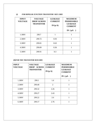
From table (i) we can see that, power transistor which we have used in our experiment are
active, because there are very minor difference between the applied voltage and the transistor
voltage drop. But from table (ii) we can see that the difference between supply voltage and the
transistor voltage drop is more than previous data. From the measuring data(ii), we observed
that the output leakage current Ico is more than the permissible leakage current.(3) So these
are the faulty transistors which are not applicable in high frequency circuit , because due to
this leakage current, the transistor switching circuit could not be run perfectly, causing
switching loss and leading to circuit failure. So from the mathematical equation is as
following we can measured the leakage current from any amplifier. From, Ohms law we know
that V=IR, so as per follow this law we can write
[Supply voltage (V) -x] / R = leakage current
[Where x = the transistor voltage drop]
Therefore, from that calculation we can easily measure the leakage current.
REFERENCES:
(1) JOURNAL OF REASERCH of National Standered Bureau of Standered C.-
Engineering & Instrumentation Vol-69C No-4
(2) PRICIPLES OF ELECTRONICS –BY V K MAHTA.-From-‘BJT Amplifier’.
(3) ELECTRONIC CIRCUITS-BY –DONALD A NYMEN-FROM-‘Transistor
Amplifier’.
(4) D. SHIN, J. KIM, and S. LEE, “Low-energy intra-task voltage scheduling using
static timing analysis,”.
(5) www.wekipedia.org.-‘Bipolar Junction Transistor’](https://image.slidesharecdn.com/c0d001c7-f45e-4da6-9bad-b5987b2c58a6-150811191500-lva1-app6892/85/208-EEI-49-6-320.jpg)

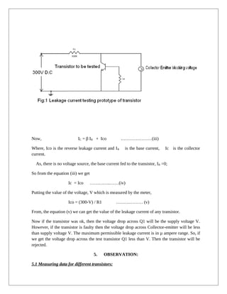
The document proposes a new method for detecting leakage current in bipolar junction transistors. It describes how leakage current increases over time as transistors age and degrade. It then presents a testing prototype that measures the voltage drop across a transistor under test to calculate its leakage current. The prototype applies a 300V supply to the transistor through a 1kΩ resistor. It then measures the voltage and uses Ohm's law to calculate the leakage current in μA. Testing several transistors showed some with negligible leakage current differences, while others exceeded the maximum permissible 1μA leakage, identifying them as faulty. The method provides an easy way to measure transistor leakage current for quality control.