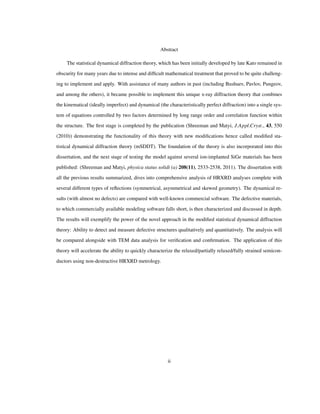
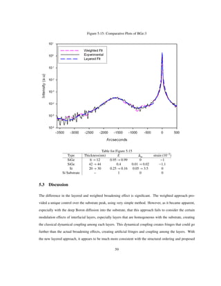
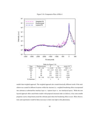
This dissertation applies a modified statistical dynamical diffraction theory (mSDDT) to analyze high-resolution x-ray diffraction (HRXRD) data from C-doped Si and SiGe heterostructures. The mSDDT improves upon previous statistical dynamical diffraction theory by incorporating weighted and layered broadening effects to better model defective and partially relaxed materials. Experimental HRXRD scans of SiGe samples are fitted using mSDDT and compared to commercial software. The results demonstrate mSDDT's ability to quantitatively characterize relaxed and defective semiconductor structures through non-destructive metrology.

![List of Figures
2.1 Illustrations of NMOS and PMOS respectively . . . . . . . . . . . . . . . . . . . . . . . . . . 3
2.2 Phase Diagram of SiGe [1] . . . . . . . . . . . . . . . . . . . . . . . . . . . . . . . . . . . . . 4
2.3 Strain Schematic Diagram [2] . . . . . . . . . . . . . . . . . . . . . . . . . . . . . . . . . . . 5
2.4 Diagram of misfit dislocation [3] . . . . . . . . . . . . . . . . . . . . . . . . . . . . . . . . . . 6
2.5 Common 60 dislocations in Si0.7Ge0.3 . . . . . . . . . . . . . . . . . . . . . . . . . . . . . . . 6
2.6 3C-SiC precipitates (marked by p) [4] . . . . . . . . . . . . . . . . . . . . . . . . . . . . . . . 8
2.7 Phase Diagram of Si-C . . . . . . . . . . . . . . . . . . . . . . . . . . . . . . . . . . . . . . . 9
2.8 An Example of Material of Interest: graded SiGe . . . . . . . . . . . . . . . . . . . . . . . . . 10
2.9 Graded SiGe with Mosaic Model . . . . . . . . . . . . . . . . . . . . . . . . . . . . . . . . . . 11
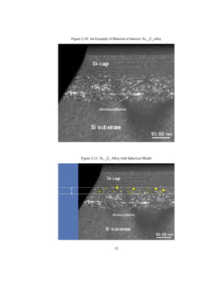
2.10 An Example of Material of Interest: Si1 yCy alloy . . . . . . . . . . . . . . . . . . . . . . . . . 12
2.11 Si1 yCy Alloy with Spherical Model . . . . . . . . . . . . . . . . . . . . . . . . . . . . . . . . 12
3.1 The simple cube lattice is shown along 001 direction on left, while one on right is in [111]
direction . . . . . . . . . . . . . . . . . . . . . . . . . . . . . . . . . . . . . . . . . . . . . . . 14
3.2 The diamond lattice is shown along 001 direction on left, while one on right is in [111] direction 14
3.3 The miller planes of (004), (113), and (224) are shown respectively within the diamond unit cell
to illustrate the different reflections of diffraction being characterized in HRXRD in this study. . 14
3.4 Bragg’s Law . . . . . . . . . . . . . . . . . . . . . . . . . . . . . . . . . . . . . . . . . . . . . 16
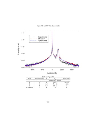
3.5 Sample Rocking Curve . . . . . . . . . . . . . . . . . . . . . . . . . . . . . . . . . . . . . . . 16
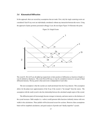
3.6 Single Events . . . . . . . . . . . . . . . . . . . . . . . . . . . . . . . . . . . . . . . . . . . . 17
3.7 Bulk 004 GaAS Rocking Curve [5] . . . . . . . . . . . . . . . . . . . . . . . . . . . . . . . . . 19
3.8 Bulk to Thin Film Structure . . . . . . . . . . . . . . . . . . . . . . . . . . . . . . . . . . . . . 20
3.9 Multiple Events . . . . . . . . . . . . . . . . . . . . . . . . . . . . . . . . . . . . . . . . . . . 21
3.10 LEPTOS snapshot . . . . . . . . . . . . . . . . . . . . . . . . . . . . . . . . . . . . . . . . . . 22
3.11 Dynamical Model vs. relaxed sample . . . . . . . . . . . . . . . . . . . . . . . . . . . . . . . 24
4.1 Replication of Bushuev’s work [6] . . . . . . . . . . . . . . . . . . . . . . . . . . . . . . . . . 32
4.2 Illustration of Mosaic model . . . . . . . . . . . . . . . . . . . . . . . . . . . . . . . . . . . . 34
4.3 Examples of M effects . . . . . . . . . . . . . . . . . . . . . . . . . . . . . . . . . . . . . . . 35
vi](https://image.slidesharecdn.com/2af25ca4-a567-429d-a0c9-5d02c7cc9e50-170206043027/85/20120112-Dissertation7-2-6-320.jpg)
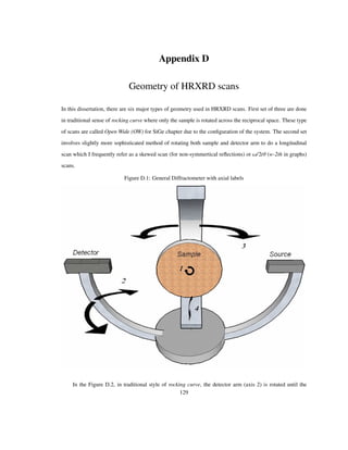
![discussion and overview of scaling laws as it applies to scaling to micro/nanoworld, please refer to this
work [7].
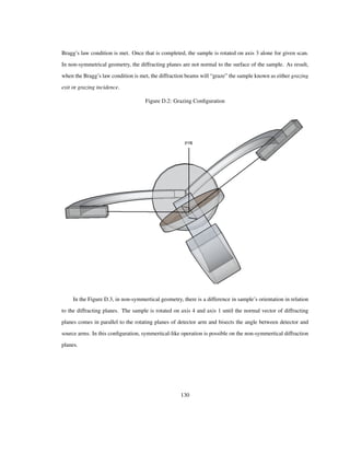
The issues surrounding defects within the semiconductor will be discussed more in-depth in next several
chapters. The basic idea is that if the structure, especially the thin-film heterostructures comprised of epitaxial
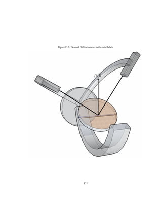
layer of few atoms thick, will be extremely sensitive to minor infractions of crystalline quality of substrate or
the interface between the layers.
The appeal of using X-rays as a metrological tool are many:
1 X-rays wavelengths range is approximately 10 to 0.01 nanometers. One of the commonly used radia-
tion sources in X-ray diffraction (CuΚΑ
) is approximately 0.15nm.
2 There are affordable high-intensity X-ray sources available for fab installations, and the academic
laboratories. The availability of lab tools (i.e. not synchrotron based) with high intensity X-ray sources
are relatively recent.
3 X-ray methods provides an excellent high-throughout metrological tool. The process for X-ray diffrac-
tion characterizations are completely non-destructive and does not require any sample preparations.
The relative ease of using X-ray tool for quick semiconductor tool for fabrication plants focused on
quality of crystalline substrate/films is very appealing. The issues are that the currently known available
tools are relatively limited to powder analysis, or else relatively perfect crystalline structures. The common
application of general XRD is to characterize the unknown materials by powder method, and to identify the
diffraction peaks based on material databases. For thin-films, the HRXRD metrology is commonly used
to study the strain of the epitaxial layers. However, there is currently no commercially available or known
approaches at this time to analyze the layers that are partially to fully relaxed.
This dissertation research addresses the need for the ability to characterize quantitatively and qualita-
tively the modern-day electronics that manifest neither perfectly crystalline or ideally imperfect crystals.
2](https://image.slidesharecdn.com/2af25ca4-a567-429d-a0c9-5d02c7cc9e50-170206043027/85/20120112-Dissertation7-2-12-320.jpg)
![Chapter 2
Examples of Materials of Interest
Thin-film heterostructure such as Si/SiGe and Si/Si:C will be presented in this section as part of introduction
to the basic structure in many of the modern-day microelectronics. These types of basic structures are key
components where electronic properties can be manipulated by strain or relaxation of the epitaxial layer(s)
on the substrate. For example, in epitaxial layers of SiGe, it can be used to enhance the hole mobility in
pMOS, while SiC can be used to enhance electron carrier mobility in nMOS type devices (Figure 2.1).
Figure 2.1: Illustrations of NMOS and PMOS respectively
2.1 Introduction of SiGe
The number of the publications on SiGe (Silicon Germanium) is large. The suggested listing of reading is
wholly incomplete and only serve as a starting point, along with pointers in current research interests in SiGe
technology:
• A patent using Schottky barrier diode on a SiGe Bipolar complementary metal oxide semiconductor
(BiCMOS) wafer for 1.0 THz or above cutoff frequency based on epitaxial layer [8]
3](https://image.slidesharecdn.com/2af25ca4-a567-429d-a0c9-5d02c7cc9e50-170206043027/85/20120112-Dissertation7-2-13-320.jpg)
![Figure 2.2: Phase Diagram of SiGe [1]
• A throughout review article covering SiGe applications in complementary metal oxide semiconductor
(CMOS) and heterojunction biploar transistor (HBT) [2]
• An article addressing the issues of relaxation of SiGe in development for p-type metal oxide semicon-
ducto field effect transistor (PMOSFET) [9]
• Study of selective epitaxial growth of Boron doped SiGe for PMOSFET [10]
• Another paper focusing on millimeter wave transistors, using selective epitaxial growth methods [11]
• In-depth study of SiGe strain relaxation based on different crystal orientations [12]
• Study of highly strained SiGe epi-layer on silicon on insulator (SOI) for PMOSFET applications [13]
• Interesting analysis of SiGe scratch resistance [14]
• Discusses the fully-relaxed SiGe on SOI [15]
There are several reasons why the wafers composed of bulk Silicon (Si) are central to the semiconductor
industry. The ease and availability of near-perfect boules for Si wafers can be commercially grown and
provide to be the cheapest material for electronics. The SiGe with the variable of Ge as function of x in
Si1 xGex allows for variable strain based on the Ge percentage of the film. For illustration, please see the
phase diagram (Figure 2.2). Regardless of composition, the crystalline structure will remain diamond. The
lattice parameter relationship between Ge (which has 4.2% larger lattice constant) and Si can be reasonably
modeled by Vegard’s law [16]. Vegard’s law approximates that at constant temperature, a linear relationship
exists between crystal lattice constant and the alloy’s composition of the elements.
4](https://image.slidesharecdn.com/2af25ca4-a567-429d-a0c9-5d02c7cc9e50-170206043027/85/20120112-Dissertation7-2-14-320.jpg)
![Relaxation and Strain of SiGe
Figure 2.3: Strain Schematic Diagram [2]
Using the modified Figure 2.3 from the article [2], it is observable that the relationship between com-
pressive strain occurs when the epitaxial layer’s lattice parameter is larger than the substrate (a) to (b), and
if the epitaxial layer’s lattice parameter is smaller than substrate that it will undergo tensile strain (c) to (d).
In both cases, the epitaxial layer experience tetragonal lattice distortion. The epi-layer can be strained up to
a point, depending on the thermodynamic equilibrium, where the energy of strain exceeds the energy asso-
ciated with development of defects. The critical thickness of the epitaxial layer exists where the energy of
defect development will exceed the strain’s energy. One of models that attempt to predict the critical thick-
ness based on propagation of threading dislocation is known as Matthews-Blakeslee model [17–19]. This
critical thickness parameter depends on many growth parameters: type of growth (MBE, CVD, etc), types
of chemical reactions, percentage of Ge incorporation, growth rate and temperature of the process. There
are several models designed to predict the critical thickness explained in the review article [2]. The most
common defect development to relieve the strain for SiGe is known as A/2 < 110 > 60 dislocation type.
This threading dislocation is due to misfit dislocation (see Figure 2.4).
5](https://image.slidesharecdn.com/2af25ca4-a567-429d-a0c9-5d02c7cc9e50-170206043027/85/20120112-Dissertation7-2-15-320.jpg)
![Figure 2.4: Diagram of misfit dislocation [3]
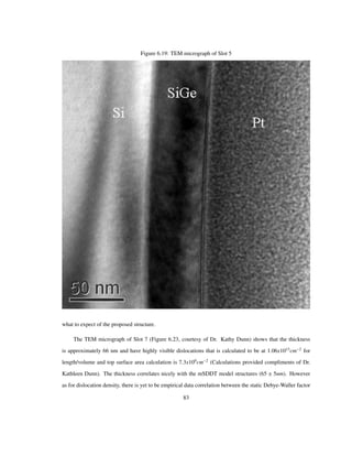
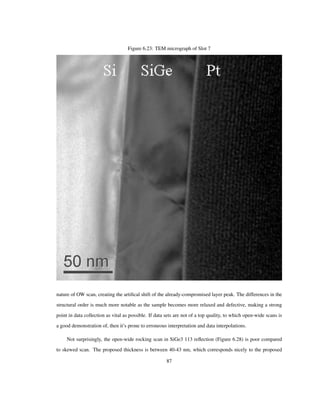
For additional illustration, please refer to Figure 2.5, which is TEM micrograph of 170 nm thick relaxed
Si0.7Ge0.3 layer on Si Substrate. The 60 dislocations are visible as triangular shaped lines, and the dark line
exemplifies the fully defective interface between layer and the substrate.
Figure 2.5: Common 60 dislocations in Si0.7Ge0.3
The one of the current challenges is to increase the strain of the SiGe layer, further enhancing the hole
mobility. However, as the germanium content is increased to create more strain, it becomes more likely to
6](https://image.slidesharecdn.com/2af25ca4-a567-429d-a0c9-5d02c7cc9e50-170206043027/85/20120112-Dissertation7-2-16-320.jpg)
![create more dislocations and defects.
2.2 Introduction of SiC
This section on SiC is included for an additional illustration of materials that would be ideal candidate for
this thesis work.
• A study of CMOS with SiGe and SiC source/drain stressors [20]
• SiC for MOSFET applications [21–23]
• Study of electron mobility [23]
• Micro-elecromechanical systems [24]
• 1 T-DRAM Flash Memory [25]
• N-type MOS devices [26,27]
In addition, there are many other applications of carbon incorporation such as carbon implantation for
transient enhanced diffusion barriers [28] and controlling the strain in SiGe by carbon incorporation [29–31]
There are several crystal types of SiC. However, there are only one that has cubic structure type called
3C-SiC also called Β-SiC. This “cubic SiC” has the zincblende structure, and is the structure which grows on
the Si substrates (which has diamond structure). A excellent review [32], along with other papers, [33, 34],
describes the mismatch between Si Substrate and the Β-SiC to be 20% in lattice parameters and 8% in thermal
expansion coefficients. The mismatch between these materials is extreme for an epitaxially thin (and perfect)
Β SiC layers on Si substrates. These types of Β SiC films are usually several micrometer thick, with high
defect contents within the interface layers.
Instead, an alternative tensile-strained Si layer with varying substitutional carbon content incorporation
may be used. The growth of these initial layers does not have a specific crystalline structures, and the carbon
substitutions are randomized. The literature commonly refer these thin films as Si1 xCx with x as percentage
of carbon incorporation of the given layer. As the incorporation of the carbon increases (substitution of Si
atoms with C atoms in the lattice), the tensile stress of layer increases. Even though there is reported 7%
carbon incorporation based on MBE growth [30], the limit of 2% is generally assumed due to low solubility
of C in Si (10 4
% at 1400 C) [27].
7](https://image.slidesharecdn.com/2af25ca4-a567-429d-a0c9-5d02c7cc9e50-170206043027/85/20120112-Dissertation7-2-17-320.jpg)
![The challenge in carbon incorporation where the greater strains also usually mean greater chances of
defect development warrants more in-depth study. For example, Berti et al [35] discusses the deviations of
Vegard’s rule (linear interpolation) in regard to lattice parameters in relationship with carbon incorporation.
Kovats et al [36] discusses the issue of Β SiC precipitation growing within the Si1 xCx layer (See Figure 2.6).
Clearly, there is fine line between carbon incorporation for Si lattice manipulation (tensile-strained Si layer
on Si substrate, for instance) instead of forming actual Β SiC crystals with numerous defects. The main
objective is to form a pseudomorphically thin Si1 xCx layer with specific strain profile, without defects.
Figure 2.6: 3C-SiC precipitates (marked by p) [4]
The challenge remains in the fact that only at exactly 50% carbon composition that a single phase exists
in equilibrium. The non-50% carbon composition is two phased (Α-SiC for less than 50% and Β-SiC for more
8](https://image.slidesharecdn.com/2af25ca4-a567-429d-a0c9-5d02c7cc9e50-170206043027/85/20120112-Dissertation7-2-18-320.jpg)
![than 50%). These phases are illustrated in the Si-C phase diagram (Figure 2.7.
Figure 2.7: Phase Diagram of Si-C
http://www.ioffe.ru/SVA/NSM/Semicond/SiC/thermal.html
Growth Methods
Molecular beam epitaxy (MBE) can be used [30, 37], however the growth rate is too slow in MBE for the
fabrication process for industrial applications. A novel growth procedure called solid phase epitaxy (SPE)
was proposed by Strane [29, 38]. Regardless, chemical vapor deposition (CVD) appears to be the most
practical and economical growth method for this study. However, with the conventional CVD processes, the
temperature is relatively high 1300 C , making it unsuitable for semiconductor processing. There are
variations of CVD method such as UHVCVD (ultra-high vacuum chemical vapor deposition) [22], reduced
pressure chemical vapor deposition [26, 27], and plasma enhanced CVD (PECVD) [39–48] that allows for
the depositions to occur at much lower temperature, making it suitable for semiconductor processing.
9](https://image.slidesharecdn.com/2af25ca4-a567-429d-a0c9-5d02c7cc9e50-170206043027/85/20120112-Dissertation7-2-19-320.jpg)
![2.3 Characterization of Materials of Interest
This section focuses on the potential of the dissertation’s work. The modified Statistical Dynamical Diffrac-
tion (mSDDT), which has been developed as result of this thesis, provides the opportunity to specifically
characterize given materials based on several parameters:
• thickness
• strain
• composition
• long order
• type of defect
Two extreme examples to which this work can be applied to in respect to the materials of interest. The
graded SiGe (Figure 2.8) from the useful introductory website [1] provides an useful analogy.
Figure 2.8: An Example of Material of Interest: graded SiGe
As part of the mSDDT model, the correlation length (which will be described in depth in later sections)
uses mosaic blocks as a defect model. In this approach, the proposal is to characterize the dislocations
10](https://image.slidesharecdn.com/2af25ca4-a567-429d-a0c9-5d02c7cc9e50-170206043027/85/20120112-Dissertation7-2-20-320.jpg)
![as a mosaic blocks that will diffract at angular deviation. With the inclusion of defect structure model,
mSDDT can predict nominal structures such as strain, composition, and thickness of given layer with much
more accuracy and precision than what is currently available. In Figure 2.9, the proposed mosaic blocks
are superimposed on the Figure 2.8 for illustrative purpose, where the proposed model will attempt to predict
given thickness of layer with average angular deviation of mosaic blocks and the overall order of the structure
each layer as represented by white lines and arrows.
Figure 2.9: Graded SiGe with Mosaic Model
Another example (Figure 2.10) based on Berti et al work [49]: Si1 yCy alloy with carbon precipitates.
Another possible model for correlation length, spherical model, is superimposed on the figure (Figure 2.11).
Again, the proposed model would be able to extract nominal structure information: strain, composition, and
thickness of given layer (represented by white lines and arrows) with ease. Meanwhile, the ultimate goal is
to be able to accurately predict the overall structure of defects: long order and the average sphere radii size.
11](https://image.slidesharecdn.com/2af25ca4-a567-429d-a0c9-5d02c7cc9e50-170206043027/85/20120112-Dissertation7-2-21-320.jpg)
![Chapter 3
X-Ray Diffraction Fundamentals
It is grave injustice to discuss the X-ray diffraction theory in a single thesis, and in attempt to counter that
limitation, several books will be briefly discussed. One of the modern comprehensive book on dynamical
theory, even providing a brief overview of SDDT as proposed by Kato is discussed by Dynamical Theory of
X-ray Diffraction [5]. The classical texts that should prove to be extremely useful for students in this field:
X-Ray Diffraction [50] which is mostly kinematical in treatment, and classical text on dynamical treatment
by Theory of X-Ray Diffraction in Crystals [51]. For application-driven approach, the HRXRD treatment is
discussed in High Resolution X-ray Diffractometry and Topography [52], and to a different approach (more
focused on defects), High-Resolution X-Ray Scattering [53]. For more textbook feel, Elements of X-ray
Diffraction [54] or Elements of Modern X-ray Physics [55] may be suitable. Finally, but one of the most
indispensable resource is International Tables of Crystallography: Mathematical, Physical and Chemical
Tables [56] which contains many necessary references for work in this field.
3.1 Crystallography
A discussion of X-ray diffraction requires some familiarity with crystallography which is the study of the
crystalline materials. One of the good introductory texts, The Basics of Crystallography and Diffraction [57]
can be referred for more in-depth treatment. The crystals are defined based on repeatable patterns of atomic
arrangements. There are limited geometric selections to what kind of pattern can be formed, but materials
can usually be identified based on its atomic (molecular, or even compounds) structures. Starting with one of
most basic structure (Figure 3.1) which is a box of single atom basis with each corner occupied by 1/8 of the
atom.
Silicon, one of the most commonly used material for integrated circuits has the diamond lattice Fig-
ure 3.2. In addition, the SiGe and SiC will also ideally have the same structure (i.e. fully strained layers).
Due to these diamond structures, three main reflections of these planes will be used: (004),(113) and (224)
illustrated in Figure 3.3.
13](https://image.slidesharecdn.com/2af25ca4-a567-429d-a0c9-5d02c7cc9e50-170206043027/85/20120112-Dissertation7-2-23-320.jpg)
![Figure 3.1: The simple cube lattice is shown along 001 direction on left, while one on right is in [111]
direction
Figure 3.2: The diamond lattice is shown along 001 direction on left, while one on right is in [111] direction
Figure 3.3: The miller planes of (004), (113), and (224) are shown respectively within the diamond unit cell
to illustrate the different reflections of diffraction being characterized in HRXRD in this study.
Illustrations created by Crystallographica [58], available at
http://www.oxcryo.com/software/crystallographica/crystallographica/
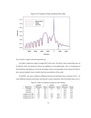
3.2 Scattering of X-Rays
The scattering of the X-rays, which is the basis of the X-ray diffraction, depends on the numbers of the
electrons available for scattering within an atom. Each atom has different scattering amplitude known as
the atomic scattering factor ( fn) that depends on numbers of electrons and the angle of scattering. The
crystalline structure has identical units of given geometric pattern of atomic basis (i.e. Si in diamond lattice)
14](https://image.slidesharecdn.com/2af25ca4-a567-429d-a0c9-5d02c7cc9e50-170206043027/85/20120112-Dissertation7-2-24-320.jpg)
![in a repeating matrix that could constructively or destructively amplify the electromagnetic waves. For these
amplification calculations, the structure factor (FHKL) is used. The structure factor sums up the vectors of the
atomic positions in a given unit cell, angles of incoming and outgoing X-ray waves, and the atomic scattering
factor into a single value.
FHKL
N
n 0
fn exp 2Πi hun kvn lwn (3.1)
where fn is atomic scattering factor, and h, k, l represents the reflection type (the angle of the diffraction)
with respect to the fractional coordinations of nth atom (un, vn, wn) in given unit cell. For a very rough
approximation, it could be stated that the intensity of the given reflection is proportional to the square of the
structure factor.
In a different perspective, the mathematical treatment incorporates the electron density of the material
(commonly denoted as Ρ r ) to calculate the dielectric susceptibility or polarizability. The Fourier expansion
of the polarizability has same format as the structure factor [5].
ΧHKL
RΛ2
FHKL
ΠV
(3.2)
where ΧHKL is polarizability of the given material, R - classical radius of the electron, X-ray wavelength as Λ,
and V as volume of the unit cell.
In fact, the polarizability is directly proportional to the structure factor, but also may incorporate addi-
tional parameters such as anomalous dispersion corrections (also known as Hönl corrections [59]) and the
Debye-Waller factor. Special note must be made here to signify the term, Debye-Waller factor. In classi-
cal terms, this factor is a temperature factor, based on atomic vibrations. In later sections on the statistical
dynamical diffraction theory, there is a new parameter formally called static Debye-Waller factor. The math-
ematical format is very similar, but is not temperature related or to the classical employment of Debye-Waller
factor.
3.3 Fundamentals of X-ray Diffraction
Crystalline structures exhibits diffraction properties that can be described by well-known Bragg’s Law illus-
trated in Figure 3.41
.
1The figure was modified from CNSE course presentation materials
15](https://image.slidesharecdn.com/2af25ca4-a567-429d-a0c9-5d02c7cc9e50-170206043027/85/20120112-Dissertation7-2-25-320.jpg)
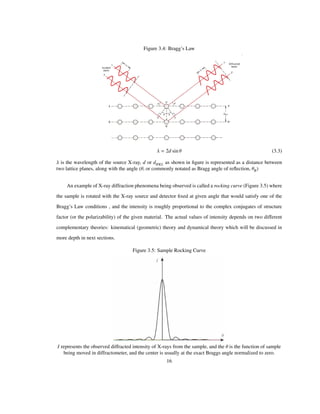
![The full width at the half maximum (FWHM) is the accepted standard of measuring the width of the
diffraction. In the kinematical theory, FWHM is inversely proportional to the total thickness of the sample
being irradiated. In addition, the total observed intensity will also increase in proportion to the thickness
squared. As result, the observed intensity, according to the current theory, will progressively become a delta
function which is not accurate portrayal of XRD of thick samples ( microns).
3.5 Dynamical Diffraction
For the bulk near-perfect crystals, the dynamical diffraction theory offers an electromagnetic solution with
Maxwell’s equations describing the interactions between the X-rays and the materials. One of the main
difference between the kinematical and dynamical diffraction theories is the coupling between incident and
diffracted waves within the material. The illustration, Figure 3.9, show shaded triangle abc of coupling
waves. The dynamical solution considers the multiple events simultaneously, integrating the interactions of
waves (both incident and diffracted waves) within the matrix of the given boundary conditions. For a bulk
sample, the classical dynamical solution is very straightforward:
Ih Η Sign nr Η2
1 (3.4)
where Ih is the observable intensity of rocking curve. Based from Authier’s book [5], Figure 3.7 is a traditional
rocking curve based on bulk material in 004 reflection of GaAs (Gallium arsenide). The equation 3.4 is
basically just a function of deviation parameter, Η.
Η
Θ ΘB sin 2ΘB Χo
ΧhΧh
(3.5)
where the ΘB is the Bragg angle of given material, the polarizability (represented by Χ) in directions (incident
(o), diffracted (h), and back-diffracted (h), and the angular scan (Θ). For much more in-depth reading on the
classical dynamical theory, the review article by Batterman and Cole [59] is recommended. For the discussion
of the wave interactions within the crystalline matrix, please refer to an article by Slater [60].
The dielectric susceptibility is the integral part of the Maxwell’s equations, and is assumed to be con-
stant. This primary assumption is one of the pivotal issues in classical dynamical theory, and unfortunately
is the major weakness in constructing solutions for modern structures such as thin film technology. The il-
lustration (Figure 3.8 shows the schematics behind the basic dynamical diffraction modelling. The layers of
18](https://image.slidesharecdn.com/2af25ca4-a567-429d-a0c9-5d02c7cc9e50-170206043027/85/20120112-Dissertation7-2-28-320.jpg)
![Figure 3.7: Bulk 004 GaAS Rocking Curve [5]
The two plots are represented by two different calculations: the square (dotted) plot represents ideally non-
absorbing crystal, while the solid plot represents a realistic absorbing crystal rocking curve of GaAs.
the structure (whether it is abrupt, transitional, etc) determine the definition of the polarizability. Instead of
a constant for the electron density, the polarizability becomes a function of depth. In addition, the recursion
calculation is necessary to modulate the diffraction through different electron densities (i.e. layers). As result,
a different method of dynamical calculations is necessary.
Tapuin-Takagi Model
Fortunately, a modification of the dynamical theory by Takagi and Tapuin [61–63] resolved the issue of
functional polarizability by generalizing the solution to accept a small fluctuations. The proposed solution
did use functional polarizability, however dropped terms that are considered small enough, simplifying the
equations enough for generalized solution for slightly distorted crystals.
There are several variations of the Tapuin-Takagi (T-T) equations being used in literature. Two common
19](https://image.slidesharecdn.com/2af25ca4-a567-429d-a0c9-5d02c7cc9e50-170206043027/85/20120112-Dissertation7-2-29-320.jpg)
![Figure 3.8: Bulk to Thin Film Structure
The transition between bulk to thin film is dramatically different for classical dynamical modeling. The
classical diffraction profile of layered structure, along with possible slight imperfect interface in between
proves to be impractical.
formats of computation-friendly equations are partial differential equations (PDE) or Reimann sum, and
many authors have developed their own nomenclature of T-T equations. In this dissertation, the PDE format
in Bushuev’s definitions and notations are used [6, 64]. For illustration, the Appendix A compares two
different approaches by two different authors: A well-known dynamical treatment by Bartels et al [65] and
the background of this thesis approach [6,64].
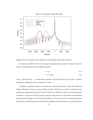
3.6 Applications of High Resolution X-ray Diffraction
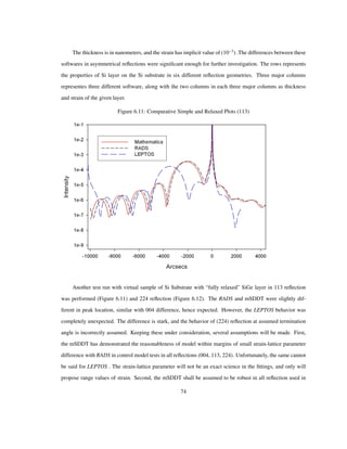
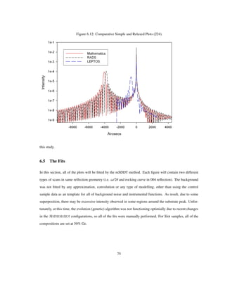
There are several commercial software that provides tools for analyzing XRD data such as LEPTOS [66] and
RADS [67]. In this Figure 3.10, a snapshot of LEPTOS is used to illustrate what the software is designed to
perform in respect to XRD data anaylsis.
The high-resolution aspect (HRXRD) allows for much higher resolution that only spans few arcseconds
in the reciprocal space with much greater detail than a typical XRD scans. The fringes seen around the
layer peak is proportional to the thickness of the layer, and the distance between substrate and layer peak
determines the lattice difference (strain and composition). Other software commonly offers similar type of
tools, and they all are based on variants of dynamical theory. The dissertation will discuss the differences and
comparisons between these software in later chapters.
20](https://image.slidesharecdn.com/2af25ca4-a567-429d-a0c9-5d02c7cc9e50-170206043027/85/20120112-Dissertation7-2-30-320.jpg)
![Figure 3.9: Multiple Events
The shaded triangle abc represents area of imaginary boundary conditions for Maxwell’s classical dynamical
solution that incorporates interactions between incident and diffracted waves. The z represents the depth
starting at surface of sample.
3.7 Shortcomings and Challenges in the X-ray Diffraction Theories
Many critical materials and structures (such as lattice-mismatched semiconductor heterostructures, or ma-
terials modified by ion implantation or impurity diffusion processing) are characterized by the presence of
process-induced structural defects. These materials cannot be modeled by the conventional model of dynami-
cal theory of a nearly-perfect single crystal layers on a perfect single crystal substrate. Alternative approaches
to the dynamical theory approach include the work of Servidori [68] and Shcherbachev and coworkers [69].
In both cases, the authors explicitly incorporate the effects of structural defects via the inclusion of a static
Debye-Waller factor that modulates the dynamically diffracted amplitude.
This approach is highly effective in providing quantitative modeling of structures that are only slightly
21](https://image.slidesharecdn.com/2af25ca4-a567-429d-a0c9-5d02c7cc9e50-170206043027/85/20120112-Dissertation7-2-31-320.jpg)
![Figure 3.10: LEPTOS snapshot
perturbed from the ideally perfect dynamic diffraction limit; however, in heavily defected materials, it would
be expected to fail because there is no explicit mechanism for including the effects of kinematic scattering
that would be generated in the defective layers. The other extreme – employing a fully kinematical cal-
culation for partially defective crystalline structures – would be expected to experience limitations if either
the substrate or any layers in a multilayer structure would have strong dynamical diffraction behavior. A
“semi-kinematical” approach developed by authors such as Speriosu [70, 71] uses dynamical calculations
for the substrate, while applying a purely kinematical model based on Zachariasen [51] for layer calcula-
tions. Clearly, this method presumes that the substrate and layer diffract solely according to the dynamic and
kinematic theories, respectively. In a real material such as an industrially-relevant semiconductor epitaxial
heterostructure, this presumption of crystalline perfection (or lack thereof) may not be warranted; indeed, the
degree of crystalline perfection may not be known a priori at all.
A more sophisticated approach involves the analytical calculation of the defect scattering and to in-
corporate this into a full modeling of the total diffracted intensity. A general treatment for calculating the
kinematic intensity scattered by statistically distributed defects in nearly perfect crystals has been developed
by Krivoglaz [72]. This approach has been applied in several studies to a variety of different semiconductor
systems [73–76]. A fully quantitative analysis via modeling of the defect scattering typically requires a full
knowledge of the characteristics of the defects in the diffracting crystal; unfortunately this is typically not the
case in many applications-driven uses of high resolution X-ray methods, such as in metrology and materials
22](https://image.slidesharecdn.com/2af25ca4-a567-429d-a0c9-5d02c7cc9e50-170206043027/85/20120112-Dissertation7-2-32-320.jpg)
![evaluation.
An alternative method used by Molodkin and several other authors [77–81] developed a “generalized
dynamical theory” that is based on using perturbation theory to solve fluctuating polarizability in momentum
space. This model bypasses limitations of kinematical model of small defect sizes by including dynamical
effects of defects, and redistribution of the dynamical scattering within the material. The initial development
focused on single crystal model [77,79,80], and the multi-layer treatment [78] used specific type of defects
within the substrate, not in the layers. Their defect model is designed for specific defects and incorporate the
static Debye-Waller factors and absorption effects.
In applications such as semiconductor manufacturing, one often encounters crystalline materials that
contain a complex defect structure. In these cases, detailed modeling of scattering via defect simulation is
not possible, due to the fact that the details of the defect structure will not be known. Despite this, the fact
that these single crystal materials are structurally-defective will be evident by their deviation from perfect-
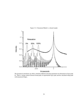
crystal dynamic theory. Figure 3.11 illustrates a typical example of an X-ray rocking curve recorded from a
thick (approximately 170 nm) epitaxial layer of highly lattice-mismatched Si0.70Ge0.30/Si. The figure shows
rocking curves calculated from dynamical simulation; the lack of agreement is anticipated due to the high
density of structural defects in a thick, fully strain-relaxed Si1 xGex/Si epitaxial system. The relaxation
parameter may be extracted from the layer’s peak position in relationship to the substrate peak with current
dynamical theory but several other parameters such as thickness and extent of damage cannot be extracted
using only conventional dynamical theory. The fringes that are commonly observed in near-perfect samples
depends on dynamical coupling that proportionally decrease in respect to the extent of damage due to defect
scattering. In addition, the defective structures exhibits broadening effects on the layer and substrate peaks.
Depsite many challenges in the X-ray theoretical models, it is clear that the experimental XRD/HRXRD
scans are capable of detecting full range of near-perfect crystalline layers that are strained to highly mis-
matched and relaxed layers. The range of extreme limits is currently dominated by either dynamical or
kinematical theory, with a massive gap in the middle. This gap is now being addressed with a novel approach
that combines the extremes into a unified theory of statistical dynamical diffraction theory (SDDT).
23](https://image.slidesharecdn.com/2af25ca4-a567-429d-a0c9-5d02c7cc9e50-170206043027/85/20120112-Dissertation7-2-33-320.jpg)
![Chapter 4
Fundamentals of Statistical Dynamical Diffraction Theory
4.1 Introduction to Statistical Dynamical Diffraction Theory
In a series of papers, Kato developed the basis for the statistical dynamical diffraction theory (SDDT), which
incorporates both types of scattering that Kato called incoherent (kinematical/diffuse), and coherent (dy-
namical) scattering [82–87]. Kato modified the conventional formalism in both kinematical and dynamical
theories to include effects of defect scattering by adding statistical averaging of lattice displacement, intro-
ducing two new parameters: a static Debye-Waller factor E, and a complex correlation length Τ.
Kato’s work only provided a method for determining the integrated intensity in the transmission Laue
diffraction geometry; this limited its applicability to technologically-important systems such as the analysis
of thin films on thick substrates in a reflection (Bragg) geometry. Bushuev [6,64] expanded Kato’s theory by
using a plane-wave approximation (rather than Kato’s spherical wave approach) and modifying the Tagaki-
Taupin (T-T) equations [61–63] for the coherent component of the diffracted intensity from a single layer.
Punegov provided a significant expansion on Bushuev’s work [88–92] and developed a multi-layer algorithm
for the SDDT [93].
Virtually all of the prior published work on SDDT has been mathematically intensive; typically, few
details are provided regarding the steps that are required for a successful implementation of this approach.
This need has been addressed by a recent publication [94], which provides explicit instructions for SDDT
implementation along with some modifications to successfully simulate rocking curves of partially defective
semiconductors.
4.2 Theoretical Basis
The concept behind the SDDT is to develop a method that can model the full range of dynamical and diffuse
scattering profiles. The method proposed by Kato was to develop the two separate components, coherent
(dynamical) and incoherent (diffuse) scattering concurrently, and integrate them together. The relationship
25](https://image.slidesharecdn.com/2af25ca4-a567-429d-a0c9-5d02c7cc9e50-170206043027/85/20120112-Dissertation7-2-35-320.jpg)
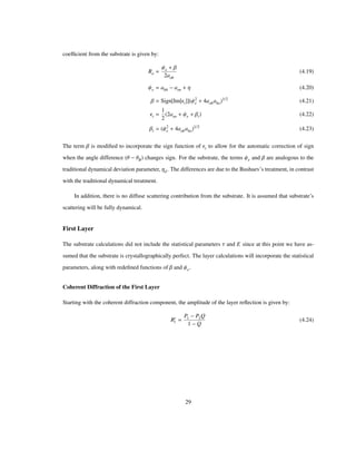
![between these two separate components are controlled by two factors, static Debye-Waller factor (E), and
complex correlation length, Τ.
Following the SDDT treatment developed by Bushuev, the Takagi-Taupin numeric solution to dynamical
diffracting systems can be modified to incorporate defect scattering by decreasing the coupling between X-ray
wavefields (incident plus a single diffracted wavefields). The T-T equations (using Bushuev’s conventions)
can be written as
dEo
dz
iaooEo iaohΦEh (4.1)
dEh
dz
i ahh Η Eh iahoΦ Eo (4.2)
where Eo and Eh are the incident and diffracted amplitudes, Φ exp iH u is the lattice phase factor [5,82]
where H is reflection vector, u is the displacement from the expected lattice points, and Η is the Bushuev
simplified deviation parameter,
Η
k Θ ΘB sin 2ΘB
Γh
(4.3)
where k is the wavevector and Γh is the direction cosine of the diffracted beam. We also invoke the variables
aoo
kΧo
2Γo
:modulates the amplitude Eo entering into the sample (4.4)
ahh
kΧo
2Γh
:modulates the amplitude Eh exiting the sample (4.5)
aoh
kCΧh
2Γo
:modulates forward diffracting amplitude Eh (4.6)
aho
kCΧh
2Γh
:modulates back diffracting amplitude Eo (4.7)
Bushuev followed the general guidelines proposed by Kato [86,87] for the implementation of the statis-
tical theory. The specific procedure of statistical averaging are explained in detail by Bushuev [6,64] and are
also discussed elsewhere [5,88–93,95–97]. The statistically-modified T-T equations can then be written as:
dEc
o
dz
i aoo i aohaho 1 E2
Τ Ec
o iaohEEc
h (4.8)
dE
c
h
dz
i ahh Η i aohaho 1 E2
Τ Ec
h iahoEEc
o (4.9)
The complex correlation length (Τ) will be discussed in the following sections. The addition of c super-
scripts to amplitudes Ec
o and E
c
h indicate that they are coherent (i.e. dynamic) amplitudes. It can be seen that
26](https://image.slidesharecdn.com/2af25ca4-a567-429d-a0c9-5d02c7cc9e50-170206043027/85/20120112-Dissertation7-2-36-320.jpg)
![the coupling between the incident and diffracted beam amplitudes in these equations is mediated by the static
Debye-waller factor (E).
The general solutions to Equations (4.8) and (4.9) are given by
Ec
o Ao1eiΕ1z
Ao2eiΕ2z
(4.10)
Ec
h Ah1eiΕ1z
Ah2eiΕ2z
(4.11)
where the terms Aij are unknown coefficients that will be resolved by using boundary conditions. The Εj
terms are phase functions of the amplitude wave solution. The z represents top of the given layer when z 0,
and bottom of layer when z t where t is thickness of the layer.
Continuing to follow the Bushuev treatment [6, 64], the incoherent (non-dynamic, i.e. kinematic or
diffuse) intensity is described by the energy-transfer equations [82],
dIi
o
dz
ΜoIi
o ΣohIc
h (4.12)
dI
i
h
dz
ΜhIi
h ΣhoIc
o (4.13)
where superscripts i, c represent the incoherent and coherent components, respectively; Ic
o is coherent inten-
sity in the incident direction, while I
c
h is the coherent intensity in diffracted direction, Ii
o is the incoherent
intensity in incident direction, and I
i
h is the incoherent intensity in diffracted direction. The term Μi is the
usual photoelectric absorption divided by the direction cosine (Γi). Note that the treatment of the incoherent
kinematic scattering involves contributions to the intensity, which is in contrast with the development of the
fundamental equations for dynamic scattering which is expressed in terms of amplitudes.
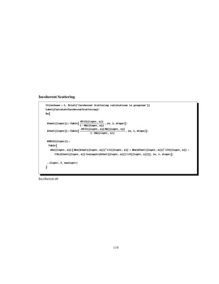
The kinematic cross section term Σij 2 aij
2
1 E2
Τr represents the probability for diffuse scattering,
with the static Debye-Waller factor providing an integral component of the diffuse scattering probability. The
incoherent intensity will be zero if the average displacement of the lattice equals zero (i.e., perfect crystal
or full dynamical scattering). The energy-transfer equations and its adaptations for SDDT application are
discussed in depth by several papers by Kato during the initial development of SDDT theory [82–87].
The total intensity can then be obtained from the two components [6]
It Θ Ic
h Ii
h (4.14)
where I
c
h E
c
h
2
.
27](https://image.slidesharecdn.com/2af25ca4-a567-429d-a0c9-5d02c7cc9e50-170206043027/85/20120112-Dissertation7-2-37-320.jpg)
![4.3 Implementation Method
As mentioned above, the present implementation of the SDDT is based primarily on the approach given by
Bushuev [6], modified with the multilayer model developed by Punegov [91,93]. The coherent (dynamical)
reflection calculations begins at substrate. The layer contributions are calculated iteratively to the total dy-
namical diffraction. The coherent amplitudes calculated for each layer is also used to calculate the incoherent
(diffuse) scattering. The transmission coefficients of the incoherent scattering begins at top-most layer, and
then recursively calculated downward to the substrate. All calculations for coherent and incoherent scattering
for each layer are done first, then the transmission coefficients are calculated separately due to the different
method of recursion (top-down and bottom-up). Once these calculations are completed, the total intensity
can be obtained.
Strain
We assume that the diffracting crystal may be strained as function of depth. Each layer has its own lattice
parameter,
as sao (4.15)
s 1
d
d
(4.16)
where as represents strained lattice parameter expressed in terms of the unstrained lattice parameter, ao. The
term s is the magnitude of the strain, while the term d/d being negative or positive, depending on whether
the strain is compressive or tensile. The definition used here is different from that used by Bushuev [6] which
only alters the location of the Bragg peak for the given layer using
Θo d/d tan ΘB (4.17)
which then alters Bushuev’s simplified deviation parameter
Η k Θ Θo sin 2ΘB/Γh (4.18)
However, this method will not be used in this study.
Substrate
One of the first steps is to calculate the diffracted amplitude from the substrate using some modifications to
the expression for the amplitude E
c
h given by Bushuev [6] and Punegov [93]. Here, the amplitude reflection
28](https://image.slidesharecdn.com/2af25ca4-a567-429d-a0c9-5d02c7cc9e50-170206043027/85/20120112-Dissertation7-2-38-320.jpg)
![of the incoherent scattering becomes
Ii
h Σho Ao1
2
l11 Ao2
2
l22 2Re Ao1Ao2l12 (4.32)
Σho 2 aho
2
1 E2
Re Τ (4.33)
Ao1
1
1 Q
(4.34)
Ao2
Q
1 Q
(4.35)
l11
1 e Μh Μ11 t
Μ11 Μh
(4.36)
l22
1 e Μh Μ22 t
Μ22 Μh
(4.37)
l12
1 e Μh Μ12 t
Μ12 Μh
(4.38)
Μ11 i Ε1 Ε1 (4.39)
Μ22 i Ε2 Ε2 (4.40)
Μ12 i Ε1 Ε2 (4.41)
l11, l22, l12 are the effective thicknesses of the diffuse scattering generation based on which Aoj terms are
used. Basically, it is a physical thickness modulated by absorption and scattering factors. If the given layer
is thin enough (much less than the extinction length), then the effective thickness is approximately equal to
actual thickness (lij t). The term Μij represents the phase difference between Εi and Εj, and the Μh is the
photoelectric absorption with cosine direction (Μ/Γh).
Total Intensity of the First Layer
For the single layer model, determining the total diffracted intensity is straightforward since only incoherent
scattering occurs in one layer. The total intensity of single-layer material in the symmetrical Bragg diffraction
It
Ii
h Rc
l Rc
l (4.42)
With these solutions in place, the simulations of the SDDT became possible. One of the early publi-
cations on SDDT (Bushuev [6]) was successfully duplicated (See Figure 4.1). For this type of replication,
it must be noted that this particular graph is not logarithmic. Typically, for the most part of the disserta-
tion, the intensity is logarithmic. For exceptional cases like this, it will be specifically mentioned that it is
non-logarithmic.
31](https://image.slidesharecdn.com/2af25ca4-a567-429d-a0c9-5d02c7cc9e50-170206043027/85/20120112-Dissertation7-2-41-320.jpg)
![Figure 4.1: Replication of Bushuev’s work [6]
However for the multi-layer model, it will be necessary to incorporate each layer contribution to the
incoherent scattering. In addition, absorption of each layer must be considered. As result, transmission
coefficients will be incorporated into the multilayer model.
Multi-layer Model
For the coherent diffraction of the multi-layer, the only modification from the first layer model is the definition
of Ro to R
c
l 1 where l represents the nth
layer from bottom up starting zero at substrate. All structural variables
are calculated for the given layer, except for the R
c
l 1 which is reflection from layer below or the substrate.
As result, only the variable Q is modified,
Q
P1 R
c
l 1
P2 Rc
l 1
ei Ε1 Ε2 t
(4.43)
which also effects the amplitude of the coherent scattering Ao1, Ao2 used in the incoherent scattering calcula-
tions.
The major addition of the multi-layer model is the amplitude transmission coefficient. The single-layer
model neglected the amplitude transmission coefficient for the incoherent scattering because the substrate
32](https://image.slidesharecdn.com/2af25ca4-a567-429d-a0c9-5d02c7cc9e50-170206043027/85/20120112-Dissertation7-2-42-320.jpg)
![does not have any incoherent scattering. When the multi-layer model is developed, it is necessary to incor-
porate the scattering contribution and absorption from each layer.
The transmission beam is calculated from topmost layer downward to the substrate. Using the results
of [93], we have
l 1, L (L is the topmost layer) (4.44)
T l 1
T l eiΕ
l
1 t l
Q l
eiΕ
l
2 t l
1 Q l
(4.45)
T L
1 (4.46)
In Punegov’s work [93], the Aij terms have the transmission coefficients incorporated into them. However,
for this study,they are not incorporated since the coherent scattering equation does not need the transmission
coefficients due to the terms canceling each other in recursive equation. The topmost layer with the T L
term
has a value of unity since the incident beam profile on the surface of the sample is assumed to be unity. For
more simple programming logistics, this approach is used with the same results. The incoherent scattering
equations will have the transmission coefficients included in the total intensity calculation. The total intensity
for the multi-layers is calculated as:
It
h Rc
LRc
L
L
l 1
T l 2
I
i l
h (4.47)
Complex Correlation Length
The complex correlation length parameter presents a number of difficulties regarding the accurately modeling
of various types of defects. For instance, a defect model of consisting of randomly distributed amorphous
spherical clusters with radius r in which there are no elastic fields outside of the cluster has been presented
in prior treatments [6]. In this case, the real and imaginary components of Τ can be given by [6]
Τ Τr iΤi (4.48)
Τr
6r
x4
1
2
x2
1 cos x x sin x (4.49)
Τi
r
x4
x3
1 cos x 6 x cos x sin x (4.50)
x 2ΨrΓo (4.51)
33](https://image.slidesharecdn.com/2af25ca4-a567-429d-a0c9-5d02c7cc9e50-170206043027/85/20120112-Dissertation7-2-43-320.jpg)
![The spherical cluster model allows the correlation function to be expressed in closed mathematical form,
but it does not represent a realistic model for the typical defects present in semiconductor heterostructures.
The mosaic block model, based on Bushuev [64] would be a more useful model. In this case, only the real
part of Τ is used:
Τr
t
2Ξo
s Θ (4.52)
s Θ
1
exp Π Θ/ 2
(4.53)
2
M
2
o (4.54)
Ξo 2 sin ΘBt/Λ (4.55)
o 1/Ξo (4.56)
where o is width of the reflection of the individual blocks, M is width of the angular distribution of the
mosaic blocks (assumed to be Gaussian), and s represents the convolution of the individual mosaic block
diffraction and the angular distribution of the blocks.
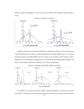
For more better illustration, please refer to Figure 4.2. The function W Α represents the distrubtion of
the mosaic blocks, and M is the width of that function. The Α represents the angular deviation of blocks
from the crystalline surface or the expected angular orientation.
Figure 4.2: Illustration of Mosaic model
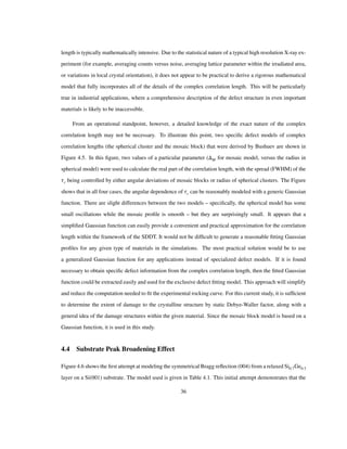
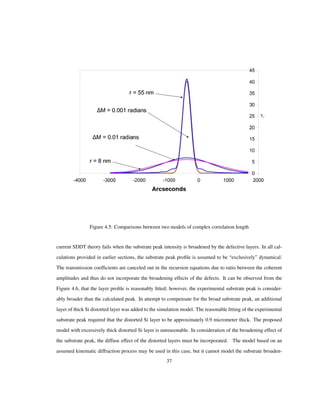
The effect of the correlation length parameter ( M) is illustrated (Figure 4.3) here based on the recent
34](https://image.slidesharecdn.com/2af25ca4-a567-429d-a0c9-5d02c7cc9e50-170206043027/85/20120112-Dissertation7-2-44-320.jpg)
![Figure 4.8: An illustrated example of full range from coherent to incoherent diffraction of the model with all
other parameters fixed
computation times. The lamellar model, which is based on [93], was implemented successfully using the
Bushuev’s model [6,64] (also with modified strain model), allowing for each layer to have its own parameters
for thickness, strain, static Debye-Waller factor, and complex correlation length parameters. In addition, the
broadening effect of substrate peak was implemented to account for diffuse effects of defects on the substrate
peak. The broadening effect implementation allows for more accurate fitting of the experimental rocking
curves, and accounts for the difference between conventional SDDT and the experimental data.
41](https://image.slidesharecdn.com/2af25ca4-a567-429d-a0c9-5d02c7cc9e50-170206043027/85/20120112-Dissertation7-2-51-320.jpg)
![Chapter 5
Modified Statistical Dynamical Diffraction Theory
In this chapter, one of the new parameters that has been proposed in this research, the broadening effect, is
explored . The initial development proposed in previous publication [94] was based on weighted approach
of using each epi-layers of the material’s parameters, and weight them all based on thickness of each layer
weighted against the total thickness of all layers. Unfortunately, that provided to be impractical since the
variables used in the calculations became interchangeable among the layers, making the proper analysis
nearly impossible. As result, a new approach, a layered broadening effect, is proposed and compared against
the weighted broadening effect. Before the comparisons can be made, a section on weighted broadening
effect is necessary for a more clear illustrations of relationship between layer’s defects and its effects on the
substrate peak broadening.
5.1 Weighted Broadening Effect
The parameter Be is represented by weighted static Debye-Waller (Ew), and weighted complex correlation
length (Τw),
Be 1 As 1 Ew Τw (5.1)
where the As is a normalization parameter in respect to the substrate peak. The broadening effect parameter is
controlled by the complex correlation length and the static Debye Waller factor of overall structure to model
the full range from full dynamical (almost no broadening effect) to near-kinematical limit (full broadening
effect). The weighting is based on the overall thickness (tT ) of each given layer thickness (tn),
tT
n
tn (5.2)
Pn
tn
tT
(5.3)
Each layer will have its own values for the Debye Waller factor (E) and the complex correlation length
parameter ( M) which is multiplied by weighted percentage Pn then added together to create a weighted
parameters for the broadening effect.
42](https://image.slidesharecdn.com/2af25ca4-a567-429d-a0c9-5d02c7cc9e50-170206043027/85/20120112-Dissertation7-2-52-320.jpg)
![Figure 5.1: SRIM simulations of ion-implantation: Boron and Germanium respectively.
The range of these given samples allows for additional verifications of the statistical theory’s capabilities
of handling various ranges of the defect development due to different processing elements. The ion-implanted
SiGe samples that has range of annealing temperatures and two different ion species (Germanium for pre-
implantation, and Boron for implantation) provides to be excellent starting point for initial analysis of the
mSDDT capabilities as it has wide range of strained to relaxed profiles of the material.
SiGe Samples
Layers of Si70Ge30 of approximately 50 nm were grown on (001) Si using UHVCVD (Ultra-High Vacuum
Chemical Vapor Deposition), and implanted with either just boron (500eV, 1 1015
cm2
) only or also pre-
implanted with germanium (20keV, 5 1014
cm2
). Along with various annealing conditions, there are two sets
of four samples generated. The following Table 5.1 illustrates various processes involved in these sets.
Table 5.1: Processing of the SiGe sample sets
Implantation As Implanted Annealed at 950 C Annealed at 1100 C Annealed at 1175 C
Boron Only Sample B:1 Sample B:2 Sample B:3 Sample B:4
B and Ge Sample BGe:1 Sample BGe:2 Sample BGe:3 Sample BGe:4
The calculation of ion-implantation depth was performed by SRIM (The Stopping and Range of Ions
in Matter) [98]. The expected depths of the ion profile is estimated at 12.5nm deep for Boron species and
47.5nm for Ge species (Figure 5.1).
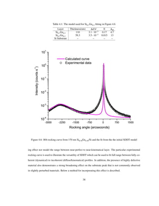
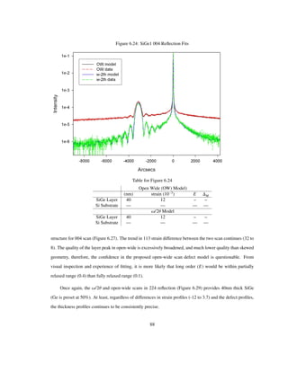
43](https://image.slidesharecdn.com/2af25ca4-a567-429d-a0c9-5d02c7cc9e50-170206043027/85/20120112-Dissertation7-2-53-320.jpg)
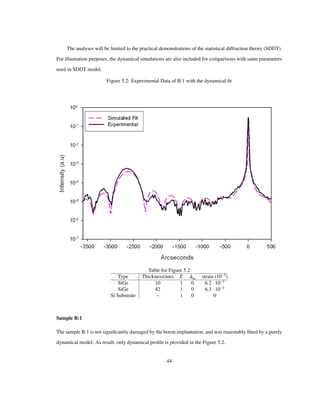
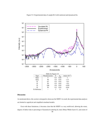
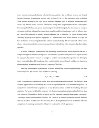
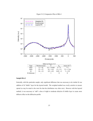
![Figure 5.6: Experimental data of sample BGe:1 with statistical and dynamical fits.
Table for Figure 5.6
Type Thickness(nm) E m strain 10 3
SiGe 6 0.1 0 7.7
SiGe 35 0.1 0 7.5
Si 10 0.5 0.05 3
Si Substrate – 1 0 0
the defects (based on correlation length function Τ) to be approximately fitted in a lamellar fashion to extract
the overall structure of the sample.
As proposed in the published article [94], the focus is on generalized parameters of static Debye-Waller
factor as in degrees of dynamical scattering, and generic Gaussian distribution for the correlation length
function allows for non-specific defect structures to be fitted in the test models. The mosaic model based on
Bushuev [64] was used as a “generic” Gaussian model since it had Gaussian function as part of the mosaic
distribution.
49](https://image.slidesharecdn.com/2af25ca4-a567-429d-a0c9-5d02c7cc9e50-170206043027/85/20120112-Dissertation7-2-59-320.jpg)
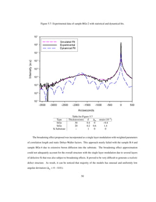
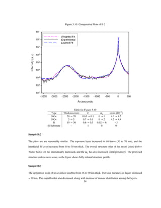
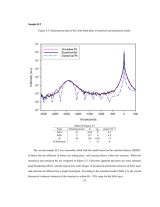
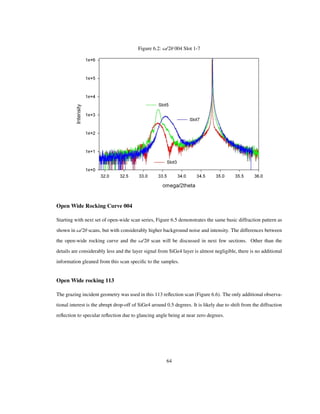
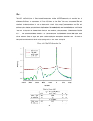
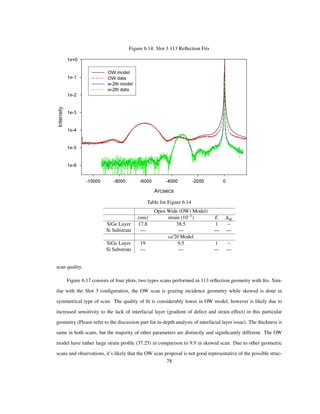
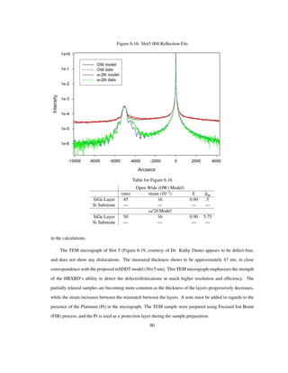
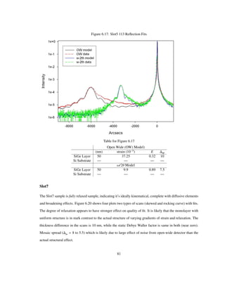
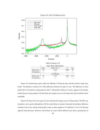
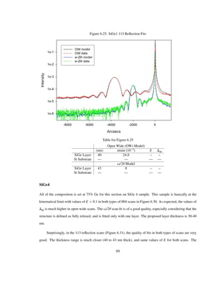
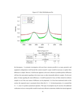
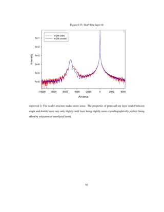
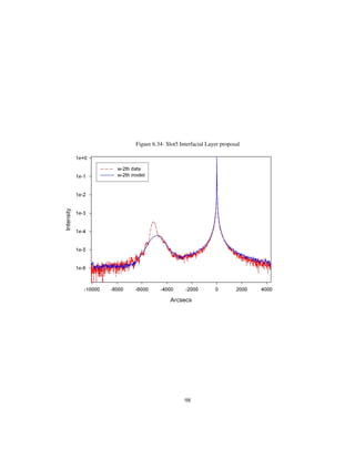
![broad diffraction profile of layer. The Slot7 sample is actually similar to SiGe3, but is slightly more strained.
Figure 6.1: Ω/2Θ 004 SiGe1-4
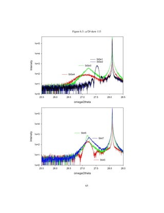
Ω/2Θ skew 113
The sample was rotated until the 113 vector is in line with the detector rotational plane, allowing for
symmetrical-like scan to be performed. All of the observations stated in earlier section is similar here in
Figure 6.3
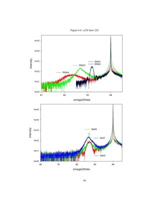
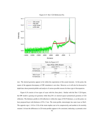
Ω/2Θ skew 224
In same respect to the skew 113 reflection, the sample is rotated until the [224] vector coincides with the
detector’s rotation plane to allow for symmetrical-like scan. Other than similar observations previously stated,
there is interesting trend that is sharply contrasted in these two distinct sets of samples. In SiGe series,
the composition of Germanium varies, hence the peak locations of the SiGe layer also vary approximately.
As in the Slot series, the composition remains at 50%, the location of layer peak of all samples remains
approximately at the same Bragg’s angle. Please refer to Figure 6.4.
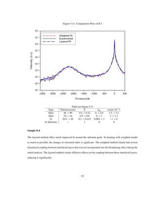
63](https://image.slidesharecdn.com/2af25ca4-a567-429d-a0c9-5d02c7cc9e50-170206043027/85/20120112-Dissertation7-2-73-320.jpg)
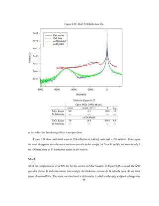
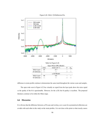
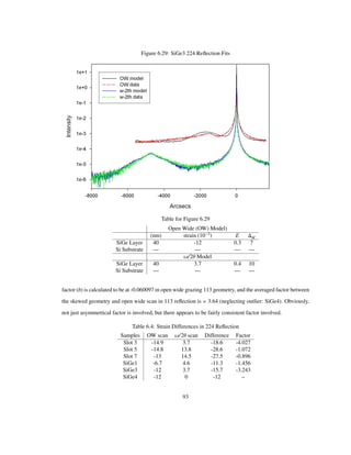
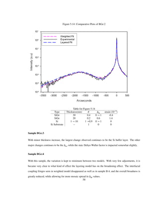
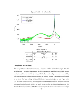
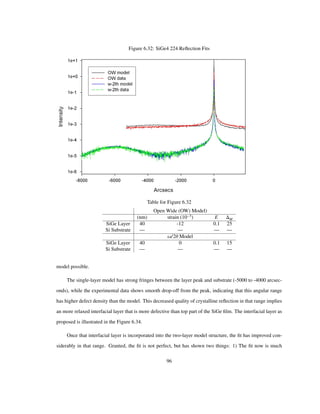
![Figure 6.30: SiGe4 004 Reflection Fits
Table for Figure 6.30
Open Wide (OW) Model)
(nm) strain 10 3
E M
SiGe Layer 30 0 0.1 20
Si Substrate — — — —
Ω/2Θ Model
SiGe Layer 40 5.5 0.1 9
Si Substrate — — — —
Table 6.4 lists the strain profiles for all samples in the 224 reflection. The asymmetrical factor (b) is
calculated to be at -6.4869 for the open wide grazing geometry. The differences between the skewed and the
grazing geometry in the 224 reflection does not offer consistent values or factor other than that the strain is
in opposite directions (compressively vs. tensilely).
In addition, it has been apparent in the comparisons of different software that the asymmetrical reflec-
tions, strain vs relaxation definitions, and also the existence of varying definition of fringes crops from many
different types of assumptions made within the matrix of calculations. For instance the deviation parameter
proposed in this dissertation is not the exactly correct one. For a good introduction of this subject, please
refer to the work of Zaus [99].
94](https://image.slidesharecdn.com/2af25ca4-a567-429d-a0c9-5d02c7cc9e50-170206043027/85/20120112-Dissertation7-2-104-320.jpg)
![Appendix A
Equivalence of Bushuev’s Treatment of T-T equations to
well-known dynamical T-T equations based on Bartels,
Hornstra and Lobeek’s work
This Appendix is provided for reference and comparison between two distinctly different methods of T-T
equation implementation. The derivation is only provided to demonstrate the equality between these two
approaches.
Starting with equation 2 in [6]:
dEo
dz
i aoo ispΤ Eo iaohEEh (A.1)
dEh
dz
i ahh Η ipΤ Eh iahoEEo (A.2)
where we will use these given definitions (repeated here for quick reference)
Ψ ahh aoo Η (A.3)
p aohaho 1 E2
(A.4)
agg ΚCΧgg /2Γg (A.5)
Η Κ Θ Θo sin 2ΘB/Γh (A.6)
Κ 2Π/Λ (A.7)
Since the article focus exclusively on Braggs reflection, s 1, and with Αh 2 Θ Θo sin 2ΘB for
convenience,
dEo
dz
i
ΠΧoo
ΛΓo
i
CΠΧoh
ΛΓo
CΠΧho
ΛΓh
1 E2
Τ Eo
iCΠΧoh
ΛΓo
EEh (A.8)
106](https://image.slidesharecdn.com/2af25ca4-a567-429d-a0c9-5d02c7cc9e50-170206043027/85/20120112-Dissertation7-2-116-320.jpg)
![dEh
dz
i
ΠΧhh ΠΑh
ΛΓh
i
CΠΧoh
ΛΓo
CΠΧho
ΛΓh
1 E2
Τ Eh
iCΠΧho
ΛΓh
EEo (A.9)
Let
Eh
Eo
R where R represents a ratio between incident and reflected amplitude and using Quotient Rule
dR
dz
d
dz
Eh
Eo
Eo
dEh
dz Eh
dEo
dz
E2
o
(A.10)
(A.11)
the completed solution of ampitude ratio version of Bushuev is presented.
Λ
CΠi
dR
dz
Χoh
Γo
ER2
Χhh
CΓh
Χoo
CΓo
Αh
CΓh
i
Χoh
Γo
CΠΧho
ΛΓh
1 E2
Τ Τ R
Χho
Γh
E
(A.12)
Now, the ampitude ratio treatment in [65] use “rationalized” amplitude ratio: X
ΧH
ΧH
ΓH
Γo
EH
Eo
In addition,
for convention comparsion let Χhh Χoo Χo, Χoh Χ h, and Χho Χh. Also, in this study, Τ Τ ,
ΓoΓH
ΧHΧH
Λ
CΠi
dX
dz
EX2
1
ΧHΧH
b 1 Χo
bC
bΑh
bC
i
Χoh
ΓoΓH
CΠΧho
Λ
1 E2
2Τ X
E
(A.13)
Let 1/Q
ΓoΓh
ΧH ΧH
Λ
CΠi .
dX
dz
QEX2
Q
1
ΧHΧH
b 1 Χo
bC
bΑh
bC
i
Χoh
ΓoΓH
CΠΧho
Λ
1 E2
2Τ X
QE
(A.14)
107](https://image.slidesharecdn.com/2af25ca4-a567-429d-a0c9-5d02c7cc9e50-170206043027/85/20120112-Dissertation7-2-117-320.jpg)
![In dynamical limit, the complex correlation length will be zero, Τ 0 and the static Debye-Waller will
equal unity (E 1). As result,
dX
dz
QX2
Q
1
ΧHΧH
b 1 Χo
bC
bΑh
bC
X
Q
(A.15)
Using the standard dynamical devitation parameter (denoting subscript d for clairfication)
Ηd
1
2 1 b Χo b Θ ΘB sin 2ΘB
bC ΧHΧH
(A.16)
Let T iQz,
i
dX
dT
X2
2ΗdX 1 (A.17)
the resultant equation are the same as the equation 1 presented in [65]
108](https://image.slidesharecdn.com/2af25ca4-a567-429d-a0c9-5d02c7cc9e50-170206043027/85/20120112-Dissertation7-2-118-320.jpg)
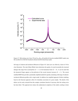
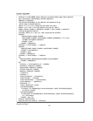
![use fitting procedure which calls Genetic Algorithm into action. The Genetic Algorithm is based on the
article by Wormington et al [100]with some minor modifications. This module repetitively calls up on the
Central Algorithm to generate each iteration of possible model fit for each population of the parameters to be
evaluated. Once the cycle is completed, the result is then forwarded to Graph Generator to be plotted back
into the Main Interface. However, this diagram only illustrates the first layer of the logistics involved. The
Central Algorithm, by itself, is also yet another set of packages in a specific process.
Central Algorithm
Transmission Incoherent Scattering
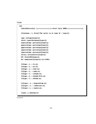
Cycler
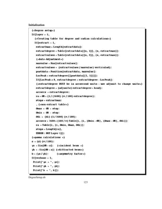
Initialization
SubstrateLayers
Material Database
Broadening
The Initialization, if fitting procedure is involved, will analyze and extract the experimental data’s points,
resolution, substrate peak location, etc and perform additional basic conversion process for transition between
graph data to mathematical matrix. Once that is completed, the Substrate is called to calculate the substrate
diffraction profile, since the mathematical operations between layers and substrate is significantly different.
For additional explanations, please refer to the article [94]. As the Cycler iterate from substrate toward
top-most layer, calling upon Layers for subsequent layer calculations, while updating the current material
parameters by accessing Material Database. Each time a layer is calculated, broadening effect is also calcu-
lated (Broadening). When the cycling is completed, the data is then forwarded back into Central Algorithm
which then use Transmission (to calculate transmission coefficients), and Incoherent Scattering (to calculate
the diffuse scattering).
110](https://image.slidesharecdn.com/2af25ca4-a567-429d-a0c9-5d02c7cc9e50-170206043027/85/20120112-Dissertation7-2-120-320.jpg)
![B.2 Capabilities
This section discusses some of the program’s properties.
The following reflections has been implemented (it’s quite easy to add more if necessary),
• [004]
• [111]
• [224]
• [113]
• [002]
• [022]
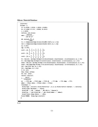
and all are available in grazing exit, grazing incidence, or symmertical geometry. The material database
that has been developed contains seven different types of materials:
1. Si
2. Ge
3. SixGe1 x
4. GaAs
5. GeGaAs (Diamond structure)
6. Ge-GaAs (hybrid of Diamond/Zincblende structure)
7. AlGaAs (Zincblende structure)
The background noise fitting can be done several ways. First one is basic “flatline” addition of base
noise which can be used in complementary form with second function of square root of the intensity. The
third method is recommended. The data set sampling of control sample is used as a background. The only
pitfall of the third approach is the unnatural enhancement of intensity near and around the diffraction peaks.
It is possible to modify the control sample data sets to reduce that effect based on logarithmic approach.
In fitting algorithm, four parameters are automatically included (thickness, strain, m, and E). The
composition is not included since the strain will compound that parameter since they both have same effect
on the diffraction profile. A selection of diffraction profile can be done by setting a range of the angle for
the best-fit focus instead of using entire scan. For adjustment, horizontal and vertical adjustments are also
manually done.
111](https://image.slidesharecdn.com/2af25ca4-a567-429d-a0c9-5d02c7cc9e50-170206043027/85/20120112-Dissertation7-2-121-320.jpg)
![Bibliography
[1] http://www.crct.polymtl.ca/fact/documentation/BINARY/Ge-Si.jpg.
[2] D. J. Paul, Semiconductor Science and Technology 19(10), R75 (2004).
[3] http://www.sp.phy.cam.ac.uk/ SiGe/Misfit.html.
[4] J. Lindner, App. Phys. A 77, 27–38 (2003).
[5] A. Authier, Dynamical Theory of X-Ray Diffraction, revised edition, IUCr Monographs on Crystal-
lography, Vol. 11 (Oxford University Press, 2001).
[6] V. A. Bushuev, Sov. Phys. Solid State 31(11), 1877–1882 (1989).
[7] M. Wautelet, European Journal of Physics 22(6), 601 (2001).
[8] J. B. Johnson, X. LIU, B. A. Orner, and R. M. Rassel, Schottky barrier diodes for millimeter wave
sige bicmos applications, 06 2011.
[9] M. H. Yu, L. T. Wang, T. C. Huang, T. L. Lee, and H. C. Cheng, Journal of The Electrochemical
Society 159(3), H243–H249 (2012).
[10] M. Kolahdouz, L. Maresca, R. Ghandi, A. Khatibi, and H. H. Radamson, Journal of The Electro-
chemical Society 158(4), H457–H464 (2011).
[11] A. Fox, B. Heinemann, R. Barth, S. Marschmeyer, C. Wipf, and Y. Yamamoto, Sige:c hbt architecture
with epitaxial external base, in: Bipolar/BiCMOS Circuits and Technology Meeting (BCTM), 2011
IEEE, (oct. 2011), pp. 70 –73.
[12] H. Trinkaus, D. Buca, R. A. Minamisawa, B. Holländer, M. Luysberg, and S. Mantl, Journal of
Applied Physics 111(1), 014904 (2012).
[13] J. Suh, R. Nakane, N. Taoka, M. Takenaka, and S. Takagi, Applied Physics Letters 99(14), 142108
(2011).
[14] T. Y. Lin, H. C. Wen, Z. C. Chang, W. K. Hsu, C. P. Chou, C. H. Tsai, and D. Lian, Journal of Physics
and Chemistry of Solids 72(6), 789 – 793 (2011).
134](https://image.slidesharecdn.com/2af25ca4-a567-429d-a0c9-5d02c7cc9e50-170206043027/85/20120112-Dissertation7-2-144-320.jpg)
![[15] Z. Xue, X. Wei, B. Zhang, A. Wu, M. Zhang, and X. Wang, Applied Surface Science 257(11), 5021
– 5024 (2011).
[16] A. R. Denton and N. W. Ashcroft, Phys. Rev. A 43(Mar), 3161–3164 (1991).
[17] J. Matthews and A. Blakeslee, Journal of Crystal Growth 27(0), 118 – 125 (1974).
[18] J. Matthews and A. Blakeslee, Journal of Crystal Growth 29(3), 273 – 280 (1975).
[19] J. Matthews and A. Blakeslee, Journal of Crystal Growth 32(2), 265 – 273 (1976).
[20] K. Ang, K. Chui, V. Bliznetsov, C. Tung, A. Du, N. Balasubramanian, G. Samudra, M. F. Li, and
Y. Yeo, App. Phys. Lett. 86 (2005).
[21] H. Itokawa, N. Yasutake, N. Kusunoki, S. Okamoto, N. Aoki, and I. Mizushima, App. Surface
Science 254, 6135–6139 (2008).
[22] C. Calmes, D. Bouchier, D. Débarre, and C. Clerc, App. Phys. Lett. 81(15), 2746–2748 (2002).
[23] S. T. Chang, C. Y. Lin, and S. H. Liao, App. Surface Science 254, 6203–6207 (2008).
[24] C. Förster, V. Cimalla, K. Brückner, M. Hein, J. Pezoldt, and O. Ambacher, Mat. Sc. Eng. C 25,
804–808 (2005).
[25] J. W. H. et al, IEEE Transcations on Electron Devices 56(4), 641–647 (2009).
[26] J. M. Hartmann, T. Ernst, V. Loup, F. Ducroquet, G. Rolland, D. Lafond, P. Holliger, F. Laugier,
M. N. Séméria, and S. Deleonibus, J. App. Phys. 92(5), 2368–2373 (2002).
[27] J. M. Hartmann, T. Ernst, F. Ducroquet, G. Rolland, D. Lafond, A. M. Papon, R. Truche, P. Holliger,
F. Laugier, M. N. Séméria, and S. Deleonibus, Semicond. Sci. Technol. 19, 593–601 (2004).
[28] C. Guedj, G. Calvarin, and B. Piriou, J. Appl. Phys. 83(8), 4064–4068 (1998).
[29] K. M. Kramer and M. O. Thompson, J. Appl. Phys. 79(8), 4118–4123 (1996).
[30] K. Eberl, K. Brunner, and W. Winter, Thin Solid Films 294, 98–104 (1997).
[31] S. Pantelides and S. Zollner, Silicon-germanium carbon alloy, Optoelectronic properties of semicon-
ductors and superlattices (Taylor & Francis, 2002).
135](https://image.slidesharecdn.com/2af25ca4-a567-429d-a0c9-5d02c7cc9e50-170206043027/85/20120112-Dissertation7-2-145-320.jpg)
![[32] R. F. Davis, G. Kelner, M. Shur, J. W. Palmour, and J. A. Edmond, Thin film deposition and micro-
electronic and optoelectronic device fabrication and characterization in monocrystalline alpha and
beta silicon carbide, in: Proceedings of the IEEE, (1991), pp. 677–701.
[33] C. W. Liu and J. C. Sturm, J. Appl. Phys. 82(9), 4558–4565 (1997).
[34] I. Golecki, F. Reidinger, and J. Marti, Appl. Phys. Lett. 60(14), 1703–1705 (1992).
[35] M. Berti, D. D. Salvador, A. V. Drigo, F. Romanato, J. Stangl, S. Zerlauth, F. Schäffler, and G. Bauer,
Appl. Phys. Letters 72(13), 1602–1604 (1998).
[36] Z. Kovats, T. H. Metzger, J. Peisl, J. Stangl, M. Mühlberger, Y. Zhuang, F. Schäffler, and G. Bauer,
Appl. Phys. Letters 76(23), 3409–3411 (2000).
[37] A. Fissel, J. Cryst. Growth 227-228, 805–810 (2001).
[38] J. W. Strane, H. J. Stein, S. R. Lee, S. T. Picraux, J. K. Watanabe, and J. W. Mayer, J. Appl. Phys.
76(6), 3656–3668 (1994).
[39] G. Ambrosone, D. K. Basa, U. Coscia, E. Tresso, A. Chiodoni, E. Celasco, N. Pinto, and R. Murri,
phys. status. solidi c 7(3-4), 770–773 (2010).
[40] U. Coscia, G. Ambrosone, D. K. Basa, E. Tresso, A. Chiodoni, N. Pinto, and R. Murri, App. Phys. A
(2010).
[41] U. Coscia, G. Ambrosone, S. Lettieri, P. Maddalena, P. Rava, and C. Minarini, Thin Solid Films 427,
284–288 (2003).
[42] U. Coscia, G. Ambrosone, D. K. Basa, S. Ferrero, P. D. Veneri, L. V. Mercaldo, I. Usatii, and
M. Tucci, Phys. Status Solidi C 7(3-4), 766–769 (2010).
[43] D. K. Basa, G. Ambrosone, U. Coscia, and A. Setaro, App. Surface Science 255, 5528–5531 (2009).
[44] G. B. Tong, S. M. A. Gani, M. R. Muhamad, and S. A. Rahman, High temperature post-deposition
annealing studies of layer-by-layer(lbl) deposited hydrogenated amorphous silicon films, in: Mater.
Res. Soc. Symp. Proc. Vol. 1153, (2009).
[45] G. Ambrosone, D. K. Basa, U. Coscia, and M. Fathallah, J. Appl. Phys. 104, 123520 (2008).
136](https://image.slidesharecdn.com/2af25ca4-a567-429d-a0c9-5d02c7cc9e50-170206043027/85/20120112-Dissertation7-2-146-320.jpg)
![[46] G. Ambrosone, D. K. Basa, U. Coscia, L. Santamaria, N. Pinto, M. Ficcadenti, L. Morresi, L. Craglia,
and R. Murri, Engergy Procedia 2, 3–7 (2010).
[47] G. Ambrosone, D. K. Basa, U. Coscia, and P. Rava, Thin Solid Films 518, 5871–5874 (2010).
[48] D. K. Basa, G. Abbate, G. Ambrosone, U. Coscia, and A. Marino, J. Appl. Phys 107, 023502 (2010).
[49] M. Berti, D. D. Salvador, A. Drigo, M. Petrovich, J. Stangl, F. SchÃd’ffler, S. Zerlauth, G. Bauer,
and A. Armigliato, Micron 31(3), 285 – 289 (2000).
[50] B. E. Warren, X-Ray Diffraction (Dover Publications, 1990).
[51] W. H. Zachariasen, Theory of X-Ray Diffaction in Crystals (Dover Publications, Inc., 1945).
[52] D. K. Bowen and B. K. Tanner, High Resolution X-ray Diffractometry and Topography (Tayor &
Francis Inc., 1998).
[53] U. Pietsch, V. Holý, and T. Baumbach, High-Resolution X-Ray Scattering: From Thin Films to
Lateral Nanostructures, second edition (Springer, 2004).
[54] B. Cullity and S. Stock, Elements of x-ray diffraction, Pearson education (Prentice Hall, 2001).
[55] J. Als-Nielsen and D. McMorrow, Elements of modern X-ray physics (Wiley, 2001).
[56] A. J. C. Wilson and E. Prince (eds.), Mathematical, Physical and Chemical Tables, International Ta-
bles For Crystallograhpy, Vol. C (Kluwer Academic Publishers, 1999).
[57] C. Hammond, The basics of crystallography and diffraction, IUCr texts on crystallography (Oxford
University Press, 2001).
[58] T. Siegrist, Journal of Applied Crystallography 30(3), 418–419 (1997).
[59] B. W. Batterman and H. Cole, Rev. Mod. Phys. 36, 681–717 (1964).
[60] J. C. SLATER, Rev. Mod. Phys. 30(Jan), 197–222 (1958).
[61] S. Takagi, Acta Cryst. 15, 1311–2 (1962).
[62] S. Takagi, J. Phys. Soc. Japan 26(5), 1239–1253 (1969).
[63] D. Taupin, Bull. Soc. Fr. Minér. Cryst. 87, 469–511 (1964).
137](https://image.slidesharecdn.com/2af25ca4-a567-429d-a0c9-5d02c7cc9e50-170206043027/85/20120112-Dissertation7-2-147-320.jpg)
![[64] V. A. Bushuev, Sov. Phys. Cryst. 34(2), 163–167 (1989).
[65] W. J. Bartels, J. Hornstra, and D. J. W. Lobeek, Acta Cryst. A42, 539–545 (1986).
[66] http://www.bruker-axs.com/stress.html.
[67] http://www.jvsemi.com/featured-products/featured-products/rads.html.
[68] M. Servidori, F. Cembali, and S. Milita, Characterization of lattice defects in ion-implanted silicon,
in: X-ray and Neutron Dynamical Diffraction: Theory and Applications, edited by A. Authier and
B.K. Tanner, (Plenum Press, 1996), pp. 301–321.
[69] K. D. Shcherbachev, V. T. Bublik, V. N. Mordkovich, and D. M. Pazhin, J. Phys. D 38, A126–131
(2005).
[70] V. S. Speriosu, J. Appl. Phys. 52(10), 6094–6103 (1981).
[71] V. S. Speriosu and T. Vreeland, J. Appl. Phys. 56(6), 1591–1600 (1984).
[72] M. A. Krivoglaz, X-ray and Neutron Diffraction in Nonideal Crystals (Springer, 1996).
[73] E. L. Gartstein, Z. Phys. B 88, 327–332 (1992).
[74] G. Bhagavannarayana and P. Zaumseil, J. Appl. Phys. 82, 1172–1177 (1997).
[75] V. M. Kaganer, R. Kohler, M. Schmidbauer, R. Opitz, and B. Jenichen, Phys. Rev. B 55, 1793–1810
(1997).
[76] V. Holý, A. A. Darhuber, J. Stangl, S. Zerlauth, F. Schaffler, G. Bauer, N. Darowski, D. Lubbert,
U. Pietsch, and I. Vavra, Phys. Rev. B 58, 7934–7943 (1998).
[77] V. B. Molodkin, S. I. Olikhovskii, E. N. Kislovskii, E. G. Len, and E. V. Pervak, Phys. Stat. Sol. (b)
227, 429–447 (2008).
[78] V. B. Molodkin, S. I. Olikhovskii, E. N. Kislovskii, I. M. Fodchuk, E. S. Skakunova, E. V. Pervak, and
V. V. Molodkin, Phys. Stat. Sol. (a) 204, 2606–2612 (2007).
[79] S. I. Olikhovskii, V. B. Molodkin, E. N. Kislovskii, E. G. Len, and E. V. Pervak, Phys. Stat. Sol. (b)
231, 199–212 (2002).
138](https://image.slidesharecdn.com/2af25ca4-a567-429d-a0c9-5d02c7cc9e50-170206043027/85/20120112-Dissertation7-2-148-320.jpg)
![[80] E. N. Kislovskii, S. I. Olikhovskii, V. B. Molodkin, V. V. Nemoshakalenko, V. P. Krivitsy, E. G. Len,
E. V. Pervak, G. E. Ice, and B. C. Larson, Phys. Stat. Sol. (b) 231, 213–221 (2002).
[81] V. B. Molodkin, S. I. Olikhovskii, E. N. Kislovskii, T. P. Vladimirova, and E. S. Skakunova, Phys.
Rev. B 78, 224109 (2008).
[82] N. Kato, Acta Cryst. A32, 453–457 (1976).
[83] N. Kato, Acta Cryst. A32, 458–466 (1976).
[84] N. Kato, Acta Cryst. A35, 9–16 (1979).
[85] N. Kato, Acta Cryst. A36, 171–177 (1980).
[86] N. Kato, Acta Cryst. A36, 763–769 (1980).
[87] N. Kato, Acta Cryst. A36, 770–778 (1980).
[88] V. I. Punegov, Sov. Phys. Tech. Phys. 35(10), 1162–1164 (1990).
[89] V. I. Punegov, Sov. Phys. Cryst. 35(3), 336–340 (1990).
[90] V. I. Punegov, Sov. Phys. Solid State 33(1), 136–140 (1991).
[91] V. I. Punegov, Phys. Stat. Sol. a 136(9), 9–19 (1993).
[92] K. M. Pavlov and V. I. Punegov, Acta Cryst. A56, 227–234 (2000).
[93] V. I. Punegov and A. V. Kharchenko, Cryst. Reports 43(6), 1020–1025 (1998).
[94] P. K. Shreeman and R. J. Matyi, J. Appl. Cryst. 43, 550–559 (2010).
[95] M. Li, Z. Mai, J. Li, C. Li, and S. Cui, Acta Cryst. A51, 350–353 (1995).
[96] H. An, M. Li, S. Yang, Z. Mai, and S. Liu, J. Cryst. Growth 148, 31–34 (1995).
[97] K. M. Pavlov, V. I. Punegov, and N. N. Faleev, JETP 80(6), 1090–1097 (1995).
[98] http://www.srim.org.
[99] R. Zaus, J. Appl. Cryst. 26, 801–811 (1993).
139](https://image.slidesharecdn.com/2af25ca4-a567-429d-a0c9-5d02c7cc9e50-170206043027/85/20120112-Dissertation7-2-149-320.jpg)
![[100] M. Wormington, C. Panaccione, K. M. Matney, and D. K. Bowen, Philosophical Transactions of the
Royal Society of London. Series A: Mathematical, Physical and Engineering Sciences 357(1761),
2827–2848 (1999).
140](https://image.slidesharecdn.com/2af25ca4-a567-429d-a0c9-5d02c7cc9e50-170206043027/85/20120112-Dissertation7-2-150-320.jpg)


![[A. hobbacher] fatigue_design_of_welded_joints_and](https://cdn.slidesharecdn.com/ss_thumbnails/a-160512092007-thumbnail.jpg?width=640&height=640&fit=bounds)