Download to read offline

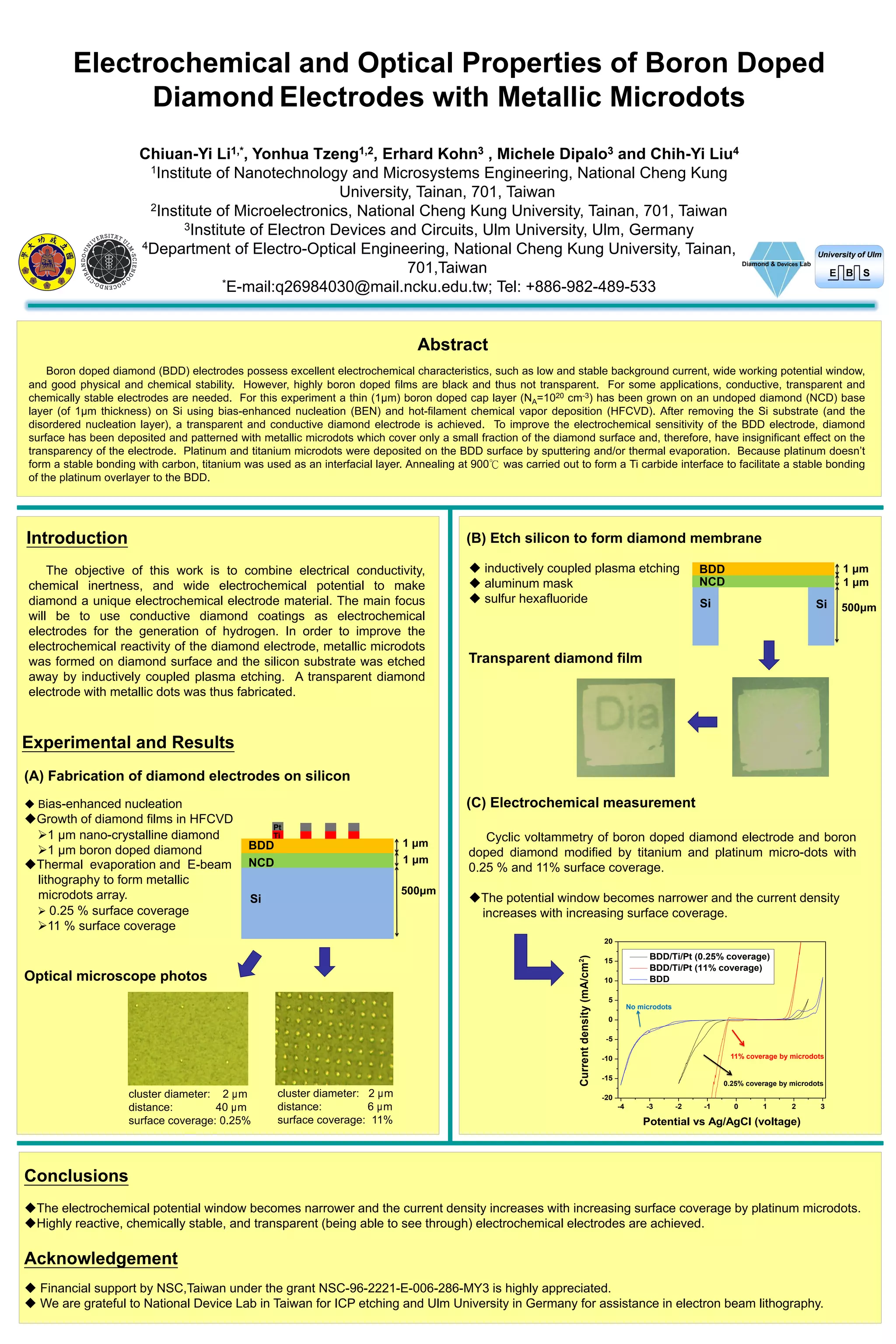

Boron doped diamond films were grown on silicon substrates and patterned with platinum and titanium microdots to create transparent and conductive diamond electrodes. The silicon substrate was then etched away using inductively coupled plasma to form a free-standing diamond membrane. Metallic microdots with surface coverages of 0.25% and 11% were deposited on the diamond surface. Electrochemical measurements showed that the potential window narrowed and current density increased with higher microdot coverage. The diamond electrodes demonstrated high reactivity, chemical stability, and transparency, making them promising for applications requiring these properties.


