
Recommended
More Related Content
What's hot
Similar to Hv9910 led driver
Similar to Hv9910 led driver (20)
Recently uploaded
Recently uploaded (20)
Hv9910 led driver
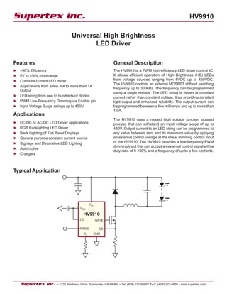
- 1. HV9910 Features >90% Efficiency 8V to 450V input range Constant-current LED driver Applications from a few mA to more than 1A Output LED string from one to hundreds of diodes PWM Low-Frequency Dimming via Enable pin Input Voltage Surge ratings up to 450V Applications DC/DC or AC/DC LED Driver applications RGB Backlighting LED Driver Back Lighting of Flat Panel Displays General purpose constant current source Signage and Decorative LED Lighting Automotive Chargers ► ► ► ► ► ► ► ► ► ► ► ► ► ► General Description The HV9910 is a PWM high-efficiency LED driver control IC. It allows efficient operation of High Brightness (HB) LEDs from voltage sources ranging from 8VDC up to 450VDC. The HV9910 controls an external MOSFET at fixed switching frequency up to 300kHz. The frequency can be programmed using a single resistor. The LED string is driven at constant current rather than constant voltage, thus providing constant light output and enhanced reliability. The output current can be programmed between a few milliamps and up to more than 1.0A. The HV9910 uses a rugged high voltage junction isolated process that can withstand an input voltage surge of up to 450V. Output current to an LED string can be programmed to any value between zero and its maximum value by applying an external control voltage at the linear dimming control input of the HV9910. The HV9910 provides a low-frequency PWM dimming input that can accept an external control signal with a duty ratio of 0-100% and a frequency of up to a few kilohertz. Typical Application Universal High Brightness LED Driver HV9910 VIN GATE PWMD VDD LD CS RT GND
- 2. 2 HV9910 Ordering Information Device Package Options SOIC-16 SOIC-8 HV9910 HV9910NG-G HV9910LG-G -G indicates package is RoHS compliant (‘Green’) Absolute Maximum Ratings Parameter Value VIN to GND -0.5V to +470V CS -0.3V to (VDD + 0.3V) LD, PWM_D to GND -0.3V to (VDD - 0.3V) GATE to GND -0.3V to (VDD + 0.3V) VDDMAX 13.5V Continuous Power Dissipation (TA = +25°C) (Note 1) 16-Pin SO (derate 7.5mW/°C above +25°C) 750mW 8-Pin SO (derate 6.3mW/°C above +25°C) 630mW Operating temperature range -40°C to +85°C Junction temperature +125°C Storage temperature range -65°C to +150°C Symbol Parameter Min Typ Max Units Conditions Electrical Characteristics (Over recommended operating conditions unless otherwise specified - TA = 25°C) Absolute Maximum Ratings are those values beyond which damage to the device may occur. Functional operation under these conditions is not implied. Continuous operation of the device at the absolute rating level may affect device reliability. All voltages are referenced to device ground. VINDC Input DC supply voltage range 8.0 450 V DC input voltage IINsd Shut-down mode supply current - 0.5 1 mA Pin PWM_D to GND, VIN = 8V VDD Internally regulated voltage 7.0 7.5 8.0 V VIN = 8 – 450V, IDD(ext) = 0, pin GATE open VDDmax Maximal pin VDD voltage - - 13.5 V When an external voltage applied to pin VDD IDD(ext) VDD current available for external circuitry 1 - - 1.0 mA VIN = 8 – 100V UVLO VDD undervoltage lockout threshold 6.45 6.7 6.95 V VIN rising ∆UVLO VDD undervoltage lockout hysteresis - 500 - mV VIN falling VEN(lo) Pin PWM_D input low voltage - - 1.0 V VIN = 8 – 450V VEN(hi) Pin PWM_D input high voltage 2.4 - - V VIN = 8 – 450V REN Pin PWM_D pull-down resistance 50 100 150 kΩ VEN = 5V VCS(hi) Current sense pull-in threshold voltage 225 250 275 mV @TA = -40°C to +85°C VGATE(hi) GATE high output voltage VDD -0.3 - VDD V IOUT = 10mA VGATE(lo) GATE low output voltage 0 - 0.3 V IOUT = -10mA fOSC Oscillator frequency 20 80 25 100 30 120 kHz kHz RT = 1.00MΩ RT = 226kΩ DMAXhf Maximum PWM duty cycle - - 100 % FPWMhf = 25kHz, at GATE, CS to GND. VLD Linear dimming pin voltage range 0 - 250 mV @TA = <85°C, VIN = 12V TBLANK Current sense blanking interval 150 215 280 ns VCS = 0.55VLD , VLD = VDD 1 Also limited by package power dissipation limit, whichever is lower. 8-Lead SOIC16-Lead SOIC NC NC NC NCNC NC NC NC VIN CS GND GATE PWM_D VDD LD ROSC PWM_D VDD LD ROSCVIN CS GND GATE Pin Configurations
- 3. 3 HV9910 Block Diagram & Typical Applications Pin SOIC-16 SOIC-8 Description VIN 1 1 Input voltage 8V to 450V DC CS 4 2 Senses LED string current GND 5 3 Device ground GATE 8 4 Drives the gate of the external MOSFET PWM_D 9 5 Low Frequency PWM Dimming pin, also Enable input. Internal 100kΩ pull-down to GND VDD 12 6 Internally regulated supply voltage (7.5V nominal). Can supply up to 1mA for external circuitry. A sufficient storage capacitor is used to provide storage when the rectified AC input is near the zero crossings. LD 13 7 Linear dimming by changing the current limit threshold at current sense comparator RT 14 8 Oscillator control. A resistor connected between this pin and ground sets the PWM frequency. No Connects (NC) are not internally connected and may be used for pass-thru PCB traces. CM CM OSC CS GND RT LD PWM_D S R Q HV9910 VIN VDD VIN VDD 100k 250mV REG 7.5V GATE Pinout Symbol Parameter Min Typ Max Units Conditions tDELAY Delay from CS trip to GATE lo - - 300 ns VIN = 12V, VLD = 0.15, VCS = 0 to 0.22V after TBLANK tRISE GATE output rise time - 30 50 ns CGATE = 500pF tFALL GATE output fall time - 30 50 ns CGATE = 500pF
- 4. 4 HV9910 Application Information AC/DC Off-Line Applications The HV9910 is a low-cost off-line buck or boost converter control IC specifically designed for driving multi-LED stings or arrays. It can be operated from either universal AC line or any DC voltage between 8-450V. Optionally, a passive power factor correction circuit can be used in order to pass the AC harmonic limits set by EN 61000-3-2 Class C for lighting equipment having input power less than 25W. The HV9910 can drive up to hundreds of High-Brightness (HB) LEDs or multiple strings of HB LEDs. The LED arrays can be configured as a series or series/parallel connection. The HV9910 regulates constant current that ensures controlled brightness and spectrum of the LEDs, and extends their lifetime. The HV9910 features an enable pin (PWM_D) that allows PWM control of brightness. The HV9910 can also control brightness of LEDs by programming continuous output current of the LED driver (so-called linear dimming) when a control voltage is applied to the LD pin. The HV9910 is offered in a standard 8-pin SOIC package. It is also available in a high voltage rated SO-16 package for applications that require VIN greater than 250V. The HV9910 includes an internal high-voltage linear regulator that powers all internal circuits and can also serve as a bias supply for low voltage external circuitry. LED Driver Operation The HV9910 can control all basic types of converters, isolated or non-isolated, operating in continuous or discontinuous conductionmode.Whenthegatesignalenhancestheexternal power MOSFET, the LED driver stores the input energy in an inductor or in the primary inductance of a transformer and, depending on the converter type, may partially deliver the energy directly to LEDs The energy stored in the magnetic component is further delivered to the output during the off- cycle of the power MOSFET producing current through the string of LEDs (Flyback mode of operation). When the voltage at the VDD pin exceeds the UVLO threshold the gate drive is enabled. The output current is controlled by means of limiting peak current in the external power MOSFET. A current sense resistor is connected in series with the source terminal of the MOSFET. The voltage from the sense resistor is applied to the CS pin of the HV9910. When the voltage at CS pin exceeds a peak current sense voltage threshold, the gate drive signal terminates, and the power MOSFET turns off. The threshold is internally set to 250mV, or it can be programmed externally by applying voltage to the LD pin. When soft start is required, a capacitor can be connected to the LD pin to allow this voltage to ramp at a desired rate, therefore, assuring that output current of the LED ramps gradually. Optionally, a simple passive power factor correction circuit, consisting of 3 diodes and 2 capacitors, can be added as shown in the typical application circuit diagram of Figure 1. Supply Current A current of 1mA is needed to start the HV9910. As shown in the block diagram on page 3, this current is internally generated in the HV9910 without using bulky startup resistors typically required in the offline applications. Moreover, in many applications the HV9910 can be continuously powered using its internal linear regulator that provides a regulated voltage of 7.5V for all internal circuits. Setting Light Output When the buck converter topology of Figure 2 is selected, the peak CS voltage is a good representation of the average current in the LED. However, there is a certain error associated with this current sensing method that needs to be accounted for. This error is introduced by the difference between the peak and the average current in the inductor. For example if the peak-to-peak ripple current in the inductor is 150mA, to get a 500mA LED current, the sense resistor should be 250mV/(500mA+ 0.5*150mA) = 0.43Ω. Dimming Dimming can be accomplished in two ways, separately or combined, depending on the application. Light output of the LED can be controlled either by linear change of its current, or by switching the current on and off while maintaining it constant. The second dimming method (so-called PWM dimming) controls the LED brightness by varying the duty ratio of the output current. The linear dimming can be implemented by applying a control voltage from 0 to 250mV to the LD pin. This control voltage overrides the internally set 250mV threshold level of the CS pin and programs the output current accordingly. For example, a potentiometer connected between VDD and ground can program the control voltage at the CS pin. Applying a control voltage higher than 250mV will not change the output current setting. When higher current is desired, select a smaller sense resistor. The PWM dimming scheme can be implemented by applying an external PWM signal to the PWM_D pin. The PWM signal
- 5. 5 HV9910 can be generated by a microcontroller or a pulse generator with a duty cycle proportional to the amount of desired light output. This signal enables and disables the converter modulating the LED current in the PWM fashion. In this mode, LED current can be in one of the two states: zero or the nominal current set by the current sense resistor. It is not possible to use this method to achieve average brightness levels higher than the one set by the current sense threshold level of the HV9910. By using the PWM control method of the HV9910, the light output can be adjusted between zero and 100%. The accuracy of the PWM dimming method is limited only by the minimum gate pulse width, which is a fraction of a percent of the low frequency duty cycle. Some of the typical waveforms illustrating the PWM dimming method used with the application circuit on page 7 are given below. CH1 shows the MOSFET Drain voltage, CH2 is the PWM signal to pin PWM_D and CH4 is the current in the LED string. 33% PWM Ratio at 500Hz Dimming 95% PWM Ratio at 500Hz Dimming 0.4% PWM Ratio at 500Hz Dimming Programming Operating Frequency The operating frequency of the oscillator is programmed between 25 and 300kHz using an external resistor connected to the RT pin: FOSC = 25000/(RT [kΩ] + 22) [kHz] Power Factor Correction When the input power to the LED driver does not exceed 25W, a simple passive power factor correction circuit can be added to the HV9910 typical application circuit on page 7 in order to pass the AC line harmonic limits of the EN61000- 3-2 standard for Class C equipment. The typical application circuit diagram shows how this can be done without affecting the rest of the circuit significantly. A simple circuit consisting of 3 diodes and 2 capacitors is added across the rectified AC line input to improve the line current harmonic distortion and to achieve a power factor greater than 0.85. Inductor Design Referring to the typical application circuit on page 7 the value can be calculated from the desired peak-to-peak LED ripple current in the inductor. Typically, such ripple current is selected to be 30% of the nominal LED current. In the example given here, the nominal current ILED is 350mA. The next step is determining the total voltage drop across the LED string. For example, when the string consists of 10 High-Brightness LEDs and each diode has a forward voltage drop of 3.0V at its nominal current; the total LED voltage VLEDS is 30V.
- 6. 6 HV9910 Knowing the nominal rectified input voltage VIN = 120V*1.41 = 169V, the switching duty ratio can be determined, as: D = VLEDs /VIN = 30/169 = 0.177 Then, given the switching frequency, in this example fOSC = 50KHz, the required on-time of the MOSFET transistor can be calculated: TON = D/fOSC = 3.5 microsecond The required value of the inductor is given by: L = (VIN - VLEDs ) * TON /(0.3 * ILED ) = 4.6mH Input Bulk Capacitor An input filter capacitor should be designed to hold the rectified AC voltage above twice the LED string voltage throughout the AC line cycle. Assuming 15% relative voltage ripple across the capacitor, a simplified formula for the minimum value of the bulk input capacitor is given by: CMIN = ILED *VLEDs *0.06/VIN ^2 CMIN = 22 µF, a value 22µF/250V can be used. A passive PFC circuit at the input requires using two series connected capacitors at the place of calculated CMIN . Each of these identical capacitors should be rated for ½ of the input voltage and have twice as much capacitance. Enable The HV9910 can be turned off by pulling the PWM_D pin to ground. When disabled, the HV9910 draws quiescent current of less than 1mA. Output Open Circuit Protection When the buck topology is used, and the LED is connected in series with the inductor, there is no need for any protection against an open circuit condition in the LED string. Open LED connection means no switching and can be continuous. DC/DC Low Voltage Applications Buck Converter Operation The buck power conversion topology can be used when the LED string voltage is needed to be lower than the input supply voltage. The design procedure for a buck LED driver outlined in the previous chapters can be applied to the low voltage LED drivers as well. However, the designer must keep in mind that the input voltage must be maintained higher than 2 times the forward voltage drop across the LEDs. This limitation is related to the output current instability that may develop when the HV9910 buck converter operates at a duty cycle greater than 0.5. This instability reveals itself as an oscillation of the output current at a sub-harmonic of the switching frequency.
- 7. 7 HV9910 Figure 2: HV9910 Buck driver for a simple 900mA HB LED (VIN = 8 - 30V) D2 B140-13 7 5 2 4 86 U2 Q2 VN3205 1 2 L2 220µH R10 0.27Ω C7 10µF, 35V VIN LD PWMD GND CS Gate RTVDD VIN = 8-30V VIN +1 VIN -1 HB LED 900mA at 4.5V HV9910 PWMD1 C6 10µF, 35V C5 2.2µF, 10V 3 1 R11 267KΩ Figure 1: Typical Application Circuit 0.2Ω AC Input 85 - 135VAC LEDs VIN VDD RT CS GATE 68µF 160V Optional for PFC LED(s) - a string of HB LEDs, 16 diodes HV9910 220nF 400V 750μH VN2224 BYV26B 280 kΩ 1.0μF 10V 1N4004 1N4004 1N4004 1N4004 1N4004 1N4004 1N4004 68µF 160V 0.1µF 250V 0.1µF 250V 1.0nF 250V 0.1µF 250V 2A 250V 2R NTC LD PWM_D GND Coilcraft BUSH-2820R5b
- 8. 8 Doc.# DSFP-HV9910 D021607 HV9910 (The package drawings in this data sheet may not reflect the most current specifications. For the latest package outline information go to http://www.supertex.com/packaging.html.) 16-Lead SOIC (NG) Package Outline 8-Lead SOIC (LG) Package Outline 45° 5° - 15° (4 PLCS) 4.90 ± 0.10 1.27BSC 6.00 ± 0.20 3.90 ± 0.10 Notes: 1. All dimensions in millimeters. Angles in degrees. 2. If the corner is not chamfered, then a Pin 1 identifier must be located within the area indicated. Note 2 1.75 MAX 0.10 - 0.25 0.31 - 0.51 1.25 MIN 0.25 - 0.50 0° - 8° 0.40 - 1.27 0.17 - 0.25 Top View Side View End View Note 2 1 8 0O -8 O 45° 5O - 15O (4 PLCS) 6.0 ± 0.20 9.9 ± 0.10 3.90 ± 0.10 Note 2 1.75 MAX 1.27BSC 0.31 - 0.51 0.10 - 0.25 1.25MIN 0.25 - 0.50 0.40 -1.27 0.17 - 0.25 Note 3 Top View Side View End View Notes: 1. All dimensions in millimeters; angles in degrees 2. Pin 1 identifier must be located within the indicated area 3. Corner shape may differ from drawing 16 1