SlideShare a Scribd company logo
1 of 23
Download to read offline
P-TO220-7-11
P-TO263-7-1
P-TO220-7-12
5-V Low-Drop Fixed Voltage Regulator TLE 4271-2
Data Sheet Rev. 2.4 1 2001-04-04
Features
• Output voltage tolerance ≤ ± 2%
• Low-drop voltage
• Integrated overtemperature protection
• Reverse polarity protection
• Input voltage up to 42 V
• Overvoltage protection up to 65 V (≤ 400 ms)
• Short-circuit proof
• Suitable for use in automotive electronics
• Wide temperature range
• Adjustable reset and watchdog time
Functional Description
The TLE 4271-2 is functional and electrical identical to
the TLE 4271.
The device is a 5-V low-drop fixed-voltage regulator.
The maximum input voltage is 42 V (65 V, ≤ 400 ms).
Up to an input voltage of 26 V and for an output current
up to 550 mA it regulates the output voltage within a
Type Ordering Code Package
TLE 4271-2 Q67000-A9446 P-TO220-7-11
TLE 4271-2 S Q67000-A9448 P-TO220-7-12
TLE 4271-2 G Q67006-A9447 P-TO263-7-1
2 % accuracy. The short circuit protection limits the output current of more than 650 mA.
The IC can be switched off via the inhibit input. An integrated watchdog monitors the
connected controller. The device incorporates overvoltage protection and temperature
protection that disables the circuit at overtemperature.
TLE 4271-2
Data Sheet Rev. 2.4 2 2001-04-04
Figure 1 Pin Configuration (top view)
Pin Definitions and Functions
Pin Symbol Function
1 I Input; block to ground directly on the IC with ceramic capacitor.
2 INH Inhibit
3 RO Reset Output; the open collector output is connected to the 5 V output
via an integrated resistor of 30 kΩ.
4 GND Ground
5 D Reset Delay; connect a capacitor to ground for delay time adjustment.
6 WI Watchdog Input
7 Q 5-V Output; block to ground with 22 µF capacitor, ESR < 3 Ω.
AEP01939
GND
INH
Ι RO
WI
D Q
1 7
GND
INH
Ι RO
1
WI
AEP02017
D Q
7
AEP01938
INH
RO
GND
1 7
WI
D
Ι Q
P-TO220-7-11 P-TO263-7-1
P-TO220-7-12
TLE 4271-2
Data Sheet Rev. 2.4 3 2001-04-04
Circuit Description
The control amplifier compares a reference voltage, which is kept highly accurate by
resistance adjustment, to a voltage that is proportional to the output voltage and drives
the base of a series transistor via a buffer. Saturation control as a function of the load
current prevents any over-saturation of the power element.
The reset output RO is in high-state if the voltage on the delay capacitor CD is greater or
equal VUD. The delay capacitor CD is charged with the current ID for output voltages
greater than the reset threshold VRT. If the output voltage gets lower than VRT (’reset
condition’) a fast discharge of the delay capacitor CD sets in and as soon as VD gets lower
than VLD the reset output RO is set to low-level.
The time for the delay capacitor charge from VUD to VLD is the reset delay time tD.
When the voltage on the delay capacitor has reached VUD and reset was set to high, the
watchdog circuit is enabled and discharges CD with the constant current IDWD. If there is
no rising edge observed at the watchdog input, CD will be discharge down to VLDW, then
reset output RO will be set to low and CD will be charged again with the current IDWC until
VD reaches VUD and reset will be set high again.
If the watchdog pulse (rising edge at watchdog input WI) occurs during the discharge
period CD is charged again and the reset output stays high. After VD has reached VUD,
the periodical behavior starts again.
Internal protection circuits protect the IC against:
• Overload
• Overvoltage
• Overtemperature
• Reverse polarity
TLE 4271-2
Data Sheet Rev. 2.4 4 2001-04-04
Figure 2 Block Diagram
Temperature
Sensor
Saturation
Control and
Protection
Circuit
+
-
Reference
Bandgap
Adjustment
Reset
Generator
Watchdog
4
2
1 7
3
5
6
INH GND
WI
AEB01940
Control
Amplifier
Buffer
Ι Q
D
RO
TLE 4271-2
Data Sheet Rev. 2.4 5 2001-04-04
Absolute Maximum Ratings
Tj = – 40 to 150 °C
Parameter Symbol Limit Values Unit Notes
min. max.
Input
Voltage
Voltage
Current
VI
VI
II
– 42
–
–
42
65
–
V
V
mA
–
t ≤ 400 ms
internally limited
Inhibit
Voltage
Voltage
Current
VINH
VINH
IINH
– 42
–
–
42
65
–
V
V
mA
–
t ≤ 400 ms
internally limited
Reset Output
Voltage
Current
VRO
IRO
– 0.3
–
42
–
V
mA
–
internally limited
Reset Delay
Voltage
Current
VD
ID
– 0.3
– 5
7
5
V
mA
–
–
Watchdog
Voltage
Current
VW
IW
– 0.3
– 5
7
5
V
mA
–
–
Output
Voltage
Current
VQ
IQ
– 1.0
– 5
16
–
V
mA
–
internally limited
Ground
Current IGND – 0.5 – A –
Temperatures
Junction temperature
Storage temperature
Tj
Tstg
–
– 50
150
150
°C
°C
–
–
TLE 4271-2
Data Sheet Rev. 2.4 6 2001-04-04
Operating Range
Parameter Symbol Limit Values Unit Notes
min. max.
Input voltage VI 6 40 V –
Junction temperature Tj – 40 150 °C –
Thermal Resistance
Junction ambient Rthja – 65
70
K/W
K/W
–
P-TO263
Junction case Rthjc
Zthjc
–
–
3
2
K/W
K/W
–
t < 1 ms
TLE 4271-2
Data Sheet Rev. 2.4 7 2001-04-04
Characteristics
VI = 13.5 V; – 40 °C ≤ Tj = ≤ 125 °C; VINH > VU,INH (unless otherwise specified)
Parameter Symbol Limit Values Unit Test Condition
min. typ. max.
Output voltage VQ 4.90 5.00 5.10 V 5 mA ≤ IQ ≤ 550 mA;
6 V ≤ VI ≤ 26 V
Output voltage VQ 4.90 5.00 5.10 V 26 V ≤ VI ≤ 36 V;
IQ ≤ 300 mA;
Output current
limiting
IQmax 650 800 – mA VQ = 0 V
Current
consumption
Iq = II
Iq – – 6 µA VINH = 0 V; IQ = 0 mA
Current
consumption
Iq = II
Iq – 800 – µA VINH = 5 V; IQ = 0 mA
Current
consumption
Iq = II – IQ
Iq – 1 1.5 mA IQ = 5 mA
Current
consumption
Iq = II – IQ
Iq – 55 75 mA IQ = 550 mA
Current
consumption
Iq = II – IQ
Iq – 70 90 mA IQ = 550 mA; VI = 5 V
Drop voltage Vdr – 350 700 mV IQ = 550 mA1)
Load regulation ∆VQ – 25 50 mV IQ = 5 to 550 mA;
VI = 6 V
Supply voltage
regulation
∆VQ – 12 25 mV VI = 6 to 26 V
IQ = 5 mA
Power supply
Ripple rejection
PSRR – 54 – dB fr = 100 Hz;
Vr = 0.5 VPP
1)
Drop voltage = VI – VQ (measured when the output voltage has dropped 100 mV from the nominal value
obtained at 13.5 V input)
TLE 4271-2
Data Sheet Rev. 2.4 8 2001-04-04
Reset Generator
Switching threshold VRT 4.5 4.65 4.8 V –
Reset high voltage VROH 4.5 – – V –
Saturation voltage VRO,SAT – 60 – mV Rintern = 30 kΩ;
1.0 V ≤ VQ ≤ 4.5 V
Saturation voltage VRO,SAT – 200 400 mV IR = 3 mA1)
;
VQ = 4.4 V
Reset pull-up R 18 30 46 KΩ internally connected
to Q
Lower reset timing
threshold
VLD 0.2 0.45 0.8 V VQ < VRT
Charge current ID 8 14 25 µA VD = 1.0 V
Upper timing
threshold
VUD 1.4 1.8 2.3 V –
Delay time tD 8 13 18 ms CD = 100 nF
Reset reaction time tRR – – 3 µs CD = 100 nF
Overvoltage Protection
Turn-off voltage VI, ov 40 44 46 V –
Inhibit
Turn-on voltage VU,INH 1.0 2.0 3.5 V VQ = high (> 4.5 V)
Turn-off voltage VL,INH 0.8 1.3 3.3 V VQ = low (< 0.8 V)
Inhibit current IINH 8 12 25 µA VINH = 5 V
1)
Test condition not applicable during delay time for power-on reset.
Characteristics (cont’d)
VI = 13.5 V; – 40 °C ≤ Tj = ≤ 125 °C; VINH > VU,INH (unless otherwise specified)
Parameter Symbol Limit Values Unit Test Condition
min. typ. max.
TLE 4271-2
Data Sheet Rev. 2.4 9 2001-04-04
Watchdog
Upper watchdog
switching threshold
VUDW 1.4 1.8 2.3 V –
Lower watchdog
switching threshold
VLDW 0.2 0.45 0.8 V –
Discharge current IDWD 1.5 2.7 3.5 µA VD = 1 V
Charge current IDWC 8 14 25 µA VD = 1 V
Watchdog period tWD,P 40 55 80 ms CD = 100 nF
Watchdog trigger
time
tWI,tr 30 45 66 ms CD = 100 nF
see diagram
Watchdog pulse
slew rate
VWI 5 – – V/µs from 20% to 80% VQ
Characteristics (cont’d)
VI = 13.5 V; – 40 °C ≤ Tj = ≤ 125 °C; VINH > VU,INH (unless otherwise specified)
Parameter Symbol Limit Values Unit Test Condition
min. typ. max.
TLE 4271-2
Data Sheet Rev. 2.4 10 2001-04-04
Figure 3 Test Circuit
Figure 4 Circuit
3
2
V
VΙ
VINH Ι
C D
Ι
D
5
D
4
WI
GND
V
6
AES01941
RO
V
VQ
470 nF
1000 F
Ι
µ
Ι
Ι
TLE 4271-2
1 7 Q
22 F
RO
µ
Ι
22 F
to MC
Reset 3
4
5
100 nF
AES01942
µ
470 nF
Input
TLE 4271-2
1 7
5 V-Output
6
2
e.g. KL 15
Input
Watchdog
Signal
from MC
TLE 4271-2
Data Sheet Rev. 2.4 11 2001-04-04
Application Description
The IC regulates an input voltage in the range of 6 V < VI < 40 V to VQnom = 5.0 V. Up to
26 V it produces a regulated output current of more than 550 mA. Above 26 V the save-
operating-area protection allows operation up to 36 V with a regulated output current of
more than 300 mA. Overvoltage protection limits operation at 42 V. The overvoltage
protection hysteresis restores operation if the input voltage has dropped below 36 V. The
IC can be switched off via the inhibit input, which causes the quiescent current to drop
below 50 µA. A reset signal is generated for an output voltage of VQ < 4.5 V. The
watchdog circuit monitors a connected controller. If there is no positive-going edge at the
watchdog input within a fixed time, the reset output is set to low. The delay for power-on
reset and the maximum permitted watchdog-pulse period can be set externally with a
capacitor.
Design Notes for External Components
An input capacitor CI is necessary for compensation of line influences. The resonant
circuit consisting of lead inductance and input capacitance can be damped by a resistor
of approx. 1 Ω in series with CI. An output capacitor CQ is necessary for the stability of
the regulating circuit. Stability is guaranteed at values of CQ ≥ 22 µF and an ESR of
< 3 Ω.
Reset Circuitry
If the output voltage decreases below 4.5 V, an external capacitor CD on pin D will be
discharged by the reset generator. If the voltage on this capacitor drops below VDRL, a
reset signal is generated on pin RO, i.e. reset output is set low. If the output voltage rises
above the reset threshold, CD will be charged with constant current. After the power-on-
reset time the voltage on the capacitor reaches VDU and the reset output will be set high
again. The value of the power-on-reset time can be set within a wide range depending
of the capacitance of CD.
Reset Timing
The power-on reset delay time is defined by the charging time of an external capacitor
Cd which can be calculated as follows:
tD = CD∗∆V/ID
Definitions: CD = delay capacitor
tD = reset delay time
ID = charge current, typical 14 µA
∆V = VUD, typical 1.8 V
VUD = upper delay timing threshold at CD for reset delay time
TLE 4271-2
Data Sheet Rev. 2.4 12 2001-04-04
The reset reaction time trr is the time it takes the voltage regulator to set the reset out
LOW after the output voltage has dropped below the reset threshold. It is typically 1 µs
for delay capacitor of 47 nF. For other values for Cd the reaction time can be estimated
using the following equation:
tRR ≈ 20 s/F × Cd
Figure 5 Time Response
AET01985
t D
t RR
RR
t
<
Power
Reset Shutdown
Thermal Voltage Drop
at Input
Undervoltage
at Output
Secondary
Spike Bounce
Load Shutdown
on
VRO, SAT
LD
V
UD
V
VD, SAT
RT
V
L, INH
V
VU, INH
INH
V
RO
V
VD
Q
V
Ι
V
t
t
t
t
t
=
dt
V
d D
D
C
Ι
TLE 4271-2
Data Sheet Rev. 2.4 13 2001-04-04
Watchdog Timing
Figure 6 Time Response, Watchdog Behavior
AES03078
WD, P
t
t WD, L
D
V
VQ
VΙ
VR
WΙ
V
WΙ, tr
t
UDW
V
=
-VLDW
( ) UDW
V -VLDW
( )
ΙDWD ΙDWC
t =
WD, L CD
WΙ, tr
t
WD, P
t
UDW
V
=
-VLDW
( ) ( )
ΙDWC +ΙDWD
Ι .
DWC ΙDWD
CD
C ;
D ;
UDW
V
VLDW
TLE 4271-2
Data Sheet Rev. 2.4 14 2001-04-04
Typical Performance Characteristics
Output Voltage VQ versus
Temperature Tj
Output Voltage VQ versus
Input Voltage VI (VINH = VI)
AED01928
-40 0 40 80 120 ˚C 160
4.6
j
T
Q
V
VI = 13.5 V
4.7
4.8
4.9
5.0
5.1
V
5.2
R
6
4
2
0
4
0 2
8
12
10
Q
V
V
10
V
6 8
VΙ
AED01929
= 25
L Ω
TLE 4271-2
Data Sheet Rev. 2.4 15 2001-04-04
Output Current Limit IQ versus
Temperature Tj
Current Consumption Iq
versus Output Current IQ
Output Current IQ versus
Input Voltage VI
Current Consumption Iq
versus Output Current IQ
AED01930
-40 0 40 80 120 ˚C 160
0
j
T
200
400
600
800
1000
mA
1200
Q max
I
0
0
AED03076
Ι q
mA
= 13.5 V
mA
Ι
V
20 40 60 80 120
Q
Ι
1
2
3
4
5
6
AED01931
0 10 20 30 40 V 50
0
0.4
0.8
1.2
A
1.0
0.6
0.2
I
V
IQ
= 125 ˚C
Tj
25 ˚C
0
0
AED03077
Ι q
mA
= 13.5 V
mA
Ι
V
100 200 300 400 600
Q
Ι
10
20
30
40
50
60
70
80
TLE 4271-2
Data Sheet Rev. 2.4 16 2001-04-04
Current Consumption Iq
versus Input Voltage VI
Inhibit Current IINH
versus Inhibit Voltage VINH
Drop Voltage Vdr versus
Output Current IQ
Output Voltage VQ
versus Inhibit Voltage VINH
AED01934
0 10 20 30 40 V 50
0
40
80
120
mA
100
60
20
I
V
Iq
20 Ω
L
R = 10 Ω
50 Ω
RL =
0
0
1 6
3
2
INH
AED01944
4 V
2
4
6
8
10
12
VΙ = 13.5 V
= 25 C
j
T
INH, high
Ι
Ι INH, on
Ι INH, off
5
INH
V
µA
Ι
400
200
300
100
200
0 400
0
800
600
700
500
Dr
V
mV
mA
600 1000
Ι Q
AED02755
T = 125 C
j
T = 25 C
j
3
3
2
1
0
0
1
2
6
5
4
V
5 V
4 6
VINH
= 25 C
= 13.5 V
Ι
j
V
T
AED01945
Q
V
TLE 4271-2
Data Sheet Rev. 2.4 17 2001-04-04
Inhibit Current Consumptions IINH
versus Temperature T
Switching Voltage VUD and VLDW
versus Temperature T
Inhibit Voltages VINH
versus Temperature Tj
-40
0
0 120
80
40
T j
A
14
AED01946
160
Ι INH
µ
2
4
6
8
10
12
Ι INH, high
Ι INH, on
Ι INH, off
UD
40
-40 0
0
V
V
V UDW
, V
VΙ
160
C
80 120
T j
AED01948
= 13.5 V
1.2
0.8
0.4
1.6
2.4
2.0
LDW
V
3
2
1
40
-40 0
0
4
V
6
5
INH
160
C
80 120
AED01947
j
T
V
VINH, on
INH, off
V
TLE 4271-2
Data Sheet Rev. 2.4 18 2001-04-04
Charge Current ID, IDWC and Discharge
Current IDWD versus Temperature Tj
Watchdog Pulse Time Tw
versus Temperature Tj
AED01949
-40
0
I
V = 13.5 V
2
4
6
8
10
12
14
16
µA
0 40 80 120 160
˚C
I
Tj
= 1 V
D
V
D
I , IDWC
IDWD
80
40
-40
0
10
30
20
40
0
50
60
70
80
160
120 C
T j
= 13.5 V
AED01950
Ι
CD
V
= 100 nF
ms
W
T
TLE 4271-2
Data Sheet Rev. 2.4 19 2001-04-04
Package Outlines
±0.1
1.27
4.4
9.25
±0.2
0.05
2.4
0.5±0.1
±0.3
8.6
10.2
±0.3
±0.4
3.9
±0.4
8.4
3.7
±0.3
A
A
0.25 M
2.8
1)
15.65
±0.3
12.95
0...0.15
1.27
0.6±0.1
C
±0.2
17
±0.3
8.51)
9.9±0.2
7x
-0.15
3.7
10±0.2
6x
C
1.6
±0.3
All metal surfaces tin plated, except area of cut.
Metal surface min. X=7.25, Y=12.3
Typical
1)
0...0.3
P-TO220-7-11
(Plastic Transistor Single Outline Package)
GPT09083
Sorts of Packing
Package outlines for tubes, trays etc. are contained in our
Data Book “Package Information”. Dimensions in mm
TLE 4271-2
Data Sheet Rev. 2.4 20 2001-04-04
A
B
A
0.25 M
9.9±0.2
1)
15.65
±0.3
12.95
0...0.15
1.27
0.6±0.1
±0.1
1.27
4.4
B
9.25
±0.2
0.05
C
17
±0.3
8.51)
10±0.2
C
2.4
0.5±0.1
13
±0.5
±0.5
11
7x
0...0.3
6x
All metal surfaces tin plated, except area of cut.
Metal surface min. X=7.25, Y=12.3
1)
Typical
2.4
3.7
-0.15
±0.2
2.8
P-TO220-7-12
(Plastic Transistor Single Outline Package)
GPT09084
Sorts of Packing
Package outlines for tubes, trays etc. are contained in our
Data Book “Package Information”. Dimensions in mm
TLE 4271-2
Data Sheet Rev. 2.4 21 2001-04-04
A
8˚ max.
B
A
0.25 M
0.1
Typical
±0.2
10
8.51)
7.55
1)
(15)
±0.2
9.25
±0.3
1
0...0.15
7x0.6±0.1
±0.1
1.27
4.4
B
0.5±0.1
±0.3
2.7
4.7
±0.5
0.05
1)
0.1
Metal surface min. X=7.25, Y=6.9
2.4
1.27
All metal surfaces tin plated, except area of cut.
0...0.3
B
6x
P-TO263-7-1
(Plastic Transistor Single Outline Package)
GPT09114
Sorts of Packing
Package outlines for tubes, trays etc. are contained in
our Data Book “Package Information”.
Dimensions in mm
SMD = Surface Mounted Device
TLE 4271-2
Data Sheet Rev. 2.4 22 2001-04-04
TLE 4271-2
Data Sheet Rev. 2.4 23 2001-04-04
Edition 2001-04-04
Published by Infineon Technologies AG,
St.-Martin-Strasse 53,
D-81541 München, Germany
© Infineon Technologies AG 2001.
All Rights Reserved.
Attention please!
The information herein is given to describe
certain components and shall not be consid-
ered as warranted characteristics.
Terms of delivery and rights to technical
change reserved.
We hereby disclaim any and all warranties,
including but not limited to warranties of non-
infringement, regarding circuits, descriptions
and charts stated herein.
Infineon Technologies is an approved CECC
manufacturer.
Information
For further information on technology, deliv-
ery terms and conditions and prices please
contact your nearest Infineon Technologies
Office in Germany or our Infineon Technolo-
gies Representatives worldwide (see ad-
dress list).
Warnings
Due to technical requirements components
may contain dangerous substances. For in-
formation on the types in question please
contact your nearest Infineon Technologies
Office.
Infineon Technologies Components may only
be used in life-support devices or systems
with the express written approval of Infineon
Technologies, if a failure of such components
can reasonably be expected to cause the fail-
ure of that life-support device or system, or to
affect the safety or effectiveness of that de-
vice or system. Life support devices or sys-
tems are intended to be implanted in the hu-
man body, or to support and/or maintain and
sustain and/or protect human life. If they fail, it
is reasonable to assume that the health of the
user or other persons may be endangered.

More Related Content

What's hot

Constant Current Switching Regulator for LEDs with ON/OFF Function: NCP3066
Constant Current Switching Regulator for LEDs with ON/OFF Function: NCP3066Constant Current Switching Regulator for LEDs with ON/OFF Function: NCP3066
Constant Current Switching Regulator for LEDs with ON/OFF Function: NCP3066Premier Farnell
 
A current mode quadrature oscillator using cdta
A current mode quadrature oscillator using cdtaA current mode quadrature oscillator using cdta
A current mode quadrature oscillator using cdtaNishant Yaduvanshi
 
TPS720xx: LDO Linear Regulators
TPS720xx: LDO Linear RegulatorsTPS720xx: LDO Linear Regulators
TPS720xx: LDO Linear RegulatorsPremier Farnell
 
Low dropout regulator(ldo)
Low dropout regulator(ldo)Low dropout regulator(ldo)
Low dropout regulator(ldo)altaf423
 
312742 ds
312742 ds312742 ds
312742 ds____
 
Non-Dimmable Lower Power LED Solutions
Non-Dimmable Lower Power LED SolutionsNon-Dimmable Lower Power LED Solutions
Non-Dimmable Lower Power LED SolutionsON Semiconductor
 
Long range wireless modules
Long range wireless modulesLong range wireless modules
Long range wireless modulesshashi gautam
 
74hc73 ci-flip-flop-jk-datasheet
74hc73 ci-flip-flop-jk-datasheet74hc73 ci-flip-flop-jk-datasheet
74hc73 ci-flip-flop-jk-datasheetDaniel Fiuza
 
Lm7805
Lm7805Lm7805
Lm7805tyhfre
 
XLSEMI XL140 2A 380KHz 18V Buck DC to DC Converter
XLSEMI XL140 2A 380KHz 18V Buck DC to DC ConverterXLSEMI XL140 2A 380KHz 18V Buck DC to DC Converter
XLSEMI XL140 2A 380KHz 18V Buck DC to DC Converterdegarden
 
H2PToday1201_design_IR
H2PToday1201_design_IRH2PToday1201_design_IR
H2PToday1201_design_IRParviz Parto
 
Original Transistor NPN MJE13003 KSE13003 E13003 13003 1.5A 400V TO-126 New
Original Transistor NPN MJE13003 KSE13003 E13003 13003 1.5A 400V TO-126 NewOriginal Transistor NPN MJE13003 KSE13003 E13003 13003 1.5A 400V TO-126 New
Original Transistor NPN MJE13003 KSE13003 E13003 13003 1.5A 400V TO-126 NewAUTHELECTRONIC
 
3.7 GHz Microwave Amplifier Design
3.7 GHz Microwave Amplifier Design3.7 GHz Microwave Amplifier Design
3.7 GHz Microwave Amplifier DesignRashad Alsaffar
 
LT1965 - Low Noise LDO Linear Regulator
LT1965 - Low Noise LDO Linear RegulatorLT1965 - Low Noise LDO Linear Regulator
LT1965 - Low Noise LDO Linear RegulatorPremier Farnell
 

What's hot (19)

Constant Current Switching Regulator for LEDs with ON/OFF Function: NCP3066
Constant Current Switching Regulator for LEDs with ON/OFF Function: NCP3066Constant Current Switching Regulator for LEDs with ON/OFF Function: NCP3066
Constant Current Switching Regulator for LEDs with ON/OFF Function: NCP3066
 
A current mode quadrature oscillator using cdta
A current mode quadrature oscillator using cdtaA current mode quadrature oscillator using cdta
A current mode quadrature oscillator using cdta
 
TPS720xx: LDO Linear Regulators
TPS720xx: LDO Linear RegulatorsTPS720xx: LDO Linear Regulators
TPS720xx: LDO Linear Regulators
 
Low dropout regulator(ldo)
Low dropout regulator(ldo)Low dropout regulator(ldo)
Low dropout regulator(ldo)
 
312742 ds
312742 ds312742 ds
312742 ds
 
Non-Dimmable Lower Power LED Solutions
Non-Dimmable Lower Power LED SolutionsNon-Dimmable Lower Power LED Solutions
Non-Dimmable Lower Power LED Solutions
 
Long range wireless modules
Long range wireless modulesLong range wireless modules
Long range wireless modules
 
75176
7517675176
75176
 
Datasheet
DatasheetDatasheet
Datasheet
 
Datasheet 3
Datasheet 3Datasheet 3
Datasheet 3
 
74hc73 ci-flip-flop-jk-datasheet
74hc73 ci-flip-flop-jk-datasheet74hc73 ci-flip-flop-jk-datasheet
74hc73 ci-flip-flop-jk-datasheet
 
Lm7805
Lm7805Lm7805
Lm7805
 
XLSEMI XL140 2A 380KHz 18V Buck DC to DC Converter
XLSEMI XL140 2A 380KHz 18V Buck DC to DC ConverterXLSEMI XL140 2A 380KHz 18V Buck DC to DC Converter
XLSEMI XL140 2A 380KHz 18V Buck DC to DC Converter
 
H2PToday1201_design_IR
H2PToday1201_design_IRH2PToday1201_design_IR
H2PToday1201_design_IR
 
70155TechnicalBrief
70155TechnicalBrief70155TechnicalBrief
70155TechnicalBrief
 
Original Transistor NPN MJE13003 KSE13003 E13003 13003 1.5A 400V TO-126 New
Original Transistor NPN MJE13003 KSE13003 E13003 13003 1.5A 400V TO-126 NewOriginal Transistor NPN MJE13003 KSE13003 E13003 13003 1.5A 400V TO-126 New
Original Transistor NPN MJE13003 KSE13003 E13003 13003 1.5A 400V TO-126 New
 
3.7 GHz Microwave Amplifier Design
3.7 GHz Microwave Amplifier Design3.7 GHz Microwave Amplifier Design
3.7 GHz Microwave Amplifier Design
 
L293D
L293DL293D
L293D
 
LT1965 - Low Noise LDO Linear Regulator
LT1965 - Low Noise LDO Linear RegulatorLT1965 - Low Noise LDO Linear Regulator
LT1965 - Low Noise LDO Linear Regulator
 

Similar to Datasheet (4)

Uc3842 b d fuente 24vdc stacotec
Uc3842 b d  fuente 24vdc stacotecUc3842 b d  fuente 24vdc stacotec
Uc3842 b d fuente 24vdc stacotectavobecker
 
XLSEMI XL4001 datasheet
XLSEMI XL4001 datasheetXLSEMI XL4001 datasheet
XLSEMI XL4001 datasheetdegarden
 
IRFZ48N.pdf
IRFZ48N.pdfIRFZ48N.pdf
IRFZ48N.pdfivan ion
 
Original power Supply IC MIP6S10MTSCF MIP6S10 DIP-7 New PANASONIC
Original power Supply IC MIP6S10MTSCF MIP6S10 DIP-7 New PANASONICOriginal power Supply IC MIP6S10MTSCF MIP6S10 DIP-7 New PANASONIC
Original power Supply IC MIP6S10MTSCF MIP6S10 DIP-7 New PANASONICAUTHELECTRONIC
 
Original N-Channel Mosfet 7N65L-TF1-T UTC7N65L 7.4A 650V TO-263 New UTC
Original N-Channel Mosfet 7N65L-TF1-T UTC7N65L 7.4A 650V TO-263 New UTCOriginal N-Channel Mosfet 7N65L-TF1-T UTC7N65L 7.4A 650V TO-263 New UTC
Original N-Channel Mosfet 7N65L-TF1-T UTC7N65L 7.4A 650V TO-263 New UTCAUTHELECTRONIC
 
Mosfet irfz44 n 1 philips semiconductors
Mosfet irfz44 n 1 philips semiconductorsMosfet irfz44 n 1 philips semiconductors
Mosfet irfz44 n 1 philips semiconductorsAlfa Gama Omega
 
Original P-Channel Mosfet AP4435GM 4435 4435GM SOP-8 New
Original P-Channel Mosfet AP4435GM 4435 4435GM SOP-8 NewOriginal P-Channel Mosfet AP4435GM 4435 4435GM SOP-8 New
Original P-Channel Mosfet AP4435GM 4435 4435GM SOP-8 NewAUTHELECTRONIC
 
Datos_tecnicos_del_Circuito_integrado_TJA1050_3.pdf
Datos_tecnicos_del_Circuito_integrado_TJA1050_3.pdfDatos_tecnicos_del_Circuito_integrado_TJA1050_3.pdf
Datos_tecnicos_del_Circuito_integrado_TJA1050_3.pdfEradHernandez
 
Original High Performance Off-Line Controller IC ACT30 CT30 30 New Active-Semi
Original High Performance Off-Line Controller IC ACT30 CT30 30 New Active-SemiOriginal High Performance Off-Line Controller IC ACT30 CT30 30 New Active-Semi
Original High Performance Off-Line Controller IC ACT30 CT30 30 New Active-SemiAUTHELECTRONIC
 

Similar to Datasheet (4) (20)

RT7257E Datasheet PDF
RT7257E Datasheet PDFRT7257E Datasheet PDF
RT7257E Datasheet PDF
 
Pt4115 e
Pt4115 ePt4115 e
Pt4115 e
 
Uc3842 b d fuente 24vdc stacotec
Uc3842 b d  fuente 24vdc stacotecUc3842 b d  fuente 24vdc stacotec
Uc3842 b d fuente 24vdc stacotec
 
Ucc 3895 dw
Ucc 3895 dwUcc 3895 dw
Ucc 3895 dw
 
XLSEMI XL4001 datasheet
XLSEMI XL4001 datasheetXLSEMI XL4001 datasheet
XLSEMI XL4001 datasheet
 
Datasheet
DatasheetDatasheet
Datasheet
 
IRFZ48N.pdf
IRFZ48N.pdfIRFZ48N.pdf
IRFZ48N.pdf
 
Td1410
Td1410Td1410
Td1410
 
Xxs
XxsXxs
Xxs
 
Datasheet
DatasheetDatasheet
Datasheet
 
Original power Supply IC MIP6S10MTSCF MIP6S10 DIP-7 New PANASONIC
Original power Supply IC MIP6S10MTSCF MIP6S10 DIP-7 New PANASONICOriginal power Supply IC MIP6S10MTSCF MIP6S10 DIP-7 New PANASONIC
Original power Supply IC MIP6S10MTSCF MIP6S10 DIP-7 New PANASONIC
 
Max 232
Max 232Max 232
Max 232
 
Datasheet
DatasheetDatasheet
Datasheet
 
Original N-Channel Mosfet 7N65L-TF1-T UTC7N65L 7.4A 650V TO-263 New UTC
Original N-Channel Mosfet 7N65L-TF1-T UTC7N65L 7.4A 650V TO-263 New UTCOriginal N-Channel Mosfet 7N65L-TF1-T UTC7N65L 7.4A 650V TO-263 New UTC
Original N-Channel Mosfet 7N65L-TF1-T UTC7N65L 7.4A 650V TO-263 New UTC
 
Mosfet irfz44 n 1 philips semiconductors
Mosfet irfz44 n 1 philips semiconductorsMosfet irfz44 n 1 philips semiconductors
Mosfet irfz44 n 1 philips semiconductors
 
Hv9910 led driver
Hv9910 led driverHv9910 led driver
Hv9910 led driver
 
Datasheet lm358
Datasheet lm358Datasheet lm358
Datasheet lm358
 
Original P-Channel Mosfet AP4435GM 4435 4435GM SOP-8 New
Original P-Channel Mosfet AP4435GM 4435 4435GM SOP-8 NewOriginal P-Channel Mosfet AP4435GM 4435 4435GM SOP-8 New
Original P-Channel Mosfet AP4435GM 4435 4435GM SOP-8 New
 
Datos_tecnicos_del_Circuito_integrado_TJA1050_3.pdf
Datos_tecnicos_del_Circuito_integrado_TJA1050_3.pdfDatos_tecnicos_del_Circuito_integrado_TJA1050_3.pdf
Datos_tecnicos_del_Circuito_integrado_TJA1050_3.pdf
 
Original High Performance Off-Line Controller IC ACT30 CT30 30 New Active-Semi
Original High Performance Off-Line Controller IC ACT30 CT30 30 New Active-SemiOriginal High Performance Off-Line Controller IC ACT30 CT30 30 New Active-Semi
Original High Performance Off-Line Controller IC ACT30 CT30 30 New Active-Semi
 

Recently uploaded

Call Girls Delhi {Rohini} 9711199012 high profile service
Call Girls Delhi {Rohini} 9711199012 high profile serviceCall Girls Delhi {Rohini} 9711199012 high profile service
Call Girls Delhi {Rohini} 9711199012 high profile servicerehmti665
 
Dubai Call Girls O528786472 Call Girls In Dubai Wisteria
Dubai Call Girls O528786472 Call Girls In Dubai WisteriaDubai Call Girls O528786472 Call Girls In Dubai Wisteria
Dubai Call Girls O528786472 Call Girls In Dubai WisteriaUnited Arab Emirates
 
Presentation.pptxjnfoigneoifnvoeifnvklfnvf
Presentation.pptxjnfoigneoifnvoeifnvklfnvfPresentation.pptxjnfoigneoifnvoeifnvklfnvf
Presentation.pptxjnfoigneoifnvoeifnvklfnvfchapmanellie27
 
Hifi Defence Colony Call Girls Service WhatsApp -> 9999965857 Available 24x7 ...
Hifi Defence Colony Call Girls Service WhatsApp -> 9999965857 Available 24x7 ...Hifi Defence Colony Call Girls Service WhatsApp -> 9999965857 Available 24x7 ...
Hifi Defence Colony Call Girls Service WhatsApp -> 9999965857 Available 24x7 ...srsj9000
 
定制(UI学位证)爱达荷大学毕业证成绩单原版一比一
定制(UI学位证)爱达荷大学毕业证成绩单原版一比一定制(UI学位证)爱达荷大学毕业证成绩单原版一比一
定制(UI学位证)爱达荷大学毕业证成绩单原版一比一ss ss
 
VIP Call Girl Saharanpur Aashi 8250192130 Independent Escort Service Saharanpur
VIP Call Girl Saharanpur Aashi 8250192130 Independent Escort Service SaharanpurVIP Call Girl Saharanpur Aashi 8250192130 Independent Escort Service Saharanpur
VIP Call Girl Saharanpur Aashi 8250192130 Independent Escort Service SaharanpurSuhani Kapoor
 
如何办理(Adelaide毕业证)阿德莱德大学毕业证成绩单Adelaide学历认证真实可查
如何办理(Adelaide毕业证)阿德莱德大学毕业证成绩单Adelaide学历认证真实可查如何办理(Adelaide毕业证)阿德莱德大学毕业证成绩单Adelaide学历认证真实可查
如何办理(Adelaide毕业证)阿德莱德大学毕业证成绩单Adelaide学历认证真实可查awo24iot
 
哪里办理美国宾夕法尼亚州立大学毕业证(本硕)psu成绩单原版一模一样
哪里办理美国宾夕法尼亚州立大学毕业证(本硕)psu成绩单原版一模一样哪里办理美国宾夕法尼亚州立大学毕业证(本硕)psu成绩单原版一模一样
哪里办理美国宾夕法尼亚州立大学毕业证(本硕)psu成绩单原版一模一样qaffana
 
Call Girls in Nagpur Bhavna Call 7001035870 Meet With Nagpur Escorts
Call Girls in Nagpur Bhavna Call 7001035870 Meet With Nagpur EscortsCall Girls in Nagpur Bhavna Call 7001035870 Meet With Nagpur Escorts
Call Girls in Nagpur Bhavna Call 7001035870 Meet With Nagpur Escortsranjana rawat
 
Call Girls in Dwarka Sub City 💯Call Us 🔝8264348440🔝
Call Girls in Dwarka Sub City 💯Call Us 🔝8264348440🔝Call Girls in Dwarka Sub City 💯Call Us 🔝8264348440🔝
Call Girls in Dwarka Sub City 💯Call Us 🔝8264348440🔝soniya singh
 
Call Girls Service Kolkata Aishwarya 🤌 8250192130 🚀 Vip Call Girls Kolkata
Call Girls Service Kolkata Aishwarya 🤌  8250192130 🚀 Vip Call Girls KolkataCall Girls Service Kolkata Aishwarya 🤌  8250192130 🚀 Vip Call Girls Kolkata
Call Girls Service Kolkata Aishwarya 🤌 8250192130 🚀 Vip Call Girls Kolkataanamikaraghav4
 
《1:1仿制麦克马斯特大学毕业证|订制麦克马斯特大学文凭》
《1:1仿制麦克马斯特大学毕业证|订制麦克马斯特大学文凭》《1:1仿制麦克马斯特大学毕业证|订制麦克马斯特大学文凭》
《1:1仿制麦克马斯特大学毕业证|订制麦克马斯特大学文凭》o8wvnojp
 
Gaya Call Girls #9907093804 Contact Number Escorts Service Gaya
Gaya Call Girls #9907093804 Contact Number Escorts Service GayaGaya Call Girls #9907093804 Contact Number Escorts Service Gaya
Gaya Call Girls #9907093804 Contact Number Escorts Service Gayasrsj9000
 
High Profile Call Girls In Andheri 7738631006 Call girls in mumbai Mumbai ...
High Profile Call Girls In Andheri 7738631006 Call girls in mumbai  Mumbai ...High Profile Call Girls In Andheri 7738631006 Call girls in mumbai  Mumbai ...
High Profile Call Girls In Andheri 7738631006 Call girls in mumbai Mumbai ...Pooja Nehwal
 
Slim Call Girls Service Badshah Nagar * 9548273370 Naughty Call Girls Service...
Slim Call Girls Service Badshah Nagar * 9548273370 Naughty Call Girls Service...Slim Call Girls Service Badshah Nagar * 9548273370 Naughty Call Girls Service...
Slim Call Girls Service Badshah Nagar * 9548273370 Naughty Call Girls Service...nagunakhan
 
VVIP Pune Call Girls Balaji Nagar (7001035870) Pune Escorts Nearby with Compl...
VVIP Pune Call Girls Balaji Nagar (7001035870) Pune Escorts Nearby with Compl...VVIP Pune Call Girls Balaji Nagar (7001035870) Pune Escorts Nearby with Compl...
VVIP Pune Call Girls Balaji Nagar (7001035870) Pune Escorts Nearby with Compl...Call Girls in Nagpur High Profile
 
Thane Escorts, (Pooja 09892124323), Thane Call Girls
Thane Escorts, (Pooja 09892124323), Thane Call GirlsThane Escorts, (Pooja 09892124323), Thane Call Girls
Thane Escorts, (Pooja 09892124323), Thane Call GirlsPooja Nehwal
 
定制宾州州立大学毕业证(PSU毕业证) 成绩单留信学历认证原版一比一
定制宾州州立大学毕业证(PSU毕业证) 成绩单留信学历认证原版一比一定制宾州州立大学毕业证(PSU毕业证) 成绩单留信学历认证原版一比一
定制宾州州立大学毕业证(PSU毕业证) 成绩单留信学历认证原版一比一ga6c6bdl
 

Recently uploaded (20)

9953330565 Low Rate Call Girls In Jahangirpuri Delhi NCR
9953330565 Low Rate Call Girls In Jahangirpuri  Delhi NCR9953330565 Low Rate Call Girls In Jahangirpuri  Delhi NCR
9953330565 Low Rate Call Girls In Jahangirpuri Delhi NCR
 
Call Girls Delhi {Rohini} 9711199012 high profile service
Call Girls Delhi {Rohini} 9711199012 high profile serviceCall Girls Delhi {Rohini} 9711199012 high profile service
Call Girls Delhi {Rohini} 9711199012 high profile service
 
Dubai Call Girls O528786472 Call Girls In Dubai Wisteria
Dubai Call Girls O528786472 Call Girls In Dubai WisteriaDubai Call Girls O528786472 Call Girls In Dubai Wisteria
Dubai Call Girls O528786472 Call Girls In Dubai Wisteria
 
Presentation.pptxjnfoigneoifnvoeifnvklfnvf
Presentation.pptxjnfoigneoifnvoeifnvklfnvfPresentation.pptxjnfoigneoifnvoeifnvklfnvf
Presentation.pptxjnfoigneoifnvoeifnvklfnvf
 
Hifi Defence Colony Call Girls Service WhatsApp -> 9999965857 Available 24x7 ...
Hifi Defence Colony Call Girls Service WhatsApp -> 9999965857 Available 24x7 ...Hifi Defence Colony Call Girls Service WhatsApp -> 9999965857 Available 24x7 ...
Hifi Defence Colony Call Girls Service WhatsApp -> 9999965857 Available 24x7 ...
 
定制(UI学位证)爱达荷大学毕业证成绩单原版一比一
定制(UI学位证)爱达荷大学毕业证成绩单原版一比一定制(UI学位证)爱达荷大学毕业证成绩单原版一比一
定制(UI学位证)爱达荷大学毕业证成绩单原版一比一
 
VIP Call Girl Saharanpur Aashi 8250192130 Independent Escort Service Saharanpur
VIP Call Girl Saharanpur Aashi 8250192130 Independent Escort Service SaharanpurVIP Call Girl Saharanpur Aashi 8250192130 Independent Escort Service Saharanpur
VIP Call Girl Saharanpur Aashi 8250192130 Independent Escort Service Saharanpur
 
如何办理(Adelaide毕业证)阿德莱德大学毕业证成绩单Adelaide学历认证真实可查
如何办理(Adelaide毕业证)阿德莱德大学毕业证成绩单Adelaide学历认证真实可查如何办理(Adelaide毕业证)阿德莱德大学毕业证成绩单Adelaide学历认证真实可查
如何办理(Adelaide毕业证)阿德莱德大学毕业证成绩单Adelaide学历认证真实可查
 
🔝 9953056974🔝 Delhi Call Girls in Ajmeri Gate
🔝 9953056974🔝 Delhi Call Girls in Ajmeri Gate🔝 9953056974🔝 Delhi Call Girls in Ajmeri Gate
🔝 9953056974🔝 Delhi Call Girls in Ajmeri Gate
 
哪里办理美国宾夕法尼亚州立大学毕业证(本硕)psu成绩单原版一模一样
哪里办理美国宾夕法尼亚州立大学毕业证(本硕)psu成绩单原版一模一样哪里办理美国宾夕法尼亚州立大学毕业证(本硕)psu成绩单原版一模一样
哪里办理美国宾夕法尼亚州立大学毕业证(本硕)psu成绩单原版一模一样
 
Call Girls in Nagpur Bhavna Call 7001035870 Meet With Nagpur Escorts
Call Girls in Nagpur Bhavna Call 7001035870 Meet With Nagpur EscortsCall Girls in Nagpur Bhavna Call 7001035870 Meet With Nagpur Escorts
Call Girls in Nagpur Bhavna Call 7001035870 Meet With Nagpur Escorts
 
Call Girls in Dwarka Sub City 💯Call Us 🔝8264348440🔝
Call Girls in Dwarka Sub City 💯Call Us 🔝8264348440🔝Call Girls in Dwarka Sub City 💯Call Us 🔝8264348440🔝
Call Girls in Dwarka Sub City 💯Call Us 🔝8264348440🔝
 
Call Girls Service Kolkata Aishwarya 🤌 8250192130 🚀 Vip Call Girls Kolkata
Call Girls Service Kolkata Aishwarya 🤌  8250192130 🚀 Vip Call Girls KolkataCall Girls Service Kolkata Aishwarya 🤌  8250192130 🚀 Vip Call Girls Kolkata
Call Girls Service Kolkata Aishwarya 🤌 8250192130 🚀 Vip Call Girls Kolkata
 
《1:1仿制麦克马斯特大学毕业证|订制麦克马斯特大学文凭》
《1:1仿制麦克马斯特大学毕业证|订制麦克马斯特大学文凭》《1:1仿制麦克马斯特大学毕业证|订制麦克马斯特大学文凭》
《1:1仿制麦克马斯特大学毕业证|订制麦克马斯特大学文凭》
 
Gaya Call Girls #9907093804 Contact Number Escorts Service Gaya
Gaya Call Girls #9907093804 Contact Number Escorts Service GayaGaya Call Girls #9907093804 Contact Number Escorts Service Gaya
Gaya Call Girls #9907093804 Contact Number Escorts Service Gaya
 
High Profile Call Girls In Andheri 7738631006 Call girls in mumbai Mumbai ...
High Profile Call Girls In Andheri 7738631006 Call girls in mumbai  Mumbai ...High Profile Call Girls In Andheri 7738631006 Call girls in mumbai  Mumbai ...
High Profile Call Girls In Andheri 7738631006 Call girls in mumbai Mumbai ...
 
Slim Call Girls Service Badshah Nagar * 9548273370 Naughty Call Girls Service...
Slim Call Girls Service Badshah Nagar * 9548273370 Naughty Call Girls Service...Slim Call Girls Service Badshah Nagar * 9548273370 Naughty Call Girls Service...
Slim Call Girls Service Badshah Nagar * 9548273370 Naughty Call Girls Service...
 
VVIP Pune Call Girls Balaji Nagar (7001035870) Pune Escorts Nearby with Compl...
VVIP Pune Call Girls Balaji Nagar (7001035870) Pune Escorts Nearby with Compl...VVIP Pune Call Girls Balaji Nagar (7001035870) Pune Escorts Nearby with Compl...
VVIP Pune Call Girls Balaji Nagar (7001035870) Pune Escorts Nearby with Compl...
 
Thane Escorts, (Pooja 09892124323), Thane Call Girls
Thane Escorts, (Pooja 09892124323), Thane Call GirlsThane Escorts, (Pooja 09892124323), Thane Call Girls
Thane Escorts, (Pooja 09892124323), Thane Call Girls
 
定制宾州州立大学毕业证(PSU毕业证) 成绩单留信学历认证原版一比一
定制宾州州立大学毕业证(PSU毕业证) 成绩单留信学历认证原版一比一定制宾州州立大学毕业证(PSU毕业证) 成绩单留信学历认证原版一比一
定制宾州州立大学毕业证(PSU毕业证) 成绩单留信学历认证原版一比一
 

Datasheet (4)

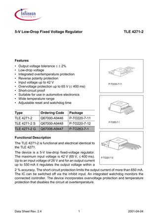
  • 1. P-TO220-7-11 P-TO263-7-1 P-TO220-7-12 5-V Low-Drop Fixed Voltage Regulator TLE 4271-2 Data Sheet Rev. 2.4 1 2001-04-04 Features • Output voltage tolerance ≤ ± 2% • Low-drop voltage • Integrated overtemperature protection • Reverse polarity protection • Input voltage up to 42 V • Overvoltage protection up to 65 V (≤ 400 ms) • Short-circuit proof • Suitable for use in automotive electronics • Wide temperature range • Adjustable reset and watchdog time Functional Description The TLE 4271-2 is functional and electrical identical to the TLE 4271. The device is a 5-V low-drop fixed-voltage regulator. The maximum input voltage is 42 V (65 V, ≤ 400 ms). Up to an input voltage of 26 V and for an output current up to 550 mA it regulates the output voltage within a Type Ordering Code Package TLE 4271-2 Q67000-A9446 P-TO220-7-11 TLE 4271-2 S Q67000-A9448 P-TO220-7-12 TLE 4271-2 G Q67006-A9447 P-TO263-7-1 2 % accuracy. The short circuit protection limits the output current of more than 650 mA. The IC can be switched off via the inhibit input. An integrated watchdog monitors the connected controller. The device incorporates overvoltage protection and temperature protection that disables the circuit at overtemperature.
  • 2. TLE 4271-2 Data Sheet Rev. 2.4 2 2001-04-04 Figure 1 Pin Configuration (top view) Pin Definitions and Functions Pin Symbol Function 1 I Input; block to ground directly on the IC with ceramic capacitor. 2 INH Inhibit 3 RO Reset Output; the open collector output is connected to the 5 V output via an integrated resistor of 30 kΩ. 4 GND Ground 5 D Reset Delay; connect a capacitor to ground for delay time adjustment. 6 WI Watchdog Input 7 Q 5-V Output; block to ground with 22 µF capacitor, ESR < 3 Ω. AEP01939 GND INH Ι RO WI D Q 1 7 GND INH Ι RO 1 WI AEP02017 D Q 7 AEP01938 INH RO GND 1 7 WI D Ι Q P-TO220-7-11 P-TO263-7-1 P-TO220-7-12
  • 3. TLE 4271-2 Data Sheet Rev. 2.4 3 2001-04-04 Circuit Description The control amplifier compares a reference voltage, which is kept highly accurate by resistance adjustment, to a voltage that is proportional to the output voltage and drives the base of a series transistor via a buffer. Saturation control as a function of the load current prevents any over-saturation of the power element. The reset output RO is in high-state if the voltage on the delay capacitor CD is greater or equal VUD. The delay capacitor CD is charged with the current ID for output voltages greater than the reset threshold VRT. If the output voltage gets lower than VRT (’reset condition’) a fast discharge of the delay capacitor CD sets in and as soon as VD gets lower than VLD the reset output RO is set to low-level. The time for the delay capacitor charge from VUD to VLD is the reset delay time tD. When the voltage on the delay capacitor has reached VUD and reset was set to high, the watchdog circuit is enabled and discharges CD with the constant current IDWD. If there is no rising edge observed at the watchdog input, CD will be discharge down to VLDW, then reset output RO will be set to low and CD will be charged again with the current IDWC until VD reaches VUD and reset will be set high again. If the watchdog pulse (rising edge at watchdog input WI) occurs during the discharge period CD is charged again and the reset output stays high. After VD has reached VUD, the periodical behavior starts again. Internal protection circuits protect the IC against: • Overload • Overvoltage • Overtemperature • Reverse polarity
  • 4. TLE 4271-2 Data Sheet Rev. 2.4 4 2001-04-04 Figure 2 Block Diagram Temperature Sensor Saturation Control and Protection Circuit + - Reference Bandgap Adjustment Reset Generator Watchdog 4 2 1 7 3 5 6 INH GND WI AEB01940 Control Amplifier Buffer Ι Q D RO
  • 5. TLE 4271-2 Data Sheet Rev. 2.4 5 2001-04-04 Absolute Maximum Ratings Tj = – 40 to 150 °C Parameter Symbol Limit Values Unit Notes min. max. Input Voltage Voltage Current VI VI II – 42 – – 42 65 – V V mA – t ≤ 400 ms internally limited Inhibit Voltage Voltage Current VINH VINH IINH – 42 – – 42 65 – V V mA – t ≤ 400 ms internally limited Reset Output Voltage Current VRO IRO – 0.3 – 42 – V mA – internally limited Reset Delay Voltage Current VD ID – 0.3 – 5 7 5 V mA – – Watchdog Voltage Current VW IW – 0.3 – 5 7 5 V mA – – Output Voltage Current VQ IQ – 1.0 – 5 16 – V mA – internally limited Ground Current IGND – 0.5 – A – Temperatures Junction temperature Storage temperature Tj Tstg – – 50 150 150 °C °C – –
  • 6. TLE 4271-2 Data Sheet Rev. 2.4 6 2001-04-04 Operating Range Parameter Symbol Limit Values Unit Notes min. max. Input voltage VI 6 40 V – Junction temperature Tj – 40 150 °C – Thermal Resistance Junction ambient Rthja – 65 70 K/W K/W – P-TO263 Junction case Rthjc Zthjc – – 3 2 K/W K/W – t < 1 ms
  • 7. TLE 4271-2 Data Sheet Rev. 2.4 7 2001-04-04 Characteristics VI = 13.5 V; – 40 °C ≤ Tj = ≤ 125 °C; VINH > VU,INH (unless otherwise specified) Parameter Symbol Limit Values Unit Test Condition min. typ. max. Output voltage VQ 4.90 5.00 5.10 V 5 mA ≤ IQ ≤ 550 mA; 6 V ≤ VI ≤ 26 V Output voltage VQ 4.90 5.00 5.10 V 26 V ≤ VI ≤ 36 V; IQ ≤ 300 mA; Output current limiting IQmax 650 800 – mA VQ = 0 V Current consumption Iq = II Iq – – 6 µA VINH = 0 V; IQ = 0 mA Current consumption Iq = II Iq – 800 – µA VINH = 5 V; IQ = 0 mA Current consumption Iq = II – IQ Iq – 1 1.5 mA IQ = 5 mA Current consumption Iq = II – IQ Iq – 55 75 mA IQ = 550 mA Current consumption Iq = II – IQ Iq – 70 90 mA IQ = 550 mA; VI = 5 V Drop voltage Vdr – 350 700 mV IQ = 550 mA1) Load regulation ∆VQ – 25 50 mV IQ = 5 to 550 mA; VI = 6 V Supply voltage regulation ∆VQ – 12 25 mV VI = 6 to 26 V IQ = 5 mA Power supply Ripple rejection PSRR – 54 – dB fr = 100 Hz; Vr = 0.5 VPP 1) Drop voltage = VI – VQ (measured when the output voltage has dropped 100 mV from the nominal value obtained at 13.5 V input)
  • 8. TLE 4271-2 Data Sheet Rev. 2.4 8 2001-04-04 Reset Generator Switching threshold VRT 4.5 4.65 4.8 V – Reset high voltage VROH 4.5 – – V – Saturation voltage VRO,SAT – 60 – mV Rintern = 30 kΩ; 1.0 V ≤ VQ ≤ 4.5 V Saturation voltage VRO,SAT – 200 400 mV IR = 3 mA1) ; VQ = 4.4 V Reset pull-up R 18 30 46 KΩ internally connected to Q Lower reset timing threshold VLD 0.2 0.45 0.8 V VQ < VRT Charge current ID 8 14 25 µA VD = 1.0 V Upper timing threshold VUD 1.4 1.8 2.3 V – Delay time tD 8 13 18 ms CD = 100 nF Reset reaction time tRR – – 3 µs CD = 100 nF Overvoltage Protection Turn-off voltage VI, ov 40 44 46 V – Inhibit Turn-on voltage VU,INH 1.0 2.0 3.5 V VQ = high (> 4.5 V) Turn-off voltage VL,INH 0.8 1.3 3.3 V VQ = low (< 0.8 V) Inhibit current IINH 8 12 25 µA VINH = 5 V 1) Test condition not applicable during delay time for power-on reset. Characteristics (cont’d) VI = 13.5 V; – 40 °C ≤ Tj = ≤ 125 °C; VINH > VU,INH (unless otherwise specified) Parameter Symbol Limit Values Unit Test Condition min. typ. max.
  • 9. TLE 4271-2 Data Sheet Rev. 2.4 9 2001-04-04 Watchdog Upper watchdog switching threshold VUDW 1.4 1.8 2.3 V – Lower watchdog switching threshold VLDW 0.2 0.45 0.8 V – Discharge current IDWD 1.5 2.7 3.5 µA VD = 1 V Charge current IDWC 8 14 25 µA VD = 1 V Watchdog period tWD,P 40 55 80 ms CD = 100 nF Watchdog trigger time tWI,tr 30 45 66 ms CD = 100 nF see diagram Watchdog pulse slew rate VWI 5 – – V/µs from 20% to 80% VQ Characteristics (cont’d) VI = 13.5 V; – 40 °C ≤ Tj = ≤ 125 °C; VINH > VU,INH (unless otherwise specified) Parameter Symbol Limit Values Unit Test Condition min. typ. max.
  • 10. TLE 4271-2 Data Sheet Rev. 2.4 10 2001-04-04 Figure 3 Test Circuit Figure 4 Circuit 3 2 V VΙ VINH Ι C D Ι D 5 D 4 WI GND V 6 AES01941 RO V VQ 470 nF 1000 F Ι µ Ι Ι TLE 4271-2 1 7 Q 22 F RO µ Ι 22 F to MC Reset 3 4 5 100 nF AES01942 µ 470 nF Input TLE 4271-2 1 7 5 V-Output 6 2 e.g. KL 15 Input Watchdog Signal from MC
  • 11. TLE 4271-2 Data Sheet Rev. 2.4 11 2001-04-04 Application Description The IC regulates an input voltage in the range of 6 V < VI < 40 V to VQnom = 5.0 V. Up to 26 V it produces a regulated output current of more than 550 mA. Above 26 V the save- operating-area protection allows operation up to 36 V with a regulated output current of more than 300 mA. Overvoltage protection limits operation at 42 V. The overvoltage protection hysteresis restores operation if the input voltage has dropped below 36 V. The IC can be switched off via the inhibit input, which causes the quiescent current to drop below 50 µA. A reset signal is generated for an output voltage of VQ < 4.5 V. The watchdog circuit monitors a connected controller. If there is no positive-going edge at the watchdog input within a fixed time, the reset output is set to low. The delay for power-on reset and the maximum permitted watchdog-pulse period can be set externally with a capacitor. Design Notes for External Components An input capacitor CI is necessary for compensation of line influences. The resonant circuit consisting of lead inductance and input capacitance can be damped by a resistor of approx. 1 Ω in series with CI. An output capacitor CQ is necessary for the stability of the regulating circuit. Stability is guaranteed at values of CQ ≥ 22 µF and an ESR of < 3 Ω. Reset Circuitry If the output voltage decreases below 4.5 V, an external capacitor CD on pin D will be discharged by the reset generator. If the voltage on this capacitor drops below VDRL, a reset signal is generated on pin RO, i.e. reset output is set low. If the output voltage rises above the reset threshold, CD will be charged with constant current. After the power-on- reset time the voltage on the capacitor reaches VDU and the reset output will be set high again. The value of the power-on-reset time can be set within a wide range depending of the capacitance of CD. Reset Timing The power-on reset delay time is defined by the charging time of an external capacitor Cd which can be calculated as follows: tD = CD∗∆V/ID Definitions: CD = delay capacitor tD = reset delay time ID = charge current, typical 14 µA ∆V = VUD, typical 1.8 V VUD = upper delay timing threshold at CD for reset delay time
  • 12. TLE 4271-2 Data Sheet Rev. 2.4 12 2001-04-04 The reset reaction time trr is the time it takes the voltage regulator to set the reset out LOW after the output voltage has dropped below the reset threshold. It is typically 1 µs for delay capacitor of 47 nF. For other values for Cd the reaction time can be estimated using the following equation: tRR ≈ 20 s/F × Cd Figure 5 Time Response AET01985 t D t RR RR t < Power Reset Shutdown Thermal Voltage Drop at Input Undervoltage at Output Secondary Spike Bounce Load Shutdown on VRO, SAT LD V UD V VD, SAT RT V L, INH V VU, INH INH V RO V VD Q V Ι V t t t t t = dt V d D D C Ι
  • 13. TLE 4271-2 Data Sheet Rev. 2.4 13 2001-04-04 Watchdog Timing Figure 6 Time Response, Watchdog Behavior AES03078 WD, P t t WD, L D V VQ VΙ VR WΙ V WΙ, tr t UDW V = -VLDW ( ) UDW V -VLDW ( ) ΙDWD ΙDWC t = WD, L CD WΙ, tr t WD, P t UDW V = -VLDW ( ) ( ) ΙDWC +ΙDWD Ι . DWC ΙDWD CD C ; D ; UDW V VLDW
  • 14. TLE 4271-2 Data Sheet Rev. 2.4 14 2001-04-04 Typical Performance Characteristics Output Voltage VQ versus Temperature Tj Output Voltage VQ versus Input Voltage VI (VINH = VI) AED01928 -40 0 40 80 120 ˚C 160 4.6 j T Q V VI = 13.5 V 4.7 4.8 4.9 5.0 5.1 V 5.2 R 6 4 2 0 4 0 2 8 12 10 Q V V 10 V 6 8 VΙ AED01929 = 25 L Ω
  • 15. TLE 4271-2 Data Sheet Rev. 2.4 15 2001-04-04 Output Current Limit IQ versus Temperature Tj Current Consumption Iq versus Output Current IQ Output Current IQ versus Input Voltage VI Current Consumption Iq versus Output Current IQ AED01930 -40 0 40 80 120 ˚C 160 0 j T 200 400 600 800 1000 mA 1200 Q max I 0 0 AED03076 Ι q mA = 13.5 V mA Ι V 20 40 60 80 120 Q Ι 1 2 3 4 5 6 AED01931 0 10 20 30 40 V 50 0 0.4 0.8 1.2 A 1.0 0.6 0.2 I V IQ = 125 ˚C Tj 25 ˚C 0 0 AED03077 Ι q mA = 13.5 V mA Ι V 100 200 300 400 600 Q Ι 10 20 30 40 50 60 70 80
  • 16. TLE 4271-2 Data Sheet Rev. 2.4 16 2001-04-04 Current Consumption Iq versus Input Voltage VI Inhibit Current IINH versus Inhibit Voltage VINH Drop Voltage Vdr versus Output Current IQ Output Voltage VQ versus Inhibit Voltage VINH AED01934 0 10 20 30 40 V 50 0 40 80 120 mA 100 60 20 I V Iq 20 Ω L R = 10 Ω 50 Ω RL = 0 0 1 6 3 2 INH AED01944 4 V 2 4 6 8 10 12 VΙ = 13.5 V = 25 C j T INH, high Ι Ι INH, on Ι INH, off 5 INH V µA Ι 400 200 300 100 200 0 400 0 800 600 700 500 Dr V mV mA 600 1000 Ι Q AED02755 T = 125 C j T = 25 C j 3 3 2 1 0 0 1 2 6 5 4 V 5 V 4 6 VINH = 25 C = 13.5 V Ι j V T AED01945 Q V
  • 17. TLE 4271-2 Data Sheet Rev. 2.4 17 2001-04-04 Inhibit Current Consumptions IINH versus Temperature T Switching Voltage VUD and VLDW versus Temperature T Inhibit Voltages VINH versus Temperature Tj -40 0 0 120 80 40 T j A 14 AED01946 160 Ι INH µ 2 4 6 8 10 12 Ι INH, high Ι INH, on Ι INH, off UD 40 -40 0 0 V V V UDW , V VΙ 160 C 80 120 T j AED01948 = 13.5 V 1.2 0.8 0.4 1.6 2.4 2.0 LDW V 3 2 1 40 -40 0 0 4 V 6 5 INH 160 C 80 120 AED01947 j T V VINH, on INH, off V
  • 18. TLE 4271-2 Data Sheet Rev. 2.4 18 2001-04-04 Charge Current ID, IDWC and Discharge Current IDWD versus Temperature Tj Watchdog Pulse Time Tw versus Temperature Tj AED01949 -40 0 I V = 13.5 V 2 4 6 8 10 12 14 16 µA 0 40 80 120 160 ˚C I Tj = 1 V D V D I , IDWC IDWD 80 40 -40 0 10 30 20 40 0 50 60 70 80 160 120 C T j = 13.5 V AED01950 Ι CD V = 100 nF ms W T
  • 19. TLE 4271-2 Data Sheet Rev. 2.4 19 2001-04-04 Package Outlines ±0.1 1.27 4.4 9.25 ±0.2 0.05 2.4 0.5±0.1 ±0.3 8.6 10.2 ±0.3 ±0.4 3.9 ±0.4 8.4 3.7 ±0.3 A A 0.25 M 2.8 1) 15.65 ±0.3 12.95 0...0.15 1.27 0.6±0.1 C ±0.2 17 ±0.3 8.51) 9.9±0.2 7x -0.15 3.7 10±0.2 6x C 1.6 ±0.3 All metal surfaces tin plated, except area of cut. Metal surface min. X=7.25, Y=12.3 Typical 1) 0...0.3 P-TO220-7-11 (Plastic Transistor Single Outline Package) GPT09083 Sorts of Packing Package outlines for tubes, trays etc. are contained in our Data Book “Package Information”. Dimensions in mm
  • 20. TLE 4271-2 Data Sheet Rev. 2.4 20 2001-04-04 A B A 0.25 M 9.9±0.2 1) 15.65 ±0.3 12.95 0...0.15 1.27 0.6±0.1 ±0.1 1.27 4.4 B 9.25 ±0.2 0.05 C 17 ±0.3 8.51) 10±0.2 C 2.4 0.5±0.1 13 ±0.5 ±0.5 11 7x 0...0.3 6x All metal surfaces tin plated, except area of cut. Metal surface min. X=7.25, Y=12.3 1) Typical 2.4 3.7 -0.15 ±0.2 2.8 P-TO220-7-12 (Plastic Transistor Single Outline Package) GPT09084 Sorts of Packing Package outlines for tubes, trays etc. are contained in our Data Book “Package Information”. Dimensions in mm
  • 21. TLE 4271-2 Data Sheet Rev. 2.4 21 2001-04-04 A 8˚ max. B A 0.25 M 0.1 Typical ±0.2 10 8.51) 7.55 1) (15) ±0.2 9.25 ±0.3 1 0...0.15 7x0.6±0.1 ±0.1 1.27 4.4 B 0.5±0.1 ±0.3 2.7 4.7 ±0.5 0.05 1) 0.1 Metal surface min. X=7.25, Y=6.9 2.4 1.27 All metal surfaces tin plated, except area of cut. 0...0.3 B 6x P-TO263-7-1 (Plastic Transistor Single Outline Package) GPT09114 Sorts of Packing Package outlines for tubes, trays etc. are contained in our Data Book “Package Information”. Dimensions in mm SMD = Surface Mounted Device
  • 22. TLE 4271-2 Data Sheet Rev. 2.4 22 2001-04-04
  • 23. TLE 4271-2 Data Sheet Rev. 2.4 23 2001-04-04 Edition 2001-04-04 Published by Infineon Technologies AG, St.-Martin-Strasse 53, D-81541 München, Germany © Infineon Technologies AG 2001. All Rights Reserved. Attention please! The information herein is given to describe certain components and shall not be consid- ered as warranted characteristics. Terms of delivery and rights to technical change reserved. We hereby disclaim any and all warranties, including but not limited to warranties of non- infringement, regarding circuits, descriptions and charts stated herein. Infineon Technologies is an approved CECC manufacturer. Information For further information on technology, deliv- ery terms and conditions and prices please contact your nearest Infineon Technologies Office in Germany or our Infineon Technolo- gies Representatives worldwide (see ad- dress list). Warnings Due to technical requirements components may contain dangerous substances. For in- formation on the types in question please contact your nearest Infineon Technologies Office. Infineon Technologies Components may only be used in life-support devices or systems with the express written approval of Infineon Technologies, if a failure of such components can reasonably be expected to cause the fail- ure of that life-support device or system, or to affect the safety or effectiveness of that de- vice or system. Life support devices or sys- tems are intended to be implanted in the hu- man body, or to support and/or maintain and sustain and/or protect human life. If they fail, it is reasonable to assume that the health of the user or other persons may be endangered.