

Recommended
More Related Content
What's hot
What's hot (20)
Similar to Robotics and automation rat 203
Similar to Robotics and automation rat 203 (20)
Recently uploaded
Recently uploaded (20)
Robotics and automation rat 203
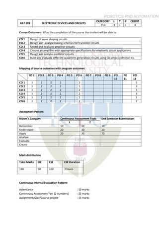
- 1. RAT 203 ELECTRONIC DEVICES AND CIRCUITS CATEGORY L T P CREDIT PCC 3 1 0 4 Course Outcomes: After the completion of the course the student will be able to CO 1 Design of wave shaping circuits CO 2 Design and analyse biasing schemes for transistor circuits CO 3 Model and evaluate amplifier circuits CO 4 Choose an amplifier with appropriate specifications for electronic circuit applications CO 5 Design and analyse oscillator circuits CO 6 Build and evaluate different waveform generation circuits using Op-amps and timer ICs Mapping of course outcomes with program outcomes PO 1 PO 2 PO 3 PO 4 PO 5 PO 6 PO 7 PO 8 PO 9 PO 10 PO 11 PO 12 CO 1 3 2 2 2 2 3 CO 2 3 2 2 2 1 3 CO 3 3 2 2 2 2 3 CO 4 3 2 2 2 2 3 CO 5 3 2 2 2 2 3 CO 6 3 2 2 2 2 3 Assessment Pattern Bloom’s Category Continuous Assessment Tests End Semester Examination 1 2 Remember 10 10 10 Understand 20 20 20 Apply 20 20 70 Analyse Evaluate Create Mark distribution Total Marks CIE ESE ESE Duration 150 50 100 3 hours Continuous Internal Evaluation Pattern: Attendance : 10 marks Continuous Assessment Test (2 numbers) : 25 marks Assignment/Quiz/Course project : 15 marks ROBOTICS AND AUTOMATION
- 2. End Semester Examination Pattern: There will be two parts; Part A and Part B. Part A contain 10 questions with 2 questions from each module, having 3 marks for each question. Students should answer all questions. Part B contains 2 questions from each module of which student should answer any one. Each question can have maximum 2 sub-divisions and carry 14 marks. Module 1 Diode Circuits: Clipping circuits- Single level and two level clippers, Clamping circuits-Design of Zener voltage regulators BJT biasing circuits: DC load line, Operating point of a BJT, Factors affecting stability of Q point, Fixing of operating point. Biasing circuits - fixed bias, collector feedback bias, emitter bias and voltage divider bias, Bias compensation using diode and thermistor, Low frequency equivalent circuit of BJT. Common Emitter amplifier - Role of coupling and emitter bypass capacitors – AC Equivalent Circuit – h parameter model of BJT -Amplifier gains and impedances calculations using h equivalent circuit Module 2 Field effect Transistors: Review of JFET and MOSFET construction, working and characteristics- Biasing a JFET and MOSFET using voltage divider bias–- CS and CD amplifiers – small signal models- FET as switch and voltage controlled resistance. Frequency response of Amplifiers: Frequency Response characteristics of BJT and FET amplifier, Low frequency and High frequency analysis of BJT (Common Emitter) and FET (Common Source) amplifier : Miller effect capacitance, Miller’s Theorem, Gain bandwidth product, hybrid Pi Model of BJT amplifier Module 3 Multistage amplifiers: Different types of coupling - Direct, RC, & transformer coupled amplifiers - operation, advantages and disadvantages (Analysis not required) Power amplifiers using BJT: Class A, Class B, Class AB and Class C power amplifiers, Conversion efficiency and distortion in power amplifiers Feedback amplifiers: Positive and negative feedback, Effect of negative feedback on gain, input impedance, output impedance, band width and distortion, Basic feedback topologies - Gain, input and output impedance with feedback Module 4 Oscillators: Oscillator operation, Bark Hausen’s criterion, RC oscillators – working of BJT based RC phase shift and Wien bridge oscillators, LC Oscillators - working of BJT based Hartley, Colpitts - with derivation of frequency of oscillation for the above mentioned oscillators and Crystal oscillators Operational amplifiers: Introduction, Basic block diagram, Ideal op-amp, transfer characteristics and op-amp parameters, gain, CMRR, slew rate etc, Equivalent circuit of ideal and practical op-amp, op-amp configurations- Open loop and closed loop configurations, -properties of ideal and practical opamp. Basic Op-amp Circuits: Inverting and non-inverting amplifier, Scale changer, Voltage follower, Summing amplifier, Subtractor, Adder-subtractor Module 5 Op-amp applications: Differential amplifier with single op-amp, Instrumentation amplifier, Integrators, Differentiators, Comparators, Zero crossing detector, Schmitt trigger; square, triangular and ramp generator using opamp, Effect of slew rate on wave form generation. ROBOTICS AND AUTOMATION
- 3. Specialized ICs and their applications: Timer IC 555 - Block Diagram of IC 555, Astable and Monostable operations Phase Locked Loop - Block Diagram of PLL IC 565, Operation, Lock and capture range Voltage Regulators - Fixed voltage regulators, 78XX and 79XX series, Adjustable voltage regulators, IC 723 Voltage regulator. Text Books 1. Robert L. Boylestad and Louis Nashelsky, “Electronic Devices and Circuit Theory”, Pearson Education India, 11/e, 2013 2. Albert Malvino and David J. Bates, “Electronic Principles”, Tata McGraw-Hill, 7/e, 2007 3. Gayakwad R. A., “Op-Amps and Linear Integrated Circuits”, Pearson Education India, 4/e, 2015 4. Salivahanan S. and V. S. Kanchana Bhaaskaran, “Linear Integrated Circuits”, McGraw Hill Education India, 2/e, 2015 Reference Books 1. Sedra A.S. and Smith K.C., “Microelectronics Circuits-Theory and Applications”, Oxford University Press, 6/e, 2011 2. Jacob Millman and Arvin Grabel, “Micro Electronics”, Tata McGraw-Hill, 2/e, 1999 3. Donald A. Neamen, “Electronic Circuits-Analysis and Design”, McGraw Hill Education India, 3/e, 2007 Course Contents and Lecture Schedule No Topic No. of Lectures 1 MODULE 1 1.1 Diode Circuits: Clipping circuits- Single level and two-level clippers, Clamping circuits-Design of Zener voltage regulators 3 1.2 BJT biasing circuits: DC load line, Operating point of a BJT, Factors affecting stability of Q point, Fixing of operating point. Biasing circuits - fixed bias, collector feedback bias, emitter bias and voltage divider bias, Bias compensation using diode and thermistor, Low frequency equivalent circuit of BJT. Common Emitter amplifier - Role of coupling and emitter bypass capacitors – AC Equivalent Circuit – h parameter model of BJT -Amplifier gains and impedances calculations using h equivalent circuit 7 2 MODULE 2 2.1 Field effect Transistors: Review of JFET and MOSFET construction, working and characteristics, Biasing a JFET and MOSFET using voltage divider bias, CS and CD amplifiers, small signal models-FET as switch and voltage controlled resistance. 4 2.2 Frequency response of Amplifiers Frequency Response characteristics of BJT and FET amplifier Low frequency and High frequency analysis of BJT (Common Emitter) and FET (Common Source)amplifier Miller effect capacitance, Miller’s Theorem, Gain bandwidth product, hybrid Pi Model of BJT amplifier 5 3 MODULE 3 ROBOTICS AND AUTOMATION
- 4. 3.1 Multistage amplifiers: Different types of coupling - Direct, RC, & transformer coupled amplifiers -operation, advantages and disadvantages (Analysis not required) 1 3.2 Power amplifiers using BJT: Class A, Class B, Class AB and Class C power amplifiers, Conversion efficiency and distortion in power amplifiers. 3 3.3 Feedback amplifiers: Positive and negative feedback, Effect of negative feedback on gain, input impedance, output impedance, band width and distortion, Basic feedback topologies - Gain, input and output impedance with feedback 4 4 MODULE 4 4.1 Oscillators: Oscillator operation, Bark Hausen’s criterion, RC oscillators – working of BJT based RC phase shift and Wien bridge oscillators, LC Oscillators - working of BJT based Hartley, Colpitts - with derivation of frequency of oscillation for the above mentioned oscillators and Crystal oscillators. 4 4.2 Operational amplifiers: Introduction, Basic block diagram, Ideal op-amp transfer characteristics and op-amp parameters, gain, CMRR, slew rate etc Equivalent circuit of ideal and practical op-amp, op-amp configurations- Open loop and closed loop configurations, -properties of ideal and practical opamp. 3 4.3 Basic Op-amp Circuits: Inverting and non-inverting amplifier, Scale changer, Voltage follower, Summing amplifier, Subtractor, Adder-subtractor 2 5 MODULE 5 5.1 Op-amp applications: Differential amplifier with single op-amp, Instrumentation amplifier-derivation of gain Integrators, Differentiators, Comparators, Zero crossing detector, Schmitt trigger; square, triangular and ramp generator using opamp, Effect of slew rate on wave form generation. 4 5.2 Specialized ICs and their applications: Timer IC 555 - Block Diagram of IC 555, Astable and Monostable operations 2 5.3 Phase Locked Loop - Block Diagram of PLL IC 565, Operation, Lock and capture range. 1 5.4 Voltage Regulators - Fixed voltage regulators, 78XX and 79XX series, Adjustable voltage regulators, IC 723 Voltage regulator 2 ROBOTICS AND AUTOMATION
- 5. MODEL QUESTION PAPER APJ ABDUL KALAM TECHNOLOGICAL UNIVERSITY THIRD SEMESTER B.TECH. DEGREE EXAMINATION Course Code: RAT 203 Course Name: ELECTRONIC DEVICES AND CIRCUITS Max. Marks: 100 Duration: 3 Hours PART A Answer all questions, each carries 3 marks. Marks 1 A positive voltage clamping circuit and a positive shunt clipping circuit each have a ± 5V square wave input. Sketch the output waveform of each circuit. (3 ) 2 Draw the h parameter model of BJT. (3 ) 3 In a CE amplifier circuit, hfe =50, hie =1.3kΩ, Cbc= 5pF, RC =3kΩ, RL= 2.2 kΩ. Calculate the Miller capacitance. (3 ) 4 Draw and Explain the drain characteristics of N channel Enhancement MOSFET. ( 3) 5 Compare different multistage amplifiers. ( 3) 6 Explain how cross over distortion is avoided in class AB amplifier. ( 3) 7 Design a Wein bridge oscillator to generate a sinusoidal waveform of 2 kHz. (3) 8 List the properties of ideal opamp. (3) 9 Explain the effect of slew rate on waveform generation. (3) 10 In an astable multivibrator using 555, RB = 750 Ω. Determine the values of RA and C to generate a 1.0 MHz clock that has a duty cycle of 25%. (3) PART B Answer any one full question from each module, each carries14 marks. MODULE1 11 a) Define operating point and explain the factors affecting the operating point stability. (6 ) b) Explain any one compensation technique used for reducing the drift of operating point. (8 ) 12 a) Design a voltage divider bias circuit to operate from 15 V supply. The bias conditions are to be VCE = VE = 5V and IC = 5mA. Assume the transistor β is 100. Calculate the stability factors of the designed circuit. ( 10) b) Explain the role of coupling and emitter bypass capacitors in amplifier circuits. (4 ) MODULE II 13 a) Draw the frequency response curve of CE amplifier and explain why the gain decreases at low and high frequencies (6 ) b) With a neat diagram explain the construction and characteristics of JFET. (8) 14 a) Using small signal model, derive the expression for Zi, Zo, AV, Ai of a CS amplifier circuit (10) b) Draw the hybrid pi model of BJT amplifier. (4) ROBOTICS AND AUTOMATION
- 6. MODULE III 15 a) Explain the effects of negative feedback. (6) b) Draw the circuit diagram and explain the working of two stage Transformer coupled amplifier. Discuss the important features and applications. (8) 16 a) Draw a negative voltage shunt feedback topology. Derive the Gain, input impedance and output impedance. (10) b) A transformer coupled class A power amplifier draws a current of 200mA from a collector supply of 10V, when no signal is applied to it. Determine i) Maximum output power ii) Maximum collector efficiency iii) Power rating of the transistor. ( 4) MODULE IV 17 a) Draw the circuit of Hartley oscillator and derive the frequency of oscillation. (8) b) Explain the working of op-amp inverting amplifier. Derive the expression for its voltage gain. (6) 18 a) Draw the circuit of a three channel summer amplifier and derive the expression for output voltage. Design a summer having gains of 5dB, 10 dB and 15dB respectively for each channel. (10) b) Explain the basic principle of oscillator. (4) MODULE V 19 a) Draw the elementary block diagram of PLL and explain. (8) b) Design a monostable multivibrator which produces an output pulse width of 1 ms using 555. (6) 20 a) Derive the overall gain in an instrumentation amplifier. (7) b) Draw the functional block diagram of IC 723 and explain its operation. (7) **** ROBOTICS AND AUTOMATION