Design and construction of a prototype wireless power transfer device
•
0 likes•245 views

Multidisciplinary Journal Supported by TETFund. The journals would publish papers covering a wide range of subjects in journal science, management science, educational, agricultural, architectural, accounting and finance, business administration, entrepreneurship, business education, all journals

Recommended
Recommended
More Related Content
What's hot
What's hot (20)
Similar to Design and construction of a prototype wireless power transfer device
Similar to Design and construction of a prototype wireless power transfer device (20)
More from Nuhu Bamalli Polytechnic Zaria
More from Nuhu Bamalli Polytechnic Zaria (20)
Recently uploaded
Recently uploaded (20)
Design and construction of a prototype wireless power transfer device
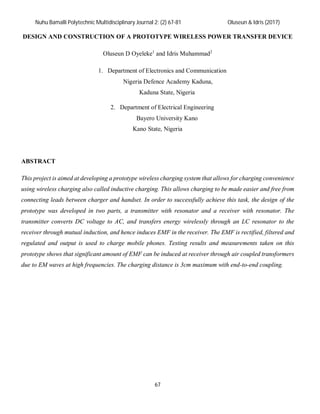
- 1. Nuhu Bamalli Polytechnic Multidisciplinary Journal 2: (2) 67-81 Oluseun & Idris (2017) 67 DESIGN AND CONSTRUCTION OF A PROTOTYPE WIRELESS POWER TRANSFER DEVICE Oluseun D Oyeleke1 and Idris Muhammad2 1. Department of Electronics and Communication Nigeria Defence Academy Kaduna, Kaduna State, Nigeria 2. Department of Electrical Engineering Bayero University Kano Kano State, Nigeria ABSTRACT This project is aimed at developing a prototype wireless charging system that allows for charging convenience using wireless charging also called inductive charging. This allows charging to be made easier and free from connecting leads between charger and handset. In order to successfully achieve this task, the design of the prototype was developed in two parts, a transmitter with resonator and a receiver with resonator. The transmitter converts DC voltage to AC, and transfers energy wirelessly through an LC resonator to the receiver through mutual induction, and hence induces EMF in the receiver. The EMF is rectified, filtered and regulated and output is used to charge mobile phones. Testing results and measurements taken on this prototype shows that significant amount of EMF can be induced at receiver through air coupled transformers due to EM waves at high frequencies. The charging distance is 3cm maximum with end-to-end coupling.
- 2. Nuhu Bamalli Polytechnic Multidisciplinary Journal 2: (2) 67-81 Oluseun & Idris (2017) 68 INTRODUCTION Wireless power transfer is an emerging technology in the world of mobile phones. Imagine a scenario where one gets home and one can simply place his/her phone on a charging mat in his sitting room or in the kitchen or in his vehicle without having to plug in his phone to a charging source using wires. During emergency one can use his hand free to communicate while ones phone is still charging. The convenience of wireless power transfer through the process of inductive coupling will change the way we charge mobile phones and other devices. WIRELESS CHARGING AND ELECTRONIC WARFARE Wireless power transfer can be used to power Electric cars, electronic gadgets for Electronic warfare and electronic attacks. In future drones, Quad copters, UAV, wearable devices, body implants and other devices used by security personnel will be powered wirelessly. We are in a wireless revolution, creating a world of wireless technologies is a possibility, a world where we are doing away with bio-degradable organic materials, a world where there will no more be bundles of wires, tangling up here and there, a neat world, where there will be invisible yet reliable interconnectivity between electronic components and their power source, wireless hardware, wireless keyboard, wireless mouse, Bluetooth, ZIGBEE, WLAN, WIFI are all aftermath of the emerging success of the current wireless revolution. Like a typical scene in a Sci-fi movie the world is gradually doing away with wires and using EM waves to establish connection. PROJECT AIM The Objective of this project is to design a prototype inductive wireless mobile phone power transfer charging system. The project exposes one to hand-on practical experience in building electronic circuits by appropriate choice of electronics devices and components. This also demonstrates the capability and practicability of wireless power transfer for charging electronic devices using mobile phone for demonstration.
- 3. Nuhu Bamalli Polytechnic Multidisciplinary Journal 2: (2) 67-81 Oluseun & Idris (2017) 69 PROJECT OBJECTIVES In other to realize this project, Study of existing technology was carried out which include hardware, schematics and existing wireless charger already in market. Proper research into the science of operation of wireless power transfer was carried out. The circuit was designed, modified, simulated and constructed. 1.7 System Block Diagram The system block diagram is shown in Figure 1.1 _ Figure 1.1 1.7 System Block Diagram The system block diagram is shown in Figure 1.1 DC Source Transmitter with Resonator M Receiver Resonator Rectifier Voltage Regulator Load Figure 1.1 Block diagram of prototype Charger Block diagram of prototype Charger DC source: the function of this block is the production of dc source voltage which can be from a car charger or dc battery of 12v. Transmitter with resonator: a high efficiency push-pull amplifier with lc resonator where the dc voltage is converted to a signal with frequency range between 50-70 kHz. Receiver resonator: the magnetic field produced by the transmitter combines to the receiver resonator, exciting the resonator therefore causing the buildup of energy in it. Rectifier: the rectifier changes the received AC energy from the receiver power back to dc power. Voltage regulator: the dc rectified voltage is regulated down to 5v suitable for mobile phones charging. Output: Output: this stage the energy is combined out of the device resonator to deliver energy, for example, powering a load directly or energy for battery charging. Output: this stage the energy is combined out of the device resonator to deliver energy, for example, powering a load directly or energy for battery charging. LITERATURE REVIEW Wireless charging is set to change this. We want to eradicate the problem of the dead battery, by providing power wirelessly so that anywhere with the vicinity of the wireless charger the phone can charge continuously even while in use.
- 4. Nuhu Bamalli Polytechnic Multidisciplinary Journal 2: (2) 67-81 Oluseun & Idris (2017) 70 According to WiTricity Corporation, [1] “wireless power transfer had succeeded to make these essential products more available, convenient, and reliable (in terms of availability of power to run them). The wireless power technology is very real” MUTUAL INDUCTANCE Induced EMF can be dynamically induced or statically induced, and therefore creating the ability of one coil or circuit to produce EMF in a nearby coil by induction when the current induced in the first coil changes [7], usually the conductors or coils remain stationery and the flux linked with it is changed by oscillation. The self-inductance of each distinct coil is given as: L1 and L2 self-inductance [8] And Then by cross- multiplying the above equations, the existence of the mutual inductance between the both coils can be expressed in terms of the self-inductance of each coil. [8] 21 2 LLM Hence giving us a final and more common expression for the mutual inductance that exists between two coils as: [8
- 5. Nuhu Bamalli Polytechnic Multidisciplinary Journal 2: (2) 67-81 Oluseun & Idris (2017) 71 21 LLm In Henrys COEFFICIENT OF COUPLING K is called the coefficiant of coupling it is an expression of the fraction of the flux on one coil that will pass through the other coil, and it depends on the portion of the aggregate lines of flux lines that cuts both windings in the primary and secondary [9] .If the flux due to one coil completely links the other then the value of k is unity but if there is no linkage then the value of k is 0. When k=1 coils are said to be tightly coupled and when k=0 they are magentically isolated from each other and if k < 0.5 the two coils are said to be loosely coupled [10] . Coupling Factor between Coils Or H When the coefficient of coupling, k is equal to 1, such that all the magnetic flux lines of one coil cuts all of the turns of the other coil, the mutual inductance is equal to the geometric average of the two individual inductances of the coils [11] OSCILLATORS An electronic oscillator is an electronic circuit that produces a periodic, oscillating electronic signal, often a sine wave or a wave. [12] Oscillators are circuits that generate a voltage output waveform that is continuous at a selected frequency or frequency range, with the values of the inductors, capacitors or resistors forming a frequency tuneable LC resonant tank circuit and feedback network. The output of an oscillator depends on the device parameters and external components. In LC oscillators a tuned circuit is used to select frequency of interest. The LC oscillator’s frequency is controlled using a selective or resonant inductive/capacitive (LC) circuit with the resulting output frequency which is called the Frequency of Oscillation. An RLC circuit as shown in Figure 2.2 is a common oscillator arrangement. L R C
- 6. Nuhu Bamalli Polytechnic Multidisciplinary Journal 2: (2) 67-81 Oluseun & Idris (2017) 72 Figure 2.2 RLC Circuit Solution to the 2nd order differential equation is V=Voe-αt e +jwt Equation indicates oscillatory sinusoidal wave e +jwt having decaying amplitude with attenuation constant α The frequency output is given by ῲ = − [12] To keep the oscillations going in an LC tank circuit, all the energy lost in each oscillation has to be replaced and also retains at constant level the amplitude of these oscillations. The simplest way of replacing this lost energy is to take part of the output from the LC tank circuit, amplify it and then feed it back into the LC circuit again. This process can be achieved using a voltage amplifier using an op-amp, FET or bipolar transistor as its active device. If the energy replaced is too large the amplitude would increase until clipping of the supply rails occurs. Alternatively, if the quantity of energy exchanged is not sufficiently large enough, the amplitude would eventually damp out to zero over time and this will result in total loss of positive feedback energy and oscillations would stop ῲ = 1 LC Since ῳ =2πf LC f 2 1 Where: L is the Inductance in Henries. C is the Capacitance in Farads. ƒ is the Output Frequency in Hertz. THE SOURCE RESONATOR: THE ZVS DRIVER OSCILLATOR MODEL
- 7. Nuhu Bamalli Polytechnic Multidisciplinary Journal 2: (2) 67-81 Oluseun & Idris (2017) 73 This project uses a special type of Oscillator called the ZERO VOLTAGE SWITCHING ZVS (Mazilli) Driver designed by VladimiroMazilli[13] as the source resonator.This is a model of the ZVS Oscillator similar to the one used to build the circuit is shown in Figure 2.3 Figure 2.3 ZVS Mazilli Driver The ZVS is a push pull oscillator. In its purist sense it would consist of nothing more than two MOSFET, a capacitor, and an inductor L2. . The driver depends on the fact that no two components are precisely alike and uses small variances in the internal resistances of the MOSFETs’ and other properties to start the oscillation. The inductor L2 prevents AC from getting back to the batteries. The fast diodes prevent the FETS from turning on when they shouldn’t and going suicidal. Excessive voltage may reach the gate of the MOSFETs and destroy them therefore we need the rest of the supplementary components act as gate protection to make sure these does not happen . In operation the capacitor and inductor form an LC circuit, frequency that the driver operates at can be varied by changing the value of the capacitor and/or the number of turns on the primary. The zero voltage switching drivers is an inverter and has the benefit that it reduces the harmonic spectrum of any EMI (centering it on the switching frequency) and allows higher frequency operation causing reduced, easier-to-filter noise and the utilization of smaller filter components. ZVS stands for Zero Voltage Switching, which means switching, when voltage is equal to zero, giving no switching losses because the MOSFETs switch when they have zero volts across them. A “ZVS driver” can oscillate a large amount of power with about 90% efficiency and frequency range between 50-60 kHz. In order to prevent the oscillator from drawing huge peak currents and exploding, L1 is added in series with +V as a choke. The LC impedance is what limits the actual current (the choke just mitigates current spikes).[13]
- 8. Nuhu Bamalli Polytechnic Multidisciplinary Journal 2: (2) 67-81 Oluseun & Idris (2017) 74 The resonating frequency LC f 2 1 ENERGY TRANSFER Q FACTOR AND EFFICIENCY The general principle is that if a given oscillating amount of energy (for example a pulse or a series of pulses) is placed into a primary coil which is loaded capacitively; the coil will 'ring', forming an oscillating magnetic field. The energy will transfer back and forth as an exchange between the magnetic field in the inductor and the electric field across the capacitor at the resonant frequency. This oscillation will eventually die away at a rate determined by the gain-bandwidth (Q factor). The primary coil forms a RLC circuit, and the Q factor for such a coil is: [14] C L R Q 1 For R=10 Ω, C=1µF and L=10 mH, Q is given as 10. The quality factor is a ratio of the inductance to the resistance. The ratio of energy stores to the ratio of energy loss at resonance Q= [14] To the electronics and communication engineer the degree of predomination of the energy oscillation is important since the better the ratio of predominance then the better the circuit is able to accept current, and the better the current that is delivered to the charging device at the receiver output with power at the resonant frequency .The degree of predominance is given by a factor of goodness termed the Q factor. The graph of the bandwidth of a parallel resonance circuit is shown below in Figure 2.4
- 9. Nuhu Bamalli Polytechnic Multidisciplinary Journal 2: (2) 67-81 Oluseun & Idris (2017) 75 Figure 2.4 Bandwidth of a parallel resonance circuit Because from experimental results the Q factor can be very high, (around a thousand has been verified with air cored coils) only a small percentage of the field has to be coupled from one coil to the other to achieve high efficiency, It can be shown that a figure of merit for the efficiency is 21QQKU where Q1 and Q2 are the Q factor of the source and receiver coils. And the maximum achievable efficiency is [16] 2 2 2 11 U U opt CONSTRUCTION OF THE TRANSMITTER The Mazzilli ZVS driver is used due to its simplicity. However, in this case, the reason it works is because the ZVS driver begins by oscillating at around 50 - 60 khz. Since the objective is to build a transmitter resonator with frequency range of 50-70 kHz The ZVS Mazilli oscillator design is suitable, and also turn on and off when the voltage across them is zero. (Meaning, they generate little/no heat due to switching losses). The transmitter is made up of DC source, inverter and resonant tank circuit as shown in Figure 3.2 Figure 3.2 Circuit diagram of transmitter CONSTRUCTING THE 2.8 µH INDUCTOR The main aim to get the number of turns that will produce an inductance of 2.8µH Length =3.14 inches i.e. 0.0797m and Diameter =0.045m An approximation of Inductance for any coil can be found with this formula l AN L 2 ….Equation 3.1
- 10. Nuhu Bamalli Polytechnic Multidisciplinary Journal 2: (2) 67-81 Oluseun & Idris (2017) 76 THE PARAMETERS Diameter=0.045 meters Radius=0.0225 meters A=area=πr2 = 3.142*0.00252 = 1.59 *10-3 m2 µ o =4π*10-7 H.m-1 µr = 1 l = 0.0797 meters Calculating for N we get N= 11 turns Fig 4.1 Prototype Design OSCILLOSCOPE WAVEFORMS The following are values of waveforms measurements were taken to view the output frequency and peak to peak voltage. SETTINGS using 2µF capacitor) Time base=5µs Voltage =.5v/div at x10 magnification Transmitter Measurements The output waveform of the transmitter is shown in Figure 4.2 SETTINGS (2µF) Time base=5µs Voltage is set to .2v/divX10 magnification
- 11. Nuhu Bamalli Polytechnic Multidisciplinary Journal 2: (2) 67-81 Oluseun & Idris (2017) 77 Figure 4.3 Transmitter Output waveform 2µF at 5µs time division Measured Resonance Frequency T=15µs x .5= 15µs F=1/T = 66.66KHZ Calculated Resonance Frequency F=67.255KHZ Voltage Measurement 3.6x0.5=1.8 18 Volts pk-pk. RECEIVER MEASUREMENTS The frequency at the receiver is shown in Figure 4.2 Figure 4.2 Receiver Output waveform 2µF at 5µs time division 5µs x 3=15µS F=1/T = 66.66KHZ Voltage measurements 3 x 0.2=0.6 =6Volts pk-pk output WAVEFORM AFTER RECTIFICATION The waveform after rectification is shown below Figure 4.4 Figure 4.4 Receiver Output waveform after rectification. Filtered DC Voltage measurement The DC voltage after filtering from capacitor is shown in Figure 4.7 below SETTINGS
- 12. Nuhu Bamalli Polytechnic Multidisciplinary Journal 2: (2) 67-81 Oluseun & Idris (2017) 78 Voltage is set to .2v/divX10 magnification Figure 4.5 Receiver waveform after filtering 2 x 0.2=0.4V= 4V ANALYSIS OF VOLTAGE AT THE RECEIVER 1. Due to resonance the AC voltage is expected to rise gradually with time. 2. The circuit is capable of DC input voltage of between 12V to 24 V therefore the higher the input voltage the higher the voltage induced at the receiver (but if the DC voltage after rectification exceeds 18V entering into the regulator, it may damage the Voltage regulator ) 3. Distance of separation between transmitter and receiver also determines the value of induced EMF at the receiver as flux linkages reduced with distance. A voltage of 4-5V is required to charge the phone. The voltage drop of the regulator is about 2V so hence a Voltage of 6V into the regulator will still function. ANALYSIS OF END-TO-END COUPLING DISTANCE Table 4.2 shows the distance between transmitter and receiver of the prototype charger Distance in cm DC Input Voltage Receiver rectified output voltage DC Regulated Output Voltage DC Current through a Gionee E7 mobile phone 1-2cm 12V 10V 5.05V 0.2A
- 13. Nuhu Bamalli Polytechnic Multidisciplinary Journal 2: (2) 67-81 Oluseun & Idris (2017) 79 3cm 12V 6.8V 4.01V 0.18A 5.1 Summary of Achievements The mini project was successfully constructed using different components, and selecting the ones with optimal performance. Tests were carried out and measurements were taken of output waveforms, to ensure that the required frequency was generated, the voltage level was achieved, and there was current to charge the phones. The prototype was used to charge mobile phones to confirm its functionality and usability and it functioned as expected although with some limitations. LIMITATIONS 1. The Maximum achievable distance between transmitter and receiver is about 3cm. 2. The resonant capacitor experienced heating which made it difficult for to connect the device more than few seconds. This is due to the fact that I could not get capacitors with the proper current handling capacity. 3. The project is not miniaturized and not portable. 4. Losses in the form of heating of the Coil and due to unguided radiation of EM waves there are a lot of flux wastages. CONCLUSION The aim of this project was achieved. Wireless power transfer is an interesting ongoing area of scientific research due to its prospect of creating convenient way of charging. Companies like Witricity, ProxiInc, Microsoft Nokia and Ubeam are developing various technologies to improve this technology and also Nissan and Siemens are working on wireless power transfer for use in electric cars to ensure cars charge while in motion. The success of this technology will be a breakthrough in the area of clean energy transfer. RECOMMENDATIONS It is recommended that this design should be well improved upon to achieve the three major limitations stated in the above. The distance of power transfer can be increased by increasing the resonance frequency and also the input voltage.
- 14. Nuhu Bamalli Polytechnic Multidisciplinary Journal 2: (2) 67-81 Oluseun & Idris (2017) 80 It is recommended that electronic oscillators IC can be used to generate EM waves at higher frequencies to extend the range of power transfer. A low-power LTC6900 oscillator that oscillates at a frequency of 606 kHz can be used in future development and improvement of this project. The use of such IC will also ensure the miniaturization of the design and lesser power will be used to drive the oscillator. Efficiency is improved by decreasing the resistance of the inductive coils since resistance disperses power as heat. Certain technologies like UBeam are being developed to ensure directivity. UBeam is a device that uses ultrasonic waves to charge multiple devices, from phones to computers, wirelessly. [22] REFERENCES [1] Morris, k.(2013). Highly Resonant Wireless Power Transfer: Safe, Efficient, and over Distance, [Online].Available at:http://www.witricity.com/assets/highly-resonant-power-transfer-kesler-witricity- 2013.pdf [Accessed 15 October 2014]. [2] Extremetech. (2012). How wireless charging works. [ONLINE] Available at:http://www.extremetech.com/electronics/137729-how-wireless-charging-works. [Accessed 17 October 14]. [3]Chen H.C, (1985).Theory of Electromagnetic Waves. first edition. United states: Mcgraw-Hills,Inc. [4] Electrical4u. (2005). Faraday Law of Electromagnetic Induction. [ONLINE] Available at:http://www.electrical4u.com/faraday-law-of-electromagnetic-induction/. [Accessed 14 October 14]. [5] Wikipedia. (2010). Faraday's law of induction. [ONLINE] Available at:http://en.wikipedia.org/wiki/Faraday%27s_law_of_induction. [Accessed 23 October 14]. [6]Howstuffworks. (2014). How Wireless Power Works. [ONLINE] Available at:http://en.wikipedia.org/wiki/Faraday%27s_law_of_induction. [Accessed 23 October 14] [7]Rajput, R. K, (2004). A Textbook of Electrical Engineering .second revised edition. newdelhi: laxmi publication ltd. [8]E-tutorials. (2013). Mutual Inductance of Two Coils. [ONLINE] Available at: http://www.electronics- tutorials.ws/inductor/mutual-inductance.html. [Accessed 06 October 14].
- 15. Nuhu Bamalli Polytechnic Multidisciplinary Journal 2: (2) 67-81 Oluseun & Idris (2017) 81 [9]Coefficient of coupling. Coefficient of coupling [ONLINE] Available at: http://www.tpub.com/neets/book2/5f.htm [Accessed 06 October 14]. [10] Theraja, A.K, Theraja, B.L, (2005). A textbook of Electrical Technology. 5th edition. India: S.chand and company ltd. [11] Electronics-tutorials. (2013). Mutual Inductance of Two Coils. [ONLINE] Available at: http://www.electronics-tutorials.ws/inductor/mutual-inductance.html. [Accessed 06 October 14] [12] Wikipedia. 2014. Electronic oscillator. [ONLINE] Available at: http://en.wikipedia.org/wiki/Electronic_oscillator. [Accessed 03 November 14]. [13] Adams munich. (2010). ZVS (Mazilli) Driver. [ONLINE] Available at: http://adammunich.com/zvs- driver/. [Accessed 09 October 14]. [14] Wikipedia. (2013). Resonant Inductive Coupling. [ONLINE] Available at:http://en.wikipedia.org/wiki/Resonant_inductive_coupling. [Accessed 10 October 14]. [15] Raftabtronics. (2009). Inductor Basics. [ONLINE] Available at:http://www.raftabtronics.com/TECHNOLOGY/ElectromagneticBasics/InductorBasics/tabid/109/Default. aspx. [Accessed 15 October 14]. [16] Wikipedia. (2013). Resonant Inductive Coupling. [ONLINE] Available at:http://en.wikipedia.org/wiki/Resonant_inductive_coupling. [Accessed 10 October 14]. [22] Nick Bilton. (2014). Wireless charging, at a Distance, Moves Forward for uBeam. [ONLINE] Available at: http://bits.blogs.nytimes.com/2014/08/06/ubeam-technology-will-enable-people-to-charge-devices- through-the-air/?_r=0. [Accessed 05 November 14].