
Recommended
More Related Content
What's hot
What's hot (20)
Similar to Bda20402 project material selection latest
Similar to Bda20402 project material selection latest (20)
More from Parthibanraj Selvaraj
Recently uploaded
Recently uploaded (20)
Bda20402 project material selection latest
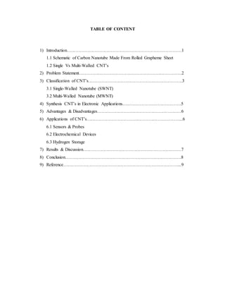
- 1. TABLE OF CONTENT 1) Introduction……………………………………………………………………1 1.1 Schematic of Carbon Nanotube Made From Rolled Grapheme Sheet 1.2 Single Vs Multi-Walled CNT’s 2) Problem Statement…………………………………………………………….2 3) Classification of CNT’s……………………………………………………….3 3.1 Single-Walled Nanotube (SWNT) 3.2 Multi-Walled Nanotube (MWNT) 4) Synthesis CNT’s in Electronic Applications………………………………….5 5) Advantages & Disadvantages…………………………………………………6 6) Applications of CNT’s………………………………………………………...6 6.1 Sensors & Probes 6.2 Electrochemical Devices 6.3 Hydrogen Storage 7) Results & Discussion………………………………………………………….7 8) Conclusion…………………………………………………………………….8 9) Reference……………………………………………………………………...9
- 2. INTRODUCTION Carbon nanotubes are first observed by Endo. This observed have lead to a great dal of scientific attention to unique material. Iijima’s detailed observations are make followed, caused theoretical models to start appear, predict unusual electronic properties for the class of material. At that time, carbon nanotube was predicted to be either metals or semiconductors based on their carbon atom’s arrangement. Carbon nanotubes (CNTs) is a tube-shaped material which made by carbon. It’s having a diameter measuring on the nanometer scale for which nanometer is one-billionth of a meter, or about 10,000 times smaller than a human hair. CNTs are unique with the strong bonding between atoms and ultimate aspect ratios in the tubes. CNTs can be as thin as a few manometer and be as long as hundreds of micron. CNTs have many structure, differing in length, thickness and number of layers. The characteristics of CNTs are depending on the graphene sheet. The way of graphene sheet rolled up to form the tube influence it to act metallic or as a semiconductor Schematic of carbon nanotube made from rolled grapheme sheet There are two category of CNTs which are single-walled (SWNT) or multi-walled nanotubes (MWNT). A single-walled carbon nanotube is shaped like a regular straw, only has 1 layer or wall. Multi-walled carbon nanotubes are a collection of nested tube with increasing diameters. Single vs multi-walled CNT Carbon Nanotubes (CNTs) exhibit uncommon electrical properties for organic materials. CNTs have a huge potential in electric and electronic application such as photovoltaic, sensors, semiconductor devices, displays, conductors, smart textiles and energy conversion devices. The type of CNT that is pf interest in the electronics industry is single-walled tube. The material is made from a carbon lattice that is one carbon atom thick. Carbon and silicon are both small size. The number of transistors made from CNTs that can be placed on a chip is much greater than the number that can be placed on a silicon chip. CNT chip are more faster, efficient and they generate much less heat than silicon chips. In other words, CNT chips would give high speed and longer battery life without overheating and need for fans to dissipate excess heat.
- 3. PROBLEM STATEMENT Since its discovery, carbon nanotubes or in other name is CNTs, has been very famous among electronics part industry. What is CNTs? What it do? CNTs is a tube-shaped materials that made up of carbon which its diameter is measuring by manometer scale. Through this, we can only imagine how small this CNTs and furthermore, it also bring lots of pros in this industry. CNTs have lots of usage in electronics industry such as flexible electronics, ultra-high sensitive sensors, high frequency electronics, opto-electronics and many more. CNTs have unique characteristics which is it have two states; metallic state and semiconducting state. It also can conduct high electricity. CNTs also have high tensile strength and also very flexible. Moreover, it can stretch up to 18% of elongation to failure. Plus, carbon nanotubes contain low thermal expansion coefficient and high thermal conductivity. It’s been said that CNTs’ unique characteristics making it the most favourable material when producing electronic parts such as transistor. But, a great invention also come with a problem. In this case, it comes up with two major problems which are the mixture problem and the electrical resistance problem. The first problem that come up is the mixture problem. As we know, carbon nanotubes are available in two state; metallic and semiconductor. Furthermore, integrated circuit using up to 100% of semiconductor. But the problem is, how to separate metallic CNTs from semiconductor? This problem is still on research by the scientist around the world. The second problem is the electrical problem. In electronic parts, the nanotubes will be connected with other metallic components. When the electricity flows through them, the electrical resistance will increase while the size of the connection is decreasing. The higher usage of CNTs will be results in increasing of resistance. This is because CNTs’ diameter is on scale of 10 nm or less.by increasing the size of the connection means less CNTs available in the electrical parts, thus making the advantage of the CNTs disappear.
- 4. CLASSIFICATION OF CNTs Carbon nanotubes which also called CNTs is make from graphite. The molecular structure of graphite resembles stacked. When grapheme are rolled into a cylinder with their edges joined, CNTs are formed. CNTs can have a variety of diameter, length, and functional group content. CNTs are divided into two type. A nanotube that consist of one tube of graphite, a one- atom thick is called single-walled nanotube while consist of a number of concentric tubes called multi-walled nanotubes. Single-walled Nanotube (SWNT) Most single-walled nanotubes (SWNTs) have a diameter of close to 1 nanometer, and can be extremely longer. The structure of a SWNT are form by wrapping a one-atom-thick layer of graphite called graphene into a seamless cylinder. The way the graphene sheet is wrapped is represented by a pair of indices (n.m). The integers n and m denote the number of unit vectors along two directions in the honeycomb crystal lattice of graphene. If m = 0, the nanotubes are called zigzag nanotubes, and if n = m, the nanotubes are called armchair nanotubes. Otherwise, they are called chiral. The diameter of an ideal nanotube can be calculated from its (n,m) indices as follows d = 𝑎 𝜋 √(𝑛2 + 𝑛𝑚 + 𝑛2 = 78.3√(( 𝑛 + 𝑚)2 − 𝑛𝑚) 𝑝𝑚, where a = 0.246 nm. Carbon nanotubes are predicted to be metallic or semiconducting due to diameter and the helicity of the arrangement of graphitic rings in walls. This prediction can be probe by Scanning Tunnelling Microscopy (STM). STM can resolve both atomic structure and the electronic density of states. Single-walled carbon nanotubes (SWNTs) have many exceptional electronic properties. SWNTs is an effective thin-film semiconductor that suitable for integration into transistors and others classes of electronic devices. The large number of SWNTs enable excellent device-level performance characteristics even with SWNTs are electronically heterogeneous. Measurements on p- and n-channel transistors involve as many as 2100 SWNTs reveal device-level mobility and scaled transconductance that approaching 1000 cm2 V−1 s−1 and 3000 S m−1, respectively, and with current outputs of up to 1 A in devices that use interdigitated electrodes. P-type metal-oxide-semiconductor logic, PMOS and Complementary Metal Oxide Semiconductor, CMOS logic gates and mechanically flexible transistors on plastic provide examples of devices that can be formed with this approach. Multi-Walled Nanotube (MWNT) Multi-walled nanotubes (MWNTs) consist of multiple rolled layers (concentric tubes) of graphene. Structures of MWNTs can be describe by two model which are Parchment model and Russian Doll model. In
- 5. the Parchment model, a single sheet of graphite is rolled in around itself, resembling a rolled newspaper. The interlayer distance in multi-walled nanotubes is close to the distance between graphene layers in graphite. In the Russian Doll model, sheets of graphite are arranged in concentric cylinders, for example small single- walled nanotube (SWNT) within a larger single-walled nanotube.. The Russian Doll structure is observed more commonly. Its individual shells can be described as SWNTs, which can be metallic or semiconducting. MWNT is usually a zero-gap metal due to the statistical probability and restrictions on the relative diameters of the individual tubes. Double-walled carbon nanotubes (DWNTs) form a special class of nanotubes because their properties are similar to SWNTs but their resistivity to chemicals are higher. This is important when it is necessary to graft chemical functions to the surface of the nanotubes (functionalization) to add properties to the CNT. Covalent functionalization of SWNTs will break some C=C double bonds, leaving "holes" in the structure on the nanotube, and thus modifying both its mechanical and electrical properties. In the case of DWNTs, only the outer wall is modified. DWNT synthesis on the gram- scale was first proposed in 2003 by the combustion chemical vapor deposition,CCVD technique, from the selective reduction of oxide solutions in methane and hydrogen. The telescopic motion ability of inner shells and their unique mechanical properties will permit the use of multi-walled nanotubes as main movable arms in coming nanomechanical devices. Retraction force that occurs to telescopic motion caused by the Lennard-Jones interaction between shells and its value is about 1.5 nN.
- 6. SYNTHESIS CNT’s IN ELECTRONIC APPLICATIONS 4.0 Synthesis CNT in Electronic Application 4.1 Synthesis of carbon nanotubes This was a significant disadvantage of the arc-discharge method for analysis on nanotubes, until 1997, when Journetand his co-workers found that the mixture 1 at.% Y and 4.2 at.% Ni as stimulus in graphite powder gave a high yield of 70-90% in their setup . Iijima first discovered the multiwall carbon nanotubes in 1991, when he worked on C60 and witnessed carbon soot on the negative graphite electrode produced in arc discharge shown in Figure 1. In 1992, Ebbesen and Ajayan effectuated growth and purification ofmultiwalled carbon nanotubes at the gram level using the arc-discharge method. In 1993, Iijima'sgroup , as well as Bethune and his associates found that the utilisation of transitional-metal stimulus in the arc-discharge process leads to nanotubes with only a single shell. Another highlight in the synthesis of single-walled carbon nanotubes is the effort made by Smalley's group in 1996. However, the yield of carbon nanotubes was low, and there were large amounts of metal carbide groups and indefinite shape carbon attached to the nanotubes. This method involves the condensation of carbon atoms and radicals from evaporation of solid carbon sources in arc discharge, and the temperature involved can be as high as 3000-4000 C. These nanotubes mostly have diameters around 5-30 nm and lengths around 10m. Figure 1. The transmission electron microscope (TEM) image of first discovered carbon nanotubes Iijima: the multiwalled carbon nanotubes he found in the soot of an arc-discharge setup. In spite of the success of the arc-discharge and laser ablation methods in producing carbon nanotubes with a high yield, the final products are usually bundled nanotubes decorated with stimulus particles and indefinite shape carbon. He and his co- workers at Rice University developed a laser ablation method that could grow single- walled carbon nanotubes with a single-walled carbon nanotubes with relatively high yield of more than 70%, which paved the way for the take-off of analysis on the physical properties of SWNTs. This method has been widely applied to remove indefinite shape carbon and excess catalytic metal particles commonly found mixed with nanotubes in the final product. They used the laser ablation on graphite rods doped with a mixture of cobalt and nickel powder in the environment followed by heat treatment in vacuum to remove C60 and other small fullerenes. Previous studies using such products have been critically constrained by the lack of control over the nanotube growth and the difficulty in wiring up individual
- 7. nanotube devices, making practical uses almost impossible. A purification process involving refluxing the as-grown nanotubes in a nitric acid for an extended period was also developed by Smalley and his co-workers. It is equally desirable to develop a method to make robust, low-resistance electrical contacts between nanotubes and metallic electrodes. Figure 2 shows the experiment setup and the bundled ropes generated by laser ablation would be desirable to have a high-yield generation route to produce SWNTs with controlled length, positions, and orientations for both scientific and technological studies. The nanotubes they got had highly uniform diameters and bundled together as "ropes" by van der Waals interaction. Figure 2. (a) The experimental setup of laser ablation method to synthesize the SWNT. The laser beam is focused on the carbon rod doped with catalysts when flowing inertial gas. The soot as the product is collected at the copper collector. Characteristic of carbon nanotubes can be different as it depending on how graphene sheet has rolled up to form the tube which can make it to become metallic or semiconductor. Carbon nanotubes can have many structures which diferent in length, thickness and number of layers. First, carbon nanotubes (CNts) are unique due to the bonding between the atoms is very strong. 1. Single-walled nanotubes (SWCNT) A single-walled nanotubes give a look of regular straw in shape. It only have one or single wall or layer which fold in to cylindrical shape. 2. multiple-walled nanotubes (MWCNT) The multi-walled nanotubes give a look of nested tubes of increasing in diameters. Its structure can be categorized into inner and outer tube and each tubes held some distance from each other by a strong interatomic forces. Figure 3. shows single and multi-walled CNTs From the beginning, carbon nanotubes are related to graphite. Carbon nanotubes are members of the fullerene structural. Graphine is a long, hollow structure with walls formed by one atom thick sheets of carbon. Figure 4. Schematic diagram of carbon nanotubes made from rolled graphine sheet. 4.2 Properties of carbon nanotubes
- 8. From the characteristic of carbon nanotubes above, we can know that the structure of CNTs can influence its properties which are electrical conductivity, thermal stability, density and so on. 4.2.1 Electronic Properties of carbon nanotubes However, unlike nanowires based on ordinary semiconductors, carbon nanotubes display rich electronic properties, the most important of which is that a carbon nanotube can be metallic, semi-metallic, or semiconducting, depending on its chirality and diameter [1, 38-42]. Band structure calculations have foreseen that armchair SWNTs with (n , n) indices are truly metallic with limited density of states at the Fermi level, whereas SWNTs with (m , n) indices are semiconducting when m - n ≠ 3 x integer and have first primary energy gaps Eg∝ 1/d, where d is the nanotube diameter SWNTs with (m, n) indices and m - n = 3 x integer are semi-metallic with zero band gap within tight-binding calculations based on pπ -orbitals alone. Research on the electronic transport through single walled carbon nanotubes went through enormous progress in the past few years. This has been mostly driven by the fascinating science and many potential usages related to nanotubes. Louie and co-workers have carried out first- principles ab initio calculations and found that the curvatures of small diameter SWNTs can lead to rehybridization of π∗- and σ∗- orbitals and thus manipulated electronic structures of SWNTs from those of flat graphene stripes. It was pointed out that the curvature of nanotubes leads to nonparallel π∗- orbitals interacting with σ∗- orbitals, which causes the opening of a small bandgap to result in an semiconductor from a semimetal. The following sections will review electronic transport studies on metallic, semi-metallic, and alsosemi- conducting nanotubes, with our focus on results obtained from nanotube devices generated via the CVD growth method. For SGS-SWNTs, the bandgaps depend on specific ( m - n ) indices and are in the range of 2-50 meV for d = 3-0.7 nm. 4.2.2 Carbon nanotube strength and elasticity The main atom in carbon nanotubes is carbon atom in single ( graphene) sheet of graphite form a planar lattice which have strong bonding to their another neighbouring atoms. From this, single-walled CNTs are stiffer than steel and have strong resistant to any huge physical outcome damage. The plane elastic modulus of graphite is one of the largest of any material due to this strong bonding. 4.2.3 Carbon nanotube thermal conductivity and expansion The almost zero in-plane thermal expansion but large inter-plane expansion of single- walled carbon nanotubes give a strong coupling and high flexibility against non- axial strain. CNTs have high thermal conductivity due to the strong in-plane graphite c-c bonds make them strong and stiffer against large strain. 4.2.4 Carbon nanotube high aspect ratio Their high aspect ratio imparts electrical conductivity at low loading when compared to carbon black, chopped carbon fiber. CNTs have high aspect ratio which low loading preserves more of the polymer resins especially at low temperatures. 4.3 Fabrication and overview of carbon nanotubes Making electrical contacts to individual carbon nanotubes lies at the heart of nanotube device production. A popular spin-on method was developed by McEuen and his co- workers, and Dekker and his co-workers. Asmall amount of carbon nanotube material, usually produced by laser ablation or arc discharge, is first disseminate into an organic solvent to form a suspension, and then spun onto a Si/SiO2 layer with predefined metal
- 9. electrodes. Besides, atomic force microscopy (AFM) is used to locate the nanotubes first and e-beam lithography is then carried out to define electrical contacts to the carbon nanotubes. In contrast, the controlled CVD method can directly grow individual carbon nanotubes at desired position on Si/ SiO2 layer [22-25], as described in Section 2, and therefore is superior in producing nanotube devices and integrated systems. This method is simple and easy to use however, it has no control over the nanotube location and alignment and the yield for good devices is usually low. AFM is usually employed to secure each device consists of a single nanotube bridging the metal electrodes. The electronic measurements are usually performed in the temperature range from 300 K downto 1.5 K and the heavily doped silicon layer is used to supply the gate bias. The length of the nanotubes between the electrodes is controlled by the e-beam lithography step and can change from 0.5 μm to 5 μm. The first category corresponds to nanotube devices with low resistance and weak or no gate dependence, generally regarded as the signature of metallic carbon nanotubes.The second category corresponds to devices with relatively low resistance; however, change in the gate bias can bring such devices from a conductive state to an almost insulating state, and then back to a conductive state.The third category corresponds to devices with high resistance and strong gate dependence, corresponding to semiconducting nanotubes.Most of the carbon nanotube devices fall into three categories according to their resistance and gate dependence.Such devices will be described in detail in Section 3.3 and are attributed to small-gap semiconducting (or semimetallic) carbon nanotubes. Figure 5. Bandgaps calculated for carbon nanotubes of various diameters.The tubes fall into three families: semiconducting nanotubes with primary gaps which scale as 1/R (top panel, top curve), semimetallicnanotubes with zero primary gap but nonzero curvature-induced gapswhich scale as 1/R2 (top panel, lower curve, and shown in the expanded scale in the lower panel), and armchair tubes with zero primary gapand zero curvature- induced gap Figure 6. Temperature-dependent resistance of a metallic SWNT. Inset: I-V and dI/dV−V curves recorded at 4 K.
- 10. 4.3.1 PURPOSE OF THE APPLICATION Due to their high conductivity, high aspect ratio, and natural tendency to form ropes, MWCNTs are ideal in providing inherently long conductive pathways even at ultra-low loadings. The lower loading of additive can offer several advantages such as better processability polymer. This is why the use of carbon nanotubes are well used for conductive and antistatic applications in sectors such as electronics and the automotive industry. Concrete examples in the automotive industry are fuel lines (connectors, pump parts, o-rings, and fuel systems components. Carbon fiber structural composites and a thermoset have been improved via development by the introduction of carbon nanotubes. Further more, CNT also plays important role in the electronic industry, conveyor belts, manufacturing tools and equipments, wafer carriers, clean room equipments. Every sports equipments on the market can be developed by using CNT. Professional athletes are more preferred to buy high-end models which includes the characteristic such as more durable and lighter weighted. For examples, the famous national Finnish ice hockey team is equipped with CNT reinforced sticks while Federer the tennis champion is playing with CNT reinforced rackets. These upcoming structural composite materials based on CNT reinforced thermoplastics or thermosets combine strong mechanical properties and low density and will direct a path to new developments. These will particularly replacing metals in various mechanical applications where a weight reduction could save energy, like in automotive industry. Carbon Nanotubes may also play a role in the modification of existing textile materials using electrostatic self-assembly and atomic layer deposition techniques to create novel and customizable surfaces on conventional textile materials with emphasis on natural fibres. For example, the improvement of mechanical properties in epoxy-glassfiber or epoxy–carbon fiber composites already known from the sport industry can also be used in the construction of light weighted composites for wind power generators and in the aircraft industry.
- 11. ADVANTAGES & DISADVANTAGES Advantages It is improves the conductive, mechanical and flame barrier properties of plastics and composites. It is resistant to temperature changes, meaning they function almost just as well in extreme cold as they do in extreme heat. Extremely small and lightweight. Resources required to produce are plentiful and many of them can be made with only a small amount of material. Disadvantages The components are extremely small, so are difficult to work with. The process to produce the carbon nanotubes is quite expensive. In the research, most of the scientists still do not understand exactly how they work.
- 12. APPLICATIONS Sensors and Probes In this research, chemical sensor applications of non-metallic nanotubes are interesting because of nanotube electronic transport and also thermos power which is voltages between junctions caused by inter- junction temperature differences that are very sensitive to substances that affect the amount of injected charge. The mechanical robustness of the nanotubes and the low buckling forces dramatically increase probe life and minimize the sample of damage during repeated hard crashes into substrates. The cylindrical shape and small tube diameter enable imaging in narrow, deep crevices and improve resolution in comparison to conventional nanoprobes, especially for high sample feature heights. Nanoscopic tweezers have been made that are driven by the electrostatic interaction between two nanotubes on a probe tip. Electrochemical Devices Electronical devices is the high electrochemically accessible surface area of porous nanotube arrays, which combined with their high electronic conductivity and it is useful mechanical properties, these materials are attractive as electrodes for devices that use electrochemical double- layer charge injection. For examples, “supercapacitors” which have giant capacitances in comparison with those of ordinary dielectric-based capacitors, and electromechanical actuators that may eventually be used in robots. Like the others capacitors, carbon nanotube supercapacitors and electromechanical actuators actually comprise two electrodes separated by an electronically insulating material, which is ionically conducting in electrochemical devices. The capacitance for an electrochemically device depends on the separation between the charge on the electrode and the countercharge in the electrolyte. When the separation is about a nanometer for nanotubes in electrodes, as compared with the micrometer or larger separations in ordinary dielectric capacitors, very large capacitances result from the high nanotube surface area accessible to the electrolyte. The use of nanotubes as electrodes in lithium batteries is a possibility because of the high reversible component of storage capacity at high discharge rates. The maximum reported reversible capacity is 1000mA-hour/g for graphite and 708 mA- hour/g for ball-milled graphite. However, the large irreversible component to capacity (coexisting with the large reversible storage capacity), an absence of a voltage plateau during discharge, and the large hysteresis in voltage between charge and discharge currently limit energy storage density and energy efficiency, as compared with those of other competing materials. Hydrogen Storage Carbon nanotube have the potentially useful for hydrogen storage. For example, for fuel cells that power electric vehicles. However, experimental reports of high storage capacities reported that it is impossible to access the applications potential.
- 13. RESULTS & DISCUSSIONS 5.0 Discussion Carbon nanotubes are an extraordinary bit of innovation, and new uses for them are being found each day. Be that as it may they do have their downsides.The disadvantages of carbon nanotubes are : i.Regardless of all the exploration, researchers still don't see precisely how they function ii.Extremely little, so are hard to work with iii.Currently, the procedure is moderately costly to create the nanotubes iv.Would be costly to execute this new innovation in and supplant the more established innovation in every one of the spots that we could v.At the rate our innovation has been getting to be plainly out of date, it might be a bet to wager on this innovation Carbon nanotubes (CNTS) have unique properties as they are quasi-one-dimension materials and are ideal materials for application in electronic devices. The main reason for choosing carbon nanotubes as the role material in electronic devices is that the carbon atoms in carbon nanotubes are strongly and firmly connected. Each atom has three bonds to the other atoms, and all these bonds are covalent bond
- 14. CONCLUSION So in conclusion, carbon nanotubes bring lots of benefits to mankind. Its discovery was a miracle and also revolutionize today’s electronic parts. As we know, carbon nanotubes have unique characteristics. These characteristics make it so special, even other material cannot compete with it. Carbon nanotubes are used in many ways like sensors and probes, electrochemical device and hydrogen storage. Carbon nanotubes can be classified into two part; single-walled nanotubes and multi-walled nanotubes. Moreover, the properties that shape up the CNTs are its electronic properties, which is it consist of metallic and semiconductor, its strength and elasticity, where the CNTs is durable and consist of high strength, its thermal conductivity and expansion and lastly its high aspect ratio. But despites its greatness, everything have its pros and cons. For carbon nanotubes, it has more pros than cons such as small and lightweight. But to produce these nanotubes, it need higher cost. Thus, making a part using CNTs is very expensive and costly. After synthesizing the true meaning of carbon nanotubes and its function, we can conclude that CNTs is one of the greatest discovery and also bring lots of improvement in electronic parts.
- 15. REFERENCE Oberlin, M. Endo, T. Koyama, J. of Crystal Growth 32, 335 (1976). M. Endo, Chem Tech 18, 568 (1988). S. Iijima, Nature 354, 56 (1991). R. Saito, G. Dresselhaus, M. S. Dresselhaus, Physical Review B (Condensed Matter) 0, 14698 (1994). N. Hamada, S. Sawada, A. Oshiyama, Phys. Rev. Lett. 68, 1579 (1992). Nanotechnology: Basic Science and Emerging Technologies", M. Wilson et al, (2002) EC 2010 Engineered Nanoparticles: Review of Health and Environmental Safety (ENRHES). Project final report http://ihcp.jrc.ec.europa.eu/whats -new/enhres-final-report NIOSH 2010 NIOSH Current Intelligence Bulletin, Occupational Exposure to Carbon Nanotubes and Nanofibers (November 2010 Draft) http://www.cdc.gov/niosh/docket /review/docket161A/default.html Nakanishi J (ed) 2011 Risk Assessment of Manufactured Nanomaterials: Carbon Nanotubes. Final report issued on 17 August 2011 NEDO project (P06041) "Research and Development of Nanoparticle Characterization Methods" http://www.aist- riss.jp/main/modules/product/nan o_rad.html?ml_lang=en