
Recommended
More Related Content
What's hot
What's hot (20)
Similar to Chapter7
Similar to Chapter7 (20)
Recently uploaded
Recently uploaded (20)
Chapter7
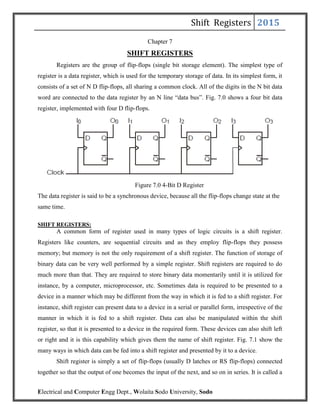
- 1. Shift Registers 2015 Electrical and Computer Engg Dept., Wolaita Sodo University, Sodo Chapter 7 SHIFT REGISTERS Registers are the group of flip-flops (single bit storage element). The simplest type of register is a data register, which is used for the temporary storage of data. In its simplest form, it consists of a set of N D flip-flops, all sharing a common clock. All of the digits in the N bit data word are connected to the data register by an N line “data bus”. Fig. 7.0 shows a four bit data register, implemented with four D flip-flops. Figure 7.0 4-Bit D Register The data register is said to be a synchronous device, because all the flip-flops change state at the same time. SHIFT REGISTERS: A common form of register used in many types of logic circuits is a shift register. Registers like counters, are sequential circuits and as they employ flip-flops they possess memory; but memory is not the only requirement of a shift register. The function of storage of binary data can be very well performed by a simple register. Shift registers are required to do much more than that. They are required to store binary data momentarily until it is utilized for instance, by a computer, microprocessor, etc. Sometimes data is required to be presented to a device in a manner which may be different from the way in which it is fed to a shift register. For instance, shift register can present data to a device in a serial or parallel form, irrespective of the manner in which it is fed to a shift register. Data can also be manipulated within the shift register, so that it is presented to a device in the required form. These devices can also shift left or right and it is this capability which gives them the name of shift register. Fig. 7.1 show the many ways in which data can be fed into a shift register and presented by it to a device. Shift register is simply a set of flip-flops (usually D latches or RS flip-flops) connected together so that the output of one becomes the input of the next, and so on in series. It is called a
- 2. Shift Registers 2015 Electrical and Computer Engg Dept., Wolaita Sodo University, Sodo shift register because the data is shifted through the register by one bit position on each clock pulse. Fig. 7.2 shows a four bit shift register, implemented with D flip-flops. Figure 7.2 4-bit Serial-in Serial-out Shift Register 7.1. Operation of the Shift Register: A 4-bit shift register constructed with D type flip-flop (Fig. 7.2) and JK flip-flop. By addition or deletion of flip-flop more or fewer bits can be accommodated. Except for FF0, the logic level at a data input terminal is determined by the state of the preceding flip-flop. Thus, Dn is 0 if the preceding flip-flop is in the reset state with Qn–1 = 0, and Dn = 1 if Qn–1 = 1. The input at FF0 is determined by an external source. From the characteristic of D-flip-flop we know that immediately after the triggering transition of the clock, the output Q of flip-flop goes to the state present at its input D just before this clock transition. Therefore, at each clock transition, pattern of bits, 1s and 0s, is shifted one flip-flop to the right. The bit of the last flip-flop (FF3 in Fig. 7.3) is lost, while the first flip-flop (FF0) goes to the state determined by its input D0. This operation is shown in Fig. 7.3. We have assumed that the flip-flop triggers on the positive-going transition of the clock waveform, and initially we have D0 = 0, FF0 = 1 and FF2 = FF3 = FF4 = 0. Figure 7.3 A 4-bit shift Register Operation
- 3. Shift Registers 2015 Electrical and Computer Engg Dept., Wolaita Sodo University, Sodo 7.2. Types of Shift Registers The basic modes of operation of shift registers such as Serial In- Serial Out, Serial In- Parallel Out, Parallel In-Serial Out, Parallel In-Parallel Out, and bidirectional shift registers. 7.2.1 Serial In–Serial Out Shift Registers A basic four-bit shift register can be constructed using four D-flip-flops, as shown in Fig. 7.4. The operation of the circuit is as follows. The register is first cleared, forcing all four outputs to zero. The input data is then applied sequentially to the D input of the first flip-flop on the left (FF0). During each clock pulse, one bit is transmitted from left to right. Assume a data word to be 1001. The least significant bit of the data has to be shifted through the register from FF0 to FF3. Figure 7.4 A 4-bit Shift Register using D-Flip flops In order to get the data out of the register, they must be shifted out serially. This can be done destructively or non-destructively. For destructive readout, the original data is lost and at the end of the read cycle, all flip-flops are reset to zero. To avoid the loss of data, an arrangement for a non-destructive reading can be done by adding two AND gates, an OR gate and an inverter to the system. The construction of this circuit is shown in Fig. 7.5 The data is loaded to the register when the control line is HIGH (i.e. WRITE). The data can be shifted out of the register when the control line is LOW (i.e. READ).
- 4. Shift Registers 2015 Electrical and Computer Engg Dept., Wolaita Sodo University, Sodo Figure 7.5 AND-OR Inverter system 7.2.2 Serial In-Parallel out Shift Registers The data bits are entered serially in the same manner as discussed in the last section. The difference is the way in which the data bits are taken out of the register. Once the data are stored, each bit appears on its respective output line, and all bits are available simultaneously. A construction of a four-bit serial in-parallel out register is shown in Fig. 7.6. Figure 7.6 A 4-bit SIPO register 7.2.3 Parallel In-Serial out Shift Registers A four-bit parallel in-serial out shift register is shown in Fig. 7.7. The circuit uses D-flip- flops and NAND gates for entering data (i.e., writing) to the register. D0, D1, D2 and D3 are the parallel inputs, where D0 is the most significant bit and D3 is the least significant bit. To write data in, the mode control line is taken to LOW and the data is clocked in. The data can be shifted when the mode control line is HIGH as SHIFT is active high. The register performs right shift operation on the application of a clock pulse. Figure 7.7 A PISO Register
- 5. Shift Registers 2015 Electrical and Computer Engg Dept., Wolaita Sodo University, Sodo 7.2.4 Parallel In-Parallel Out Shift Registers For parallel in-parallel out shift registers, all data bits appear on the parallel outputs immediately following the simultaneous entry of the data bits. The following circuit is a four bit parallel in-parallel out shift register constructed by D-flip-flops. Figure 7.8 A PIPO Register The D’s are the parallel inputs and the Q’s are the parallel outputs. Once the register is clocked, all the data at the D inputs appear at the corresponding Q outputs simultaneously. 7.2.5 Bidirectional Shift Registers (Universal Shift Register) The registers discussed so far involved only right shift operations. Each right shift operation has the effect of successively dividing the binary number by two. If the operation is reversed (left shift), this has the effect of multiplying the number by two. With suitable gating arrangement a serial shift register can perform both operations. Figure 7.9 Bidirectional Shift Register
- 6. Shift Registers 2015 Electrical and Computer Engg Dept., Wolaita Sodo University, Sodo A bi-directional, or reversible shift register is one in which the data can be shift either left or right. A four-bit bi-directional shift register using D-flip-flops is shown in Fig. 7.9. Here a set of NAND gates are configured as OR gates to select data inputs from the right or left adjacent bistables, as selected by the LEFT/RIGHT control line. 7.3 APPLICATIONS OF SHIFT REGISTERS Shift registers can be found in many applications. Here is a list of a few. 7.3.1 To Produce Time Delay The serial in-serial out shift register can be used as a time delay device. The amount of delay can be controlled by: the number of stages in the register (N) the clock frequency (f) The time delay ΔT is given by ∆T = N* f 7.3.2 To Simplify Combinational Logic The ring counter technique can be effectively utilized to implement synchronous sequential circuits. A major problem in the realization of sequential circuits is the assignment of binary codes to the internal states of the circuit in order to reduce the complexity of circuits required. By assigning one flip-flop to one internal state, it is possible to simplify the combinational logic required to realize the complete sequential circuit. When the circuit is in a particular state, the flip-flop corresponding to that state is set to HIGH and all other flip-flops remain LOW. 7.3.3 To Convert Serial Data to Parallel Data A computer or microprocessor-based system commonly requires incoming data to be in parallel format. But frequently, these systems must communicate with external devices that send or receive serial data. So, serial-to-parallel conversion is required. As shown in the previous sections, a serial in-parallel out register can achieve this. 7.4. Shift Register Counters Two of the most common types of shift register counters are introduced here: the Ring counter and the Johnson counter. They are basically shift registers with the serial outputs connected back to the serial inputs in order to produce particular sequences. These registers are classified as counters because they exhibit a specified sequence of states.
- 7. Shift Registers 2015 Electrical and Computer Engg Dept., Wolaita Sodo University, Sodo Ring Counters A ring counter is basically a circulating shift register in which the output of the most significant stage is fed back to the input of the least significant stage. The following is a 4-bit ring counter constructed from D flip-flops. The output of each stage is shifted into the next stage on the positive edge of a clock pulse. If the CLEAR signal is high, all the flip-flops except the first one FF0 are reset to 0. FF0 is preset to 1 instead. Since the count sequence has 4 distinct states, the counter can be considered as a mod-4 counter. Only 4 of the maximum 16 states are used, making ring counters very inefficient in terms of state usage. But the major advantage of a ring counter over a binary counter is that it is self-decoding. No extra decoding circuit is needed to determine what state the counter is in. Johnson Counters
- 8. Shift Registers 2015 Electrical and Computer Engg Dept., Wolaita Sodo University, Sodo Johnson counters are a variation of standard ring counters, with the inverted output of the last stage fed back to the input of the first stage. They are also known as twisted ring counters. An n-stage Johnson counter yields a count sequence of length 2n, so it may be considered to be amod-2n counter. The circuit above shows a 4-bit Johnson counter. The state sequence for the counter is given in the table as well as the animation on the left. Again, the apparent disadvantage of this counter is that the maximum available states are not fully utilized. Only eight of the sixteen states are being used. Beware that for both the Ring and the Johnson counter must initially be forced into a valid state in the count sequence because they operate on a subset of the available number of states. Otherwise, the ideal sequence will not be followed. Applications Shift registers can be found in many applications. Here is a list of a few. To produce time delay The serial in -serial out shift register can be used as a time delay device. The amount of delay can be controlled by: 1. the number of stages in the register 2. the clock frequency To simplify combinational logic The ring counter technique can be effectively utilized to implement synchronous sequential circuits. A major problem in the realization of sequential circuits is the assignment of binary codes to the internal states of the circuit in order to reduce the complexity of circuits required. By assigning one flip-flop to one internal state, it is possible to simplify the combinational logic required to realize the complete sequential circuit. When the circuit is in a particular state, the flip-flop corresponding to that state is set to HIGH and all other flip-flops remain LOW.
- 9. Shift Registers 2015 Electrical and Computer Engg Dept., Wolaita Sodo University, Sodo To convert serial data to parallel data A computer or microprocessor-based system commonly requires incoming data to be in parallel format. But frequently, these systems must communicate with external devices that send or receive serial data. So, serial-to-parallel conversion is required. As shown in the previous sections, a serial in - parallel out register can achieve this.
- 10. Shift Registers 2015 Electrical and Computer Engg Dept., Wolaita Sodo University, Sodo QUESTION BANK 1. Define shift register. Draw and explain 4 bit serial in parallel out shift register 2. Explain a 4-bit serial input shift registers in detail and give its timing diagram 3. Explain the different types of registers with relevant circuit diagrams 4. Name and explain in short the four basic types of shift registers and draw the block diagram for each 5. Explain any two shift registers with waveforms? 6. Draw the logic diagram of 4 bit Serial In Serial out shift register using JK flip-flop and explain its working with an example 7. Write a short notes on 4 bit bi-directional shift register with parallel load capabilities 8. With diagram explain universal shift register 9. State various applications of shift registers briefly 10. Explain the working of PIPO register with circuit