1. Analysis and Applications of the Capacitive Transformer
Ramon Vargas Patron
rvargas@inictel.gob.pe
INICTEL-UNI
Wide-band impedance-transformation techniques make common use of magnetic- coupling devices such as transformers (or autotransformers) and baluns for energy transfer between sections of a circuit. Engineering solutions in this area have been well documented in the past and are readily available to the circuit designer from dedicated technical sources.
When operation in a narrow band of frequencies is desired, the engineer usually resorts to a number of passive reactive networks exhibiting impedance-transformation properties. One example is the capacitive transformer, which has received extensive use since the very early days of radio. Surprisingly, however, technical information regarding its operation principle and application data is scarce in the currently available literature. Hence, design work involving this specific network alternatively uses time- consuming trial-and-error methods.
It is the purpose of this article to present a comprehensive analysis of the capacitive transformer and to illustrate how derived results can be incorporated into the design of a simple RF matching network and a grounded-base AF Colpitts oscillator.
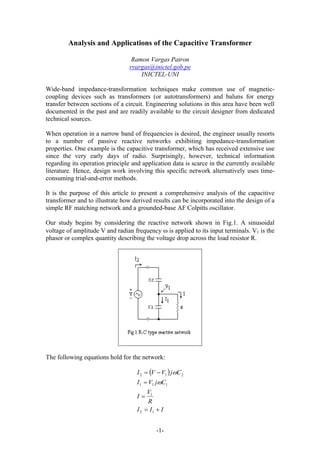
Our study begins by considering the reactive network shown in Fig.1. A sinusoidal voltage of amplitude V and radian frequency ω is applied to its input terminals. V1 is the phasor or complex quantity describing the voltage drop across the load resistor R.
The following equations hold for the network:
() IIIRVICjVICjVVI+= = = −= 121111212 ωω
-1-
2. Combining the above equations gives:
() RVCjVCjVV11121+=−ωω
Then:
() RVCjCjVCVj12112++=ωωω ()⎥⎦ ⎤ ⎢⎣ ⎡++=2111CCjRVω () ⎥⎦ ⎤ ⎢⎣ ⎡++ = RRCCjV2111ω
Solving for V1 yields: ( )R CCjRCjVV21211++ = ωω …(1)
From the set of basic equations for the network and Eq.(1) we obtain:
()221221CjRCCjRCjVVIωωω ⎥⎦ ⎤ ⎢⎣ ⎡ ++ −= ()221111CjRCCjRCjVωωω ⎥⎦ ⎤ ⎢⎣ ⎡ ++ + =
Input admittance is: ()2211211CjRCCjRCjVIωωω ⎥⎦ ⎤ ⎢⎣ ⎡ ++ + = ()()[] ()222212211111CjRCCRCCjRCjωωωω ++ +−+ = ()( ()
)
2222122121212111CjRCCCCRCRCjRCCjωωωωω ++ ++++− = () ()22221221212211CjRCCRCCCRCjωωωω ++ ++− = ()[] ()2221222112222211RCCRCCCCjRC++ +++ = ωωωω …(2)
-2-
3. If ω2(C1+C2)2R2>>1, then: () ()[] ()22212211222212221RCCRCCCjCRCCCVI+ ++ + + ≅ ωω
If also ω2C1(C1+C2)R2>>1: ()2121221222CCCCjRCCCVI+ + + ≅ω …(3)
Eq.(3) suggests the equivalent network depicted in Fig.2, as seen from the source side, where: RCCCRT2221⎟⎟⎠ ⎞ ⎜⎜⎝ ⎛+ = …(3.1) RCC2211⎟⎟⎠ ⎞ ⎜⎜⎝ ⎛ +=
and 2121CCCCC+ = …(3.2)
It is interesting to observe that Eq.(1) reduces to: 2121CCCVV+ = …(3.3)
indicating that the voltage drop across the load resistor is in phase with the applied source voltage and smaller by a fraction C2/(C1+C2) . Another equivalent network may be drawn as indicated by Fig.3. Clearly, the R-C network can be made to act as an ideal transformer paralleled by a capacitance C at the primary side, with the resistive load R connected to the secondary circuit and having a 1:n turns-ratio, where:
-3-
4. 212CCCn+ = …(3.4)
The original R-C network will be referred to hereafter as the capacitive transformer.
We shall now define the following: RG1= …(4.1) ()RCCQE21+=ω …(4.2) TRGn12= …(4.3) GnCQT2 ω = …(4.4)
Expressions (4.3) and (4.4) give, respectively, the input conductance and the “Q” at the input port when QE2 >>1. For this case, the relationship between QT and QE is: ⎟⎠ ⎞ ⎜⎝ ⎛− = nnQQET1 …(4.5)
From Eq.(2), a more general expression for input conductance can be obtained: ()222122221RCCRCGeq++ = ωω …(5)
Using set of definitions (4), we arrive to an equivalent form for Geq: 22221EeqQRCG+ = ω () 2221221EQRCCn+ + = ω
-4-
5. RQQnGEEeq11222⋅ + = 2221EEQQGn+ ⋅= …(5.1)
Input conductance is then:
…(5.2) GnGeqeq2=
where: 22221EEeqQQnn+ = …(5.3)
When QE2 is large, the input conductance is approximated by n2G.
Next, we shall compute the percentage error Δ1 when n2G is used for the input conductance instead of the exact value neq2G. %10021⎟⎟ ⎠ ⎞ ⎜⎜ ⎝ ⎛− ×=ΔeqeqGGGn % 111002222222⎟⎟⎟⎟⎟ ⎠ ⎞ ⎜⎜⎜⎜⎜ ⎝ ⎛ + + − ×= EEEEQQGnQQGnGn%1002⎟⎟ ⎠ ⎞ ⎜⎜ ⎝ ⎛ = EQ
If QE is made equal to 10, the percentage error is 1%. So, Geq = n2G within 1% when QE = 10.
Eq.(2) also gives the equivalent input susceptance Beq for the more general case: ()[] ()2221222112211RCCRCCCCBeq++ ++ = ωωω …(6)
which corresponds to a capacitance: ()[] ()2221222112211RCCRCCCCCeq++ ++ = ωω …(6.1)
-5-
6. or equivalently: ()[] 222111EEeqQQnCC+ −+ = …(6.2)
If QE2 is large, the equivalent input capacitance is C = C1C2/(C1+C2).
Let´s compute now the percentage error Δ2 when using C for the equivalent input capacitance instead of the exact value Ceq. %1002⎟⎟ ⎠ ⎞ ⎜⎜ ⎝ ⎛− ×=ΔeqeqCCC ()[] ()[]% 1111111002222222121⎥⎥⎥⎥⎥ ⎦ ⎤ ⎢⎢⎢⎢⎢ ⎣ ⎡ + −+ + −+ − + ×= EEEEQQnCQQnCCCCC ()()()[] ()% 111111100222⎥⎦ ⎤ ⎢⎣ ⎡ −+ −+−+− ×= EEEQnQnQn ()% 111002⎟⎟ ⎠ ⎞ ⎜⎜ ⎝ ⎛ −+ −= EQnn
In most practical cases it reduces to: % 12⎟⎠⎞ ⎜⎝ ⎛ − −=Δnn
when QE = 10.
Two examples will follow showing practical application for the derived formulae.
Design of an RF matching network
It is desired to transform a 50-ohm resistive load into a 5k-ohm value at a frequency of 10MHz using a capacitive transformer. The required values for C1 and C2 can be readily calculated as follows.
First, we choose QE = 10. Then, knowing that ω = 2π x 107 Rad/sec and R = 50 ohms, from (4.2) we obtain: nFCC18.35010210721= ××=+ π
-6-
7. Next, from Eq.(3.4) and given data: 1.0500050212== + = CCCn
Then:
nFnFnFCnFnFC862.2318.018.3318.018.31.012=−= =×=
The input capacitance is: pFnFnFCCCCC2.2862862.018.3318.0862.22121== ×= + =
with a –0.11% error. The “Q” at the input port is given by Eq.(4.5): 901=⎟⎠ ⎞ ⎜⎝ ⎛− = nnQQET
Fig.4 below depicts the capacitive transformer that will effect the required impedance transformation.
The capacitance C = 286.2pF can be tuned out at 10MHz by an inductance L = 0.885uH.
Design of a grounded-base AF Colpitts oscillator
Sine-wave oscillator configurations basically differ from each other in the way signal voltages (or currents) are fed back from the output port to the input, while loop gain is maintained slightly above unity. The Colpitts oscillator, for example, operates successfully thanks to the correct capacitive tapping of the signal voltage existing
-7-
8. across the L-C tuning tank. It constitutes an excellent example of application of the capacitive transformer in an oscillator circuit.
Fig.5 below shows the schematic diagram of a 1kHz grounded-base Colpitts oscillator that was chosen for a proof-of-concept implementation. The inductance L of the tank circuit was provided by a pair of 2k ohms DC-resistance high-impedance magnetic headphones, which doubled as a hearing device. The headphones as measured on a B&K Precision 875A LCR Meter gave L = 1.32H (series inductance) and r = 2k ohms (series resistance), at 1kHz. The power supply was selected to be 3V DC and the quiescent emitter current was set to 0.62mA, for best collector-voltage swing.
Following, loop-gain calculations will be made for the oscillator, identifying capacitive transformer-like operation. C1 and C2 will then be computed with the help of previously derived formulae.
The small-signal equivalent model for loop-gain calculation is shown in Fig.6, where: mhoshmAIgibEmQ0248.032.401125)( ====
and: HQLLS39.1112'=⎟⎟ ⎠ ⎞ ⎜⎜ ⎝ ⎛ +=
()kohmsQrRSP39.3612=+= 147.4200032.11023= ××== πω rLQoscS
-8-
9. L’ and RP are calculated using the known series-to-parallel impedance transformation pair. If we refer to the parallel combination of Re and hib as R, it is not difficult to identify a capacitive transformer-like action due to C2 , R and C1.
Loop gain at the oscillation frequency is given by (please refer to Appendix for proof): ()221// 'EEeqPmebbeQQnRRgvv+ ⋅=
using capacitive-transformer terminology. If Req = 1/Geq >>RP, then: min2211nQQgRnEEmP= + ⋅≥
for oscillations to be sustained. The capacitive transformer comprising C1, C2, Re and hib imposes an equivalent capacitance:
()[] 222111EEeqQQnCC+ −+ =
across L’. The oscillation frequency ωosc = 2πfosc is given in the Appendix as: ⎟⎟⎠ ⎞ ⎜⎜⎝ ⎛ += INEeqoscQQCL111' 2ω
where: 'LRQoscPINω =
-9-
10. The design procedure for the oscillator simplifies if we select: 1212<< + = CCCn
which readily makes . Thus, we may write: 2CCeq≈ nCCCeq=+21 nRCQeqoscE ω =
and:
() nCnCeq− = 11
The design steps for our grounded-base Colpitts oscillator will be then:
1. Choose QE such that nmin<<1. This will make 2CCeq≈.
2. Obtain C2 from the expression for ωosc.
3. From that for QE obtain the value of n. Check that n>nmin.
4. Compute C1.
Applying the above procedure to our 1kHz oscillator:
1. We select QE = 1 to obtain nmin = 0.0022 << 1.
2. For this value of QE, and knowing that 17.439.11021039.3633= ×××= πINQ, we get: nFCCeq59.222=≈
3. Knowing that R = Re//hib = 37.78 ohms, we obtain: min00536.0nQRCnEeqosc>== ω
4. C1 is computed from () uFCCnCnCeqeqeq19.457.18500536.000536.0111== − = − =
-10-
11. APPENDIX
The grounded-base Colpitts oscillator may be modelled as depicted in the figure below, where H(jω) is a functional block equivalent to Eq.(1) from the previous section:
() EEjQjnQVVjH+ == 11ω
If Req>>RP, loop gain will be expressed by: ()⎟⎟⎠ ⎞ ⎜⎜⎝ ⎛ + − ⋅ +− − =⋅= EEPeqmbeebebbejQjnQRLjCLLjgvvvvvv11' '2' ''ωωω () PEPEeqEEmRQLRLjjQCLjQnQLg'' '2' 11 ωωωω −++−+ − = ⎟⎟⎠ ⎞ ⎜⎜⎝ ⎛ −++⎟⎟⎠ ⎞ ⎜⎜⎝ ⎛ −− − = EeqPEPEeqEmQCLRLQjRQLCLnQLg'2'' '2' 1ωωωωω
For oscillations to occur: 01' jvvebbe+=
-11-
12. Then: 0'2' =−+EeqPEQCLRLQωω
or: INEeqoscQQCL11'2+=ω
where 'LRQoscPINω =. In a much more familiar form: ⎟⎟⎠ ⎞ ⎜⎜⎝ ⎛ += INEeqoscQQCL111' 2ω …(A-1)
which gives the frequency of the oscillation oscoscfπω2=.
Loop gain remains as: PEosceqoscEoscmebbeRQLCLnQLgvv' '2' 1'ωωω +− = INEINEEoscmQQQQnQLg+ = 1'ω 221EEPmQQnRg+ =
For sustained oscillations: 1122≥ +EEPmQQnRg
Then: min2211nRgQQnPmEE=⋅ + ≥ …(A-2)
-12-
13. The condition Req>>RP implies: () PEEeqeqRQnQRnRR>> + ==22221 …(A-3)
or: PEERRQQn⋅ + <<2221 …(A-4)
which imposes an upper limit on n.
In the more general case, the condition for oscillation may be shown to be: ()11//22≥ +EEeqPmQQRRng …(A-5)
which requires solving a second-degree algebraic equation for n, due to the relationship existing between Req and this variable, as stated by Eq. (A-3) above.
Ramon Vargas Patron rvargas@inictel.gob.pe
Lima-Peru, South America
February 11th 2007
-13-

![Combining the above equations gives:
() RVCjVCjVV11121+=−ωω
Then:
() RVCjCjVCVj12112++=ωωω ()⎥⎦ ⎤ ⎢⎣ ⎡++=2111CCjRVω () ⎥⎦ ⎤ ⎢⎣ ⎡++ = RRCCjV2111ω
Solving for V1 yields: ( )R CCjRCjVV21211++ = ωω …(1)
From the set of basic equations for the network and Eq.(1) we obtain:
()221221CjRCCjRCjVVIωωω ⎥⎦ ⎤ ⎢⎣ ⎡ ++ −= ()221111CjRCCjRCjVωωω ⎥⎦ ⎤ ⎢⎣ ⎡ ++ + =
Input admittance is: ()2211211CjRCCjRCjVIωωω ⎥⎦ ⎤ ⎢⎣ ⎡ ++ + = ()()[] ()222212211111CjRCCRCCjRCjωωωω ++ +−+ = ()( ()
)
2222122121212111CjRCCCCRCRCjRCCjωωωωω ++ ++++− = () ()22221221212211CjRCCRCCCRCjωωωω ++ ++− = ()[] ()2221222112222211RCCRCCCCjRC++ +++ = ωωωω …(2)
-2-](data:image/gif;base64,R0lGODlhAQABAIAAAAAAAP///yH5BAEAAAAALAAAAAABAAEAAAIBRAA7)