Microsystems Technologies Thin Film Processes Guide
•
2 likes•751 views

This document discusses various thin film processing techniques used in microsystems technologies. It covers topics such as microfabrication techniques including photolithography, etching, and bonding. It also discusses additive thin film deposition methods like oxidation, chemical vapor deposition, physical vapor deposition, sputtering and evaporation. Subtractive thin film processes like wet and dry etching of materials are also covered. Sacrificial layer processes, electrodeposition, electroforming and other inorganic material processes are summarized as well.

Recommended
More Related Content
What's hot
What's hot (19)
Similar to Microsystems Technologies Thin Film Processes Guide
Similar to Microsystems Technologies Thin Film Processes Guide (20)
Recently uploaded
Recently uploaded (20)
Microsystems Technologies Thin Film Processes Guide
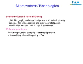
- 1. Microsystems Technologies Selected traditional micromachining photolithography and mask design, wet and dry bulk etching, bonding, thin film deposition and removal, metallization, sacrificial processes, other inorganic processes Polymer techniques thick-film polymers, stamping, soft lithography and micromolding, stereolithography, LIGA
- 2. Thin-Film Processing: Introduction Subtractive processes Wet etching insulators metals insulators metals Additive processes Oxidation of silicon Chemical vapor depostion (CVD) LPCVD/PECVD oxide, nitride, polysilicon epitaxy Physical vapour deposition sputtering evaporation Physical deposition: spin-on-glass other spin-on Combined processes Sacrificial processes Example uses of thin film processes in bio-microsystems Masking Channel fabrication and coating Metal electrodes, routing Active films for actuation (valves,pumps) Sealing Doping ion implantation diffusion We will only look at a few most relevant ones. Dry etching
- 3. Thin-Film Processing:Additive Processes Oxidation of Silicon “Bare” silicon “always” has ~15-20 Å of “native” SiO2 Two types: wet and dry oxidation Dryoxidation Wetoxidation Si + O2 SiO2 Si + 2H2O SiO2 + 2H2 Wet oxidation is faster, but dry oxidation gives a more dense film Addition of boron or phosphorous: borosilicate glass (BSG) phosphosilicate glass (PSG) Uses: etch mask Both processes consume silicon! surface passivation insulation and isolation (e.g., under electrodes) microelectronics uses (e.g., gate oxide)
- 4. Thin-Film Processing: Additive Processes Oxidation growth over time Dry oxidation Wet oxidation Provided for your reference only, although note practical times, thicknesses, and use of high temperatures!
- 5. Thin-Film Processing:Additive Processes Chemical vapor deposition: CVD Formation of film on substrate by reaction of vapor phase chemicals;the higher the temp ೦the higher the deposition rate Typically deposited materials: silicon dioxide (including low-temp, or LTO), doped for PSG, BSG, and PBSG silicon nitride poly and amorphous silicon silicon carbide metal
- 6. Thin-Film Processing:Additive Processes CVD steps 1. 2. 3. 4. 5. Gases are introduced into reaction chamber Gas species are moved to substrate Reactants are adsorbed onto the surface Film-forming chemical reactions Desorption and removal of by-products
- 7. Thin-Film Processing: CVD CVD: film quality issues 1. Stoichiometery: exact composition of the film 2. Purity of film and contamination, 3. particulatesUniformity and thickness 4. Conformality and step coverage 5. Pin holes and cracks 6. Adhesion of film 7. Stress in film 8. Density
- 8. Thin-Film Processing:Additive Processes APCVD (AP for atmospheric pressure) Poor step coverage Used for low-temperature oxide (LTO) LPCVD (LP for low pressure) 0.1 to 1 Torr pressure Medium temperatures >500 ◌C Good quality films Good step coverage PECVD (PE for plasma enhanced) Low temperature operation Fast deposition Less dense films, contamination Good step coverage
- 9. Thin-Film Processing:Additive Processes CVD Chemistry Silicon dioxide (tetraorthosilicate, or TEOS) APCVD is typically for LTO, where T <=500C LPCVD: typical deposition rate: 0.01 μm/min typically performed at ~450 C, except TEOS (~700 C) PECVD: typical deposition rate: 0.03 μm/min typically performed at ~200 C In-situ doping: add phosphine PH3 for PSG, diborane B2H6 for BSG
- 10. Thin-Film Processing: CVD Silicon dioxide comparison chart
- 11. Processing:Additive Processes CVD Chemistry Silicon nitride 3 +4 6HCl + 6H2 Si3N4 stoichiometric; in practice, Si/N ratio varies from 0.75 (N rich) to 1.2 (Si rich).
- 12. Thin-Film Processing: Additive Processes SiH4 Si + 2H2 LPCVD: ~600-700 C (~0.2-1Torr) 20-100% silane (SiH4) ~growth rate several to tens of nm/min grain size dependent on growth temperature in situ doping: B2H6, B/Si ~2.5x10⁻³; dep. rate arsine AsH3, PH3; dep. rate Polysilicon
- 13. Thin-Film Processing:Additive Processes Polysilicon continued Annealing stress out • • • Anneal at 900-1150 C for a few hours Or use rapid thermal anneal Use doped glass either side never one side only (or nonuniform stress – doped glass used for fast sacrificial process) PECVD lower temperature (Al compatible) amorphous or very small grains laser annealing to increase grain size
- 14. Thin-Film Processing: Additive Processes Other films deposited by CVD Silicon carbide (SiC) PECVD SiH + CH4 ೦SiC + 4H2 Polycrystalline diamond Parylene polymer PECVD Metals; e.g., tungsten -2WF6 + 3SiH4 ೦2W + 3SiF4 + 6H2 Silicon epitaxy (single crystal silicon)
- 15. Thin-Film Processing:Additive Processes Evaporation Main types: thermal, ebeam, RF Material heated to gaseous state High vacuum conditions Highly directional: anisotropic arrival geometric shadowing source Thermal evaporation Uses W, Ta, or Mb filaments to heat source, Tmelt<1800 ◌C Typical Typical Au, Sb, dep.rate:1 – 20 Å/sec materials: Ag, Al, Sn, Cr, Ge, In, Mg, Ga (mean free path) CdS, PbS, NaCl KCl, CdSe, AgCl (pressure)
- 16. Thin-Film Processing:Additive Processes Ebeam evaporation Uses a stream of high-energy electrons (5-30 keV) to evaporate source material from crucible Can evaporate nearly any material Typical deposition rate: 10 – 100 Å/sec Typical materials (in addition those thermally evaporated): Ni, Pt, Ir, Rh, Ti, V, Zr, W, Ta, Mo,Al2O2, SiO2, SnO2, TiO2, ZrO2
- 17. Thin-Film Processing:Additive Processes Sputtering High energy plasma particles dislodge atoms from source Purely physical process Low-medium vacuum (~10 mTorr) + Easy to deposit alloys + Step coverage good (argon gas at 10mT) - - Problem with stoichiometry, impurities Need large target for uniform thickness over large substrates Deposition rates vary significantly Some materials degrade with ion bombardment (e.g., organics) - - Examples: TiNi, SiO2, Ti, Pt, Ag, W, Si, teflon, almost anything!
- 18. Thin-Film Processing:Additive Processes Comparision of step coverages (electron-cyclotron resonance) (although lose some substrate) (high energy sputtering)
- 19. Thin-Film Processing: Subtractive Properties
- 20. Thin-Film Processing: Subtractive Properties Thin film etching: Kirt Williams’ Wet and dry etchants Includes silicon, insulators, and common metals Details of mask selectivity (UC Berkeley) table (Both table and paper posted on Web CT)
- 21. Thin-Film Processing: Subtractive Properties Thin film wet etching examples Silicon dioxide Hydrofluoric acid (HF) based Si02 + 6HF H2SiF6 + 2H20 "Concentrated" HF is usually 49% Buffered oxide etch (B0E) often used for constant etch rate (contains small amount of NH3F to control pH) Selective to silicon, but will fluorinate silicon surface Dopants affect etch rate (e.g., PSG etches faster) Etches Al; using very high (>73%) conc. HF will minimize Silicon nitride Phosphoric acid (H3P04), usually "hot" (almost boilingS) Selectivity with Si02 is 40:1 HF can also be used, but it is very slow
- 22. Thin-Film Processing: Subtractive Properties More thin film wet etching examples Polysilicon Same as for single crystal silicon already discussed Generally etches faster (increased etching at grain boundaries) Aluminum Strong 2Al 2Al acids or bases, e.g. + 6Na0H 2Na3Al03 + 3H2 + 6HCl 2AlCl3 + 3H2 Very common etch is acetic acid: nitric acid: phosphoric acid (in volume percentage 20:3:77) at elevated temp. (>40C) Gold Aqueous KI3 at 20 – 50C Aqua regia (nitric acid: HCl in Platinum Aqua regia (nitric acid: HCl in 1:3 ratio) 1:3 ratio)
- 23. Thin-Film Processing: Subtractive Properties Thin film dry etching examples: lots of different chemistries just realize that all will be done Silicon dioxide CF4 (Freon 14) + 10% 02, CHF3 (Freon C2F6 (Freon 116), or C3F8 (Freon 118) Silicon nitride using RIE 23), CF4 (Freon 14) + 4% 02, CHF3 (Freon C2F6 (Freon 116), or SF6 + He Silicon carbide SF6, CF4, or NF3 Polysilicon Single crystal silicon etchants 23), Doping can affect etch rate (e.g., p-polysilicon faster in chlorine plasmas) etches
- 24. Sacrificial Processes Simple single level polysilicon example “structural” material “sacrificial” material “release” etch Polysilicon typically 1 - 3 μm, although thicker has been tried Sacrificial layer typically 0.5 - 2 μm Using PSG enables equal doping from both sides, minimizes stress gradients and bending in structural polysilicon
- 25. Sacrificial Processes Multiple level polysilicon example: hinges
- 26. Sacrificial Processes Example material combinations (for sacrificial) opposing forces structure (Potential problem: stiction) Surface tension forces pull structure liquid to surface during drying forces surface tension Structures are welded to including capillary substrate by a condensation, number of forces, electrostatic forces, van der Walls, hydrogen bonding, etc. substrate
- 27. (Sacrificial Processes) Solutions to stiction problem Physical structures (e.g., dimples) that reduce droplet area Avoid liquid vapor meniscus supercritical drying (C02) vapor phase sacrificial etch (e.g., vapor HF, 02) HF water methanol liquid C02 C02 goes liquid to supercritical to gas hydrophilic θ<90◌ Alter surface wettability hydrophobic θ>90◌ hydrophobic teflon-like films hydrophobic self-assembled monolayers
- 28. 0ther Processes for Inorganic Materials Porous silicon Photopatternable glass (Foturan™) Physical micromachining: Precision mechanical micromachining Abrasive powder blasting *Ultrasonic micromachining Laser micromachining (additive and subtractive methods) Focused ion beam (FIB) etching Micro electro discharge machining (micro EDM) *Planarization (Chem-mechanical-polishing, or CMP) Electrochemical based processes: Electrodepositing *metals other materials (including photoresist) *Electroforming *LIGA(convential x-ray/PMMAbased)
- 29. 0ther Inorganics Processing Ultrasonic micromachining Ultrasonic vibrations are delivered to a tool that machines the substrate; combined with an abrasive slurry Vibrations usually actuated piezoelectrically Machined area becomes counterpart of tool piezoceramic Example materials: silicon, glass, alumina, ceramics Example application: drilling through-holes in glass glass vibration
- 30. 0ther Inorganics Processing Planarization (CMP) Used to obtain planar surfaces Necessary to avoid large step heights with a number of layers, or if subsequent processing otherwise requires flat surface Downward force plus chemical slurry Example materials: metals, silicon, dielectrics (including some polymers) Mostly used for multi-layer sacrificial processes
- 31. Electrodeposition Basics Electrochemical method of coating substrate with metal (can also electrodeposit other materials, e.g. photoresist) Substrate is metallized and/or masked to define regions for electroplating and held at negative potential (cathode) Counter electrode in solution is held at positive potential (anode) Electrolyte solution contains a reducible form of ion for metal Requires inexpensive, readily available equipment Example metals: Cr, Fe, Co, Ni, Cu, Zn, Ru, Rh, Pd, Ag, Cd, In, Sn, Ir, Pt, Au, Pb; hundreds of alloys (e.g., NiFe "permalloy")
- 32. (Electrodeposition) Tips Typically need a few to a few hundred mA/cm2 Aseed layer may be required for conduction or adhesion Clean substrates, solutions, containers, etc. as even low impurity levels will result in poor films Good mask (resist) adhesion is required Current density must be uniformly distributed Influencing factors Current density Nature of anions or cations in the solution Bath composition and temperature Solution concentration Power supply current waveform (e.g., DC, pulsed) Presence of impurities Physical and chemical nature of electroplating surface
- 33. Example materials (and recipes) Copper 10 mA/cm2 CuS04 Cu2+ S04 + 2- Cu2+ + 2e- Cu recipe: copper sulfate (CuS04•5H20) 120g/l sulfuricacid(H2S04) 100g/l 100 mA/cm2 AuCN + CN-Gold - (fast equilibrium reaction) Au(CN)2 AuCN + e- Au + CN- (slower charge cyanide (KAu(CN)2) transfer) 20g/l 150g/l 40g/l recipe: potassium gold potassium citrate (K3C6H507•H20) potassium phosphate (HK204P) Nickel 100 mA/cm2 NiS04 Ni2+ S04 + 2- Ni2+ + 2e- Ni recipe: nickel sulfate (NiS04•6H20) nickel chloride (NiCl2•6H20) boric acid (B(0H)3) 330g/l 45g/l 38g/l Electrodeposition
- 34. Electrodeposition Electroless plating No electrical contacts needed Reducing agent (part that gives up electron) is chemical Common reducing agents: alkaline borohydrides alkaline diboranes formaldehyde hypophosphorous acid Example: Au potassium hydroxide (K0H) pottasium cyanide (KCN) potassium borohydride (KBH4) potassium gold cyanide KAu(CN)2 11.2g/l 13g/l 26.1g/l 5.8g/l Can plate insulators Uniform coverage, especially on parts with multiple faces
- 35. Electroforming Process in which templates are formed in metal (or another material) and plating is used to replicate them Template is either peeled away or sacrificially etched Patterning Blanket electroplate Pattern metal #2 needed Remove of mold as metal #1 metal #1 (mold) metal #2 Process utilizing electroforming,planarization, and sacrificial etching is (still) available commercially: http://www.microfabrica.com/ (really cool; look up website!)