Call Girls in Dwarka Sub City 💯Call Us 🔝8264348440🔝
Unizen fpga case_study
1. FPGA CASE STUDY
#34, II Floor, 1st Main, 1st Block, Koramangala, Bangalore – 560 034
20 Feb, 2016, Page 1 Phone: +91-99451 16443 • contact@unizentechnologies.com • www.unizentechnologies.com
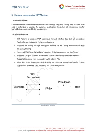
1 Hardware Accelerated HFT Platform
1.1 Business Context
Customer intended to develop a Hardware Accelerated High Frequency Trading (HFT) platform to be
used at exchange’s co-location. The customer specification stressed on sub-microsecond tick for
Market Data processing and Order Management.
1.2 Solution Overview
HFT Platform is based on FPGA accelerated Network Interface Card that will be used on
Trading Servers that exist in Exchange co-locations
Supports low latency and high throughput interface for the Trading Applications for High
Frequency Trading
Supports FPGA IPs for Market Data Processing, Order Management and Risk Control
Supports 10 Gigabit Ethernet interfaces for Market Data interface and Order Interface
Supports High Speed Host interface through 8 x Gen-3 PCIe
Linux Host Driver that supports User Friendly and Ultra-Low latency interfaces for Trading
Applications for Market Data processing and Order Management
Figure 1 Block Diagram
Exchange
FPGA
Host
PCIe Gen3
x8
10GE
Connections
2. FPGA CASE STUDY
#34, II Floor, 1st Main, 1st Block, Koramangala, Bangalore – 560 034
20 Feb, 2016, Page 2 Phone: +91-99451 16443 • contact@unizentechnologies.com • www.unizentechnologies.com
1.3 Features
Sub-Microsecond Latency for Market Data Processing & Order Management
Configurable & Friendly interfaces for Trading Applications
Independent Market data path and Order data path
Scalable architecture that supports easy adaptation for multiple exchanges
VHDL based HDL design
1.4 Challenges Addressed
Nano-second level optimizations in FPGA IPs
Ultra-low interrupt latency
Support for Very High Speed & Very High Volume of Market Data
Robust implementation to support peak data rates
3rd
Party IP integration
3. FPGA CASE STUDY
#34, II Floor, 1st Main, 1st Block, Koramangala, Bangalore – 560 034
20 Feb, 2016, Page 3 Phone: +91-99451 16443 • contact@unizentechnologies.com • www.unizentechnologies.com
2 Print Controller for HP Monochrome and Color Cartridge for a Hand Held
Mobile Printer
2.1 Business Context
Customer wanted to design a Handle Held printer using HP mono and colour cartridge. The customer
wanted a prototype with image sensor that tracks the motion and a print engine to print the data.
2.2 Solution Overview
The print controller provides control and data interface to HP driver ASIC that controls the HP
cartridge (Monochrome and Colour cartridges)
The FPGA controller interfaces optical sensor (SPI interface) and colour cartridges
The controller is aimed at sampling the sensor data to get real time position of the paper and
give it to OMAP through EMIF interface
The EMIF host controller is implemented in FPGA
The FPGA print controller is designed that drives the print data to colour cartridges in a
particular timing model as specified in the cartridge datasheet
Figure 2 Block Diagram
2.3 Features
Verilog Based HDL Design
Spartan 6 FPGA used to implement print controller
Pen warming algorithm development for cold start-up
The print controller engine consists of cartridge initialisation sequence and controlling timing
specific LVDS lines as specified by HP cartridge datasheet
Interrupt driven Print Data retrieved from OMAP through EMIF interface
2.4 Challenges Addressed
Developing HP Print Controller as per timing specification defined in the cartridge datasheet
Retrieving Print data from OMAP
Developing Pen warming algorithm in FPGA
Spartan 6 FPGA
TI OMAP
Processor
HP Cartridge
Driver ASIC
EMIF
MICCI Bus
LVDS
Lines
4. FPGA CASE STUDY
#34, II Floor, 1st Main, 1st Block, Koramangala, Bangalore – 560 034
20 Feb, 2016, Page 4 Phone: +91-99451 16443 • contact@unizentechnologies.com • www.unizentechnologies.com
3 Transmit Receive Multi Module (TRMM)
3.1 Business Context
Customer wanted a controller for Transmit Receive Multi Module. The scope of work included digital
control of Transmitter and Receiver modules along with a Flash memory controller. The customer
wanted to achieve Flash memory data transfer rate of 200 mega transfers per seconds.
3.2 Solution Overview
The FPGA controller implementation includes interface such as 1Gbit DDR2 SDRAM, SPI, I2C,
UART and RF Phase shifter and Attenuator digital control lines
NAND Flash controller for an 8GByte NAND Flash memory
NAND Flash is accessed one page at a time; erase to be done on a per-block basis, and written
sequentially
The design is targeted for Micron Technology SLC MT29F64G08ABCBB NAND flash device.
The controller is designed with NV-DDR2 interface aimed to obtain a data transfer rate of
200MT/s using ONFI 3.0 specification
The implementation has support for ECC using Hamming code algorithm
Figure 3 Block Diagram
Artix 7
FPGA
Host
Flash
Memory
TRMM
Modules
DDR2
5. FPGA CASE STUDY
#34, II Floor, 1st Main, 1st Block, Koramangala, Bangalore – 560 034
20 Feb, 2016, Page 5 Phone: +91-99451 16443 • contact@unizentechnologies.com • www.unizentechnologies.com
3.3 Features
Digital IO controls to control Transmit module
SPI interface to control the receive module
UART interface for Host communication
1Gbit DDR2 SDRAM access through Xilinx’s memory Interface Generator
8 Gbyte NAND Flash controller
VHDL Based HDL Design
3.4 Challenges Addressed
Development of 8 Gbyte NAND Flash Controller
MIG (Memory Interface Generator) IP core integration
6. FPGA CASE STUDY
#34, II Floor, 1st Main, 1st Block, Koramangala, Bangalore – 560 034
20 Feb, 2016, Page 6 Phone: +91-99451 16443 • contact@unizentechnologies.com • www.unizentechnologies.com
4 Debug Interface for a Custom Processor Architecture
4.1 Business Context
Customer wanted to integrate debugging interface for their custom processor. The customer required
complete hardware and software support for the debug interface.
4.2 Solution Overview
Unizen FPGA solution consists of the following
• Implementing JTAG TAP, Memory Access Port and Debug Controllers for supporting debug
interface for custom processor architecture as per ARM Debug Interface V5 specification
• Porting OpenOCD debug stack and GDB on a Linux Host, for the target processor architecture
• The List of Debug Controllers includes Processor Controller Block, Memory Bridge, Data Watch
Point & Trace Unit and ROM Tables
Figure 4 Block Diagram
7. FPGA CASE STUDY
#34, II Floor, 1st Main, 1st Block, Koramangala, Bangalore – 560 034
20 Feb, 2016, Page 7 Phone: +91-99451 16443 • contact@unizentechnologies.com • www.unizentechnologies.com
4.3 Features
• Halting the processor
• Hardware and Software Breakpoints
• Step execution
• Register access
• Access to all memory through DAP
• Processor reset and debugging reset event
• Halting and debugging the exceptions
• Hardware validation on Cyclone V FPGA
• Host interface through JTAG
• Verilog Based HDL Design
4.4 Challenges Addressed
Interface to remote GDB debug environment through OpenOCD
Developing RTL code for TAP & Debug Interface Port