More Related Content
Similar to Oliver toomey (20)
More from Dania Abdel-aziz
More from Dania Abdel-aziz (20)
Oliver toomey
- 1. 38 INGENIA INGENIA ISSUE 42 MARCH 2010 39
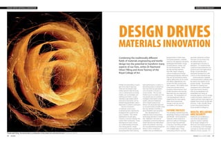
EMERGING TECHNOLOGYDESIGN DRIVES MATERIALS INNOVATION
DESIGN DRIVES
MATERIALS INNOVATION
Combining the traditionally different
fields of materials engineering and textile
design has the potential to transform many
aspects of our lives, writes Dr Raymond
Oliver FREng and Anne Toomey of the
Royal College of Art.
Textiles are everywhere, in every
part of our day-to-day lives.
There are micrometre-sized
textiles placed inside the body,
such as arterial stents;‘on-body’
textiles such as bandages and
clothing; and metre- or even
kilometre-scale textiles within
the built environment, such as
terraforming geotextiles used in
flood areas to prevent soil erosion.
Recent innovations
in materials science and
engineering have significantly
broadened the scope for the
uses of textiles. New textile
applications include glass,
ceramics, concrete, aramids and
carbon fibre composites. These
developments have moved
our understanding of textiles,
from being passive, simply
serving their design purposes of
being beautiful, hard wearing,
high performance or warm, to
becoming active or interactive.
One idea that has generated
a lot of interest is known as
‘smart’textiles. This has had
limited success to date, as it has
not proved easy to combine
intelligent information within
textiles, because traditional
silicon based systems and
devices are physically rigid and
so not particularly versatile, while
the very identity of textiles is
about flexibility and versatility.
New developments in
materials science and process
technology promise to change
this. Materials in the form of
conjugated conductive polymers,
where electrons are delocalised
within the polymer’s structure,
are now approaching amorphous
silicon in terms of electron
mobility and can therefore be
programmed in similar ways.
Functional polymeric materials
based on this approach are being
developed that exhibit a range
of useful electro-, photo- and
bio-active properties. There
are also existing materials
that offer shape-changing,
colour-changing and energy-
exchanging properties. Moreover,
they are not restricted to being
rigid or planar and can be woven
into fabrics, deposited as non-
woven thin films or processed
from solution. This enables them
to become printed sensors,
actuators, interconnectors and
simple transistors and even be
fabricated into very large (km2)
structures. The implications of
such developments offer an
opportunity for more radical,
rather than incremental,
change in the way we will
use textiles in the future.
FUTURE TEXTILES
The resulting materials have the
advantage of being conformable
and flexible. Active polymeric
materials which respond to
electrical, optical or biological
stimulus have the potential
to be spun into fibres, printed
as a coating or extruded as
thin multiple layers. These
three physical forms can then
generate interactive surfaces
and even 3D structures that
are determined by end-
use application, function or
aesthetics. To combine these
multifunctional properties into
products and new applications,
design should take place
alongside development, with
a focus on the individual user.
Active polymeric materials
can be processed in solution and
be used in the creation of 3D
product design. This provides
the basis for creating near-
transparent and conformable
logic and memory devices
that can be designed to be
embedded into nearly all
everyday objects, such as storage
surfaces, furniture, curtains and
carpets, and into many aspects of
people’s lives at work, at play and
at home. It also, critically, serves
to form the physical basis for
future Ambient Intelligence.
HEALTH, WELLBEING
AND SECURITY
Healthcare and wellbeing is
one of the key application
areas for smarter materials.
At the Royal College of Art
(RCA) we, and several partners,
are developing ‘smart’bandage
concepts to monitor and treat
different chronic wounds. If it
Textile Light Fitting. This reactive fabric is a combination of silver plated wire and luminescent yarn © Neil Musson MA RCA
- 2. 40 INGENIA INGENIA ISSUE 42 MARCH 2010 41
is possible to radically change
both the materials and the
construction processes of a
conventional bandage, there is
an opportunity, through design,
to change the perception and
experience of chronic wounds
from both the patient’s and the
carer’s viewpoint.
With smart bandages, the
advantage of incorporating
wireless technology along
with therapeutic delivery, for
example, would mean that
medical staff wouldn’t need to
remove the bandage to monitor
the wound. Continuous and long
term monitoring will make the
bandages more cost-effective by
saving staff time. In addition, skin
conductivity sensors can monitor
patient stress and anxiety in order
to continually assess patient’s
comfort and wellbeing.
Our proposal, which includes
eight university, research institute
and industry groups, will look at
ways to control pressure and fluid
monitoring. The RCA team will
work on the design of the new
bandage, including the fabrics
and the‘soft engineering’of the
bandage itself.
A related example being
developed is eScent, a wearable
technology that releases different
scents depending on the time
of day and therefore whether
it is being worn to a business
meeting or at a nightclub.
This concept is based on MEMS
(micro-electro-mechanical
systems) technology combined
with a bio-responsive material
containing a fragrance. The
material can expand in response
to an electrical impulse, triggered
by, for example, sensing a pH
change or sound, and release
the fragrance. The beauty of this
is that the process is reversible;
when the triggering signal is
removed, the material returns to
its original state. This work is a
collaboration between the Royal
College of Art and Central Saint
Martins (Dr J Tillotson) and an
industrial partner. The controlled
release and targeted delivery
methodology also has significant
potential for healthcare too.
Security is another area
where smarter textiles can
play a role. We are looking at
the potential to incorporate
holographic materials or
quantum dots into bank notes.
These tiny materials are invisible
to the human eye (quantum
dots are of the order of a
nanometre in diameter) but
have characteristic responses
Sensor Smart delivery
Product design envelope and wearable assemblages
Signal
acquisition,
storage,
computation,
transmission
O2
Bioactive
molecules
O2
pH
ROS
enzymes
wirelesswireless
ACTIVE BANDAGE
containing bio-compatible
polymers
WOUND
smart trigger
Figure 1: Conceptual‘smart’ bandage construction
with other smart material
properties in textiles in the built
environment, such as curtains,
wallpaper, furniture and carpets.
Organic photovoltaics are
another interesting area utilising
large area, thin electro/photo
active films for development
(see Plastic Solar Cell
Development). One of the most
promising approaches to date
is based on combining the
nanostructured active polymer
poly (3-hexyl thiophene) (P3HT)
and the fullerene derivative
6,6-phenyl C61 butyric acid
methyl ester (PCBM). However,
in order for such systems to be
truly revolutionary, they will
not only need long lifetimes
and better photo-conversion
efficiency (their efficiencies
are still significantly lower
than that of their inorganic
counterparts), they will also
have to be fabricated by the
square kilometre. This will
mean reel-to-reel printing
technology equivalent to today’s
modern newspaper presses,
using either gravure or offset
printing or even multilayer thin
film extrusion. Such technology
paves the way for incorporating
solar energy harvesting and
energy storage and printing it by
the square metre into wallpaper,
for example.
A COMBINED
APPROACH
Such exciting possibilities
require a new way of thinking.
The phenomenal success of
the iPod (which is based on
traditional silicon technology)
has highlighted the importance
of strong, user-focused
design. Similarly, to make the
most of the opportunities of
smart materials, engineers
and designers need to work
together from the start.
Having engineers involved
in the design process
dramatically increases the
designer’s knowledge of the
performance potential of
materials that could be used
and their properties. It also
shortens the development
time for new materials and
production implementation.
It means that designers can
think about innovative future
products before the materials
to achieve them become
available. On the other hand,
it also means that designers,
who are focused on the
possibilities for end-users, can
contribute in the early stages
of developing materials with
particular properties.
The interdisciplinary
nature of design, materials
and engineering finds
common ground through
the opportunities offered by
programmable, interactive
surfaces and structures. The
breadth and depth of human-
centred applications presented
by these structures form the
basis of ‘materials for living’.
The Royal College of Art has
a team that includes chemical
and material engineers working
directly with designers. They
are together looking at the
commercial potential of new
materials based on conjugated
polymers with conformable
properties which are solution
processable. The engineers
are used to dealing with
systems and materials while the
designers deal with materials
and societal needs.
Materials are the
common thread that runs
through both approaches
and forms the basis for our
discussions. Because many
of the potential materials we
are looking at are solution-
processable, we can consider
materials as dots (derived
from droplet and spray
production followed by phase
transformation), lines (from fibre
spinning and subsequent phase
transformation), surfaces (from
thin film, multilayer extrusion and
deposition) and structures (from
rapid prototyping, 3D printing
and injection moulding).
Looking through a concrete wall. Light-transmitting concrete blocks can
be embedded with luminous optical glass fibres. At up to 500mm thick,
the blocks can be used to build a wall several metres in thickness. Light
information from one side of the concrete, such as a shadow, is replicated by
optical fibres embedded in the opposite side © Litracon
to light. Incorporated into
currency, or anything else,
they can act like a tiny barcode
giving a distinct pattern of
multiple colours.
SMARTER BUILT
ENVIRONMENTS
The built environment is
an important opportunity
for ‘smarter’materials too.
Compared to automotive or
aerospace construction, most
building interiors are inactive.
Buildings consist of many
surfaces and interfaces and,
today, functionality, such as
lighting and communication,
is added on with various
manually activated surface
switches. By incorporating
new smart materials into the
surfaces and interfaces of
buildings the actual functionality
can be embedded into surfaces
that are able to perform more
than one action.
There are already some
interesting developments in the
area of architectural lighting.
Multiple electro- and photo-
active polymer-thin films are
layered on top of one another
to yield solid state lighting
surfaces, as well as the colour or
gradient of light. This signals the
beginning of the architectural
use of organic light emitting
diodes (OLEDs) from surfaces
that emit light, rather than
the traditional sources of light
offered by incandescent bulbs.
There are interesting possibilities,
too, for incorporating fluorescent
and phosphorescent fibres
Silicon wafers
Poly Silicon
Hydrogenated amorphous
Silicon (a-Si:H)
Polythiophene
Pentacene
Advanced
Organic
CMOS
1984 1988 1992 1996 2000 2004 2008 2012
10-6
10-5
10-4
10-3
10-2
10-1
1
10
102
103
Mobility(cm2/Vsec)
Low-cost embedded intelligence (AmI), i-packaging, smart cards,
i-textiles, organic PV, SS light, e-light, signage, advertising
SEMICONDUCTOR PERFORMANCE EVOLUTION
Figure 2: Graph showing the space for product applications using advanced
organic Complimentary Metal-Oxide Semiconductors (CMOS)
EMERGING TECHNOLOGYDESIGN DRIVES MATERIALS INNOVATION
- 3. 42 INGENIA INGENIA ISSUE 42 MARCH 2010 43
BIOGRAPHIES – Dr Raymond Oliver and Anne Toomey
Dr Raymond Oliver FREng is Director, Arrow Science
Consulting. Previously, as an ICI Fellow, he led applied research
into advanced materials and novel processes and later became
Director, Science and Innovation at the Centre for Nano,
Micro and Photonic Systems. At the Royal College of Art, he is
engaged in the development of a physical basis for Ambient
Living through intelligent materials and interactive surfaces.
Anne Toomey joined the Royal College of Art in 1998 and
is currently the Deputy Head of the Textiles Department.
She is a printed textiles specialist with UK and international
experience in design, product development, manufacture
and education. Research is focused on design-led innovation
with advanced materials, in particular intelligent and
responsive surfaces, to redefine the relationship between
product and the human experience.
The authors would like to thank Dr Siân Harris for her help in the writing
of this article.
DESIGN TO PRODUCT
There is strong interest in
our approach to design with
smarter materials from a range
of industrial groups. These
include the aerospace industry,
architects, engineering suppliers
in the construction industry
interested in using interactive
surfaces, the pharma delivery
systems industry and developers
of wearable technology. The key
challenge is turning the designs
into real products and systems, a
result of the restricted availability
of active materials in design
friendly formats.
We are currently discussing
with material laboratories and
companies about the sourcing
of materials to incorporate into
our designs. A current challenge
is obtaining sufficient quantities
of materials. Many academic
materials laboratories produce
suitable quantities to be able to
test the properties and publish
the results in research papers –
but not enough to be able to
incorporate into implementable
design led products.
MANUFACTURING
CHALLENGES
There are also manufacturing
challenges to be addressed.
First, there is the problem of
how to create active electro-,
photo- and bio- materials that
are highly reproducible and
reliable and can be processed in
A good example of large-area non-woven thin films is the
development of organic and organic/inorganic photovoltaic
devices driven by the global need for low-cost (comparable
to current fossil fuels), portable (off-grid) power which can be
conveniently applied in regions of harsh or extreme climatic
environments or be easily located close to sources of seawater
(ease of de-salination).
The use of printable, thin-film, non-woven plastic solar cells
constructs to harvest solar radiation (photons) and be converted
to power (photo-electric current) is driven by cost and device
development considerations. The conversion efficiency (photon
to electron) of these materials has risen rapidly in the last five years
from less than 1% to more than 8% and will reach an economically
favourable value of 10% by 2012.
To create one gigawatt of power will require approximately
10km2 of ‘solar wallpaper’, which is made up of 70 nanometre
thin films to ensure no ‘electron-hole’recombination that would
diminish the solar cell efficiency. The engineering challenge is to
create large areas of actively coated polymer film multilayers that
are, in total, less than one micron thick. Fortunately, ‘reel to reel’
polymer extrusion lines have demonstrated the ability to generate
some 10km2/month in the production of thin film polyethylene
terephthalate (PET). If the deposition and molecular transportation
processes work effectively, then gigawatt power production will be
realistic within five years at a cost that is comparable to that of fossil
fuels (less than 22 pence per watt at peak times).
When combined with equivalent printed storage (thin film
batteries or supercapacitors) and printable light organic light
emitting diodes or solid state lighting, there is great potential
to create portable off-grid power that will have significant
benefits for heating, lighting and even healthcare (low-cost
clean water or fridge operation, for example) in regions of
extreme climate.
PLASTIC SOLAR CELL DEVELOPMENT
All-printed transparent plastic solar cell using web based printing
technology. These are completely transparent and printed directly,
without a vacuum process © VTT Technical Research Centre for Finland, Oulu
a way that allows the formation
of fibres, fabrics and ultra-thin
films capable of being produced
with large surface areas. Here,
electrospinning and thin-film
multilayer extrusion provide us
with implementable technology
solutions which are also capable
of scale up.
A second challenge is that
the effectiveness of most of the
organic conductive polymers of
interest is rapidly diminished in
the presence of oxygen and/or
moisture. This means that,
in parallel with their production,
comes the need to create
protective, encapsulating
films that allow long operating
lifetimes. An alternative
approach of course is to
Electroluminescent lighting constructed onto a leather substrate based on PEDOT:PSS and zinc sulphide doped phosphor ink. Future uses include room interior
decoration and furniture surface covers © Ana Pineyro/Project funded by CETEMMSA Technology Centre and FAD (Foment de les Arts i del Disseny)
build into the conjugated
conductive polymers stabilising
molecules that act or react
internally to achieve the
equivalent of a relatively
expensive external organic-
inorganic encapsulating
protective coating.
The third challenge is that
the idea of creating organic
Complementary Metal-Oxide
Semiconductor (CMOS)
technology relies both on
the solution processability of
the active materials and on
the ability to generate higher
mobilities. The most promising
manufacturing approaches for
these materials today are: rapid
prototyping, where successive
layers of the required materials
are built up according to the
manufacturing design from a
computer-aided design package;
layer-by-layer deposition; and
atomic layer deposition.
AMBIENT
INTELLIGENCE
Smarter materials also bring
other, societal, challenges that
need to be addressed. Once
people begin to interact and
share information more with
textiles and material surfaces
and interfaces within, on and
near their bodies, questions
of control, trust and privacy
emerge, as well as fears
about information overload.
These aspects could delay
the introduction of novel
technologies into our everyday
lives. This area of social as well
as system intelligence is a key
to successful and ubiquitous
uptake. In healthcare in
particular, there is a clear need
for standards in this area.
Economies of scale will reduce
the cost of incorporating
‘intelligent’textile surfaces into
products and from here we will
move into a new era of smart
environment development,
which generates the physical
basis for future Ambient
Intelligence (AmI).
Smarter textiles and
intelligent materials are an
emerging technology. The
materials which drive this, that
is electro-, photo-, and bio-active
polymers and gels, have only
been in development within
the last 10 to 15 years.
However, all the indications
suggest that AmI is going to
be a key strategic driver for
future applications in printed
electronics and photonics, which
is design-led, needs-driven but
materials-anchored.
Further information
www.arrowscience.com
www.rca.ac.uk
Ambient Intelligence is going to be a key
strategic driver for future applications in
printed electronics and photonics.
EMERGING TECHNOLOGYDESIGN DRIVES MATERIALS INNOVATION