Download to read offline
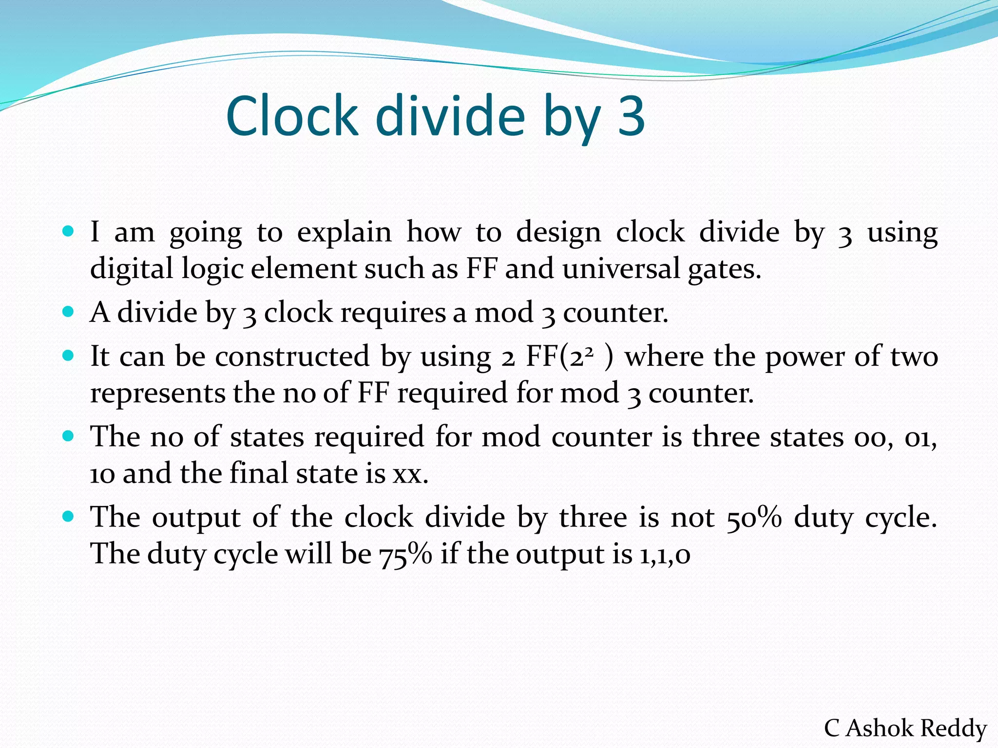
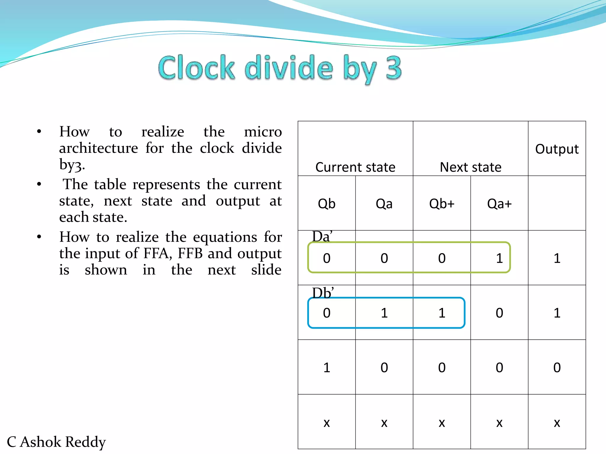
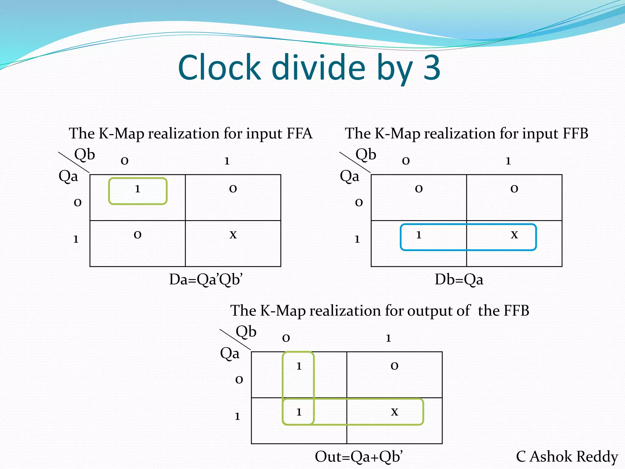
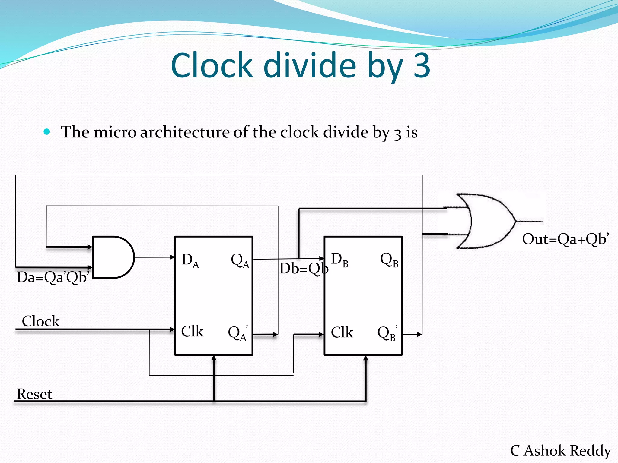
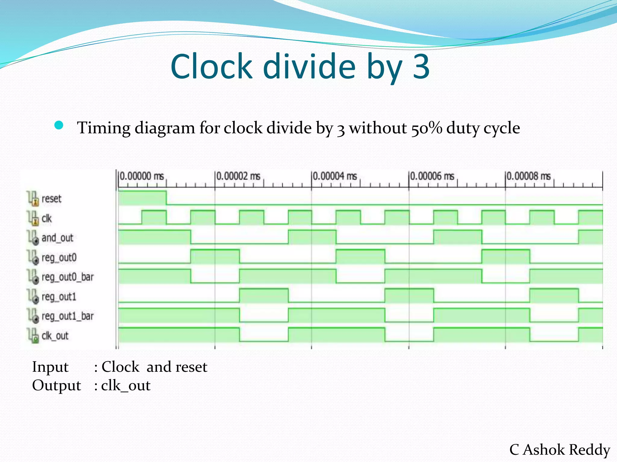
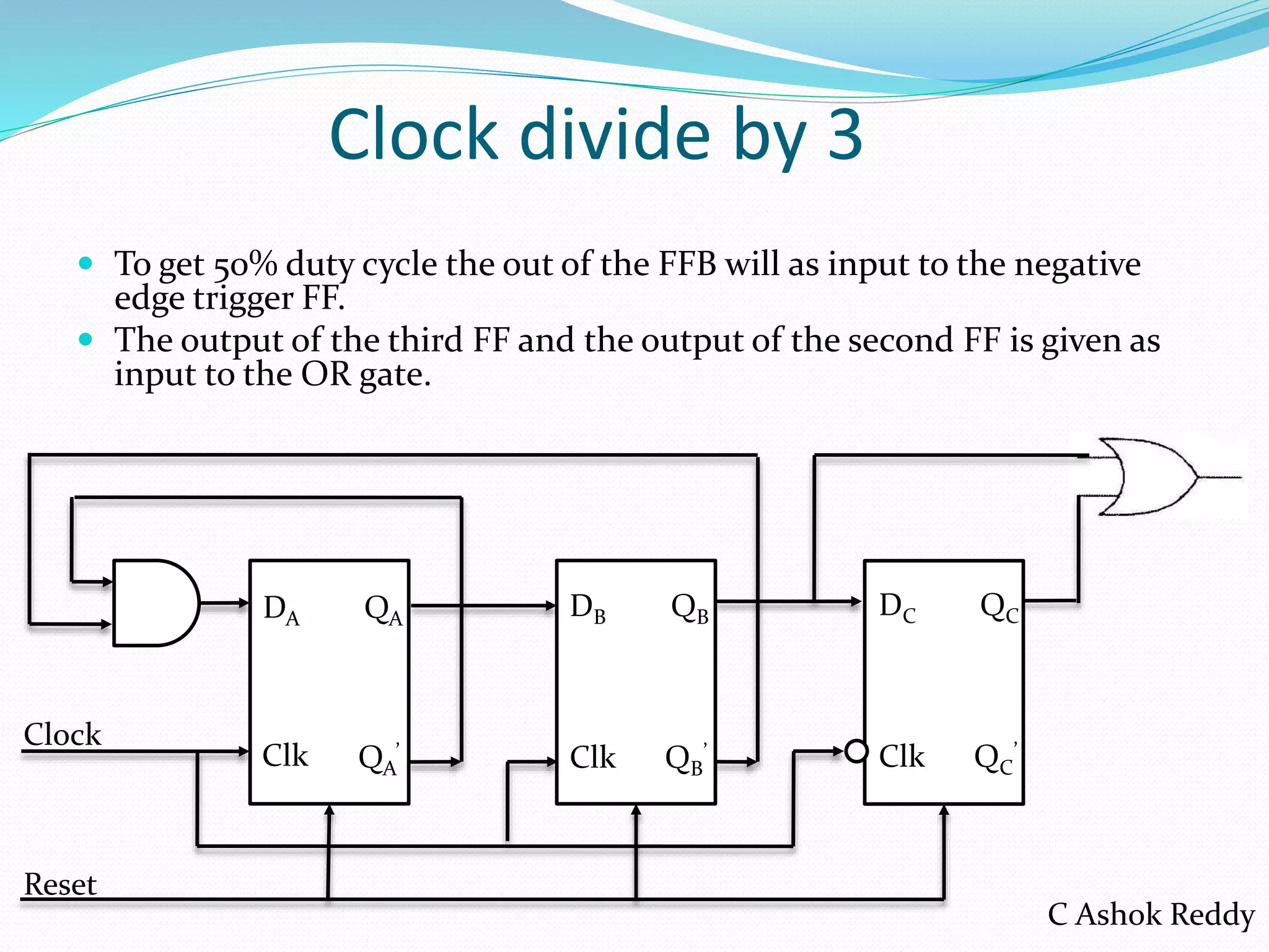
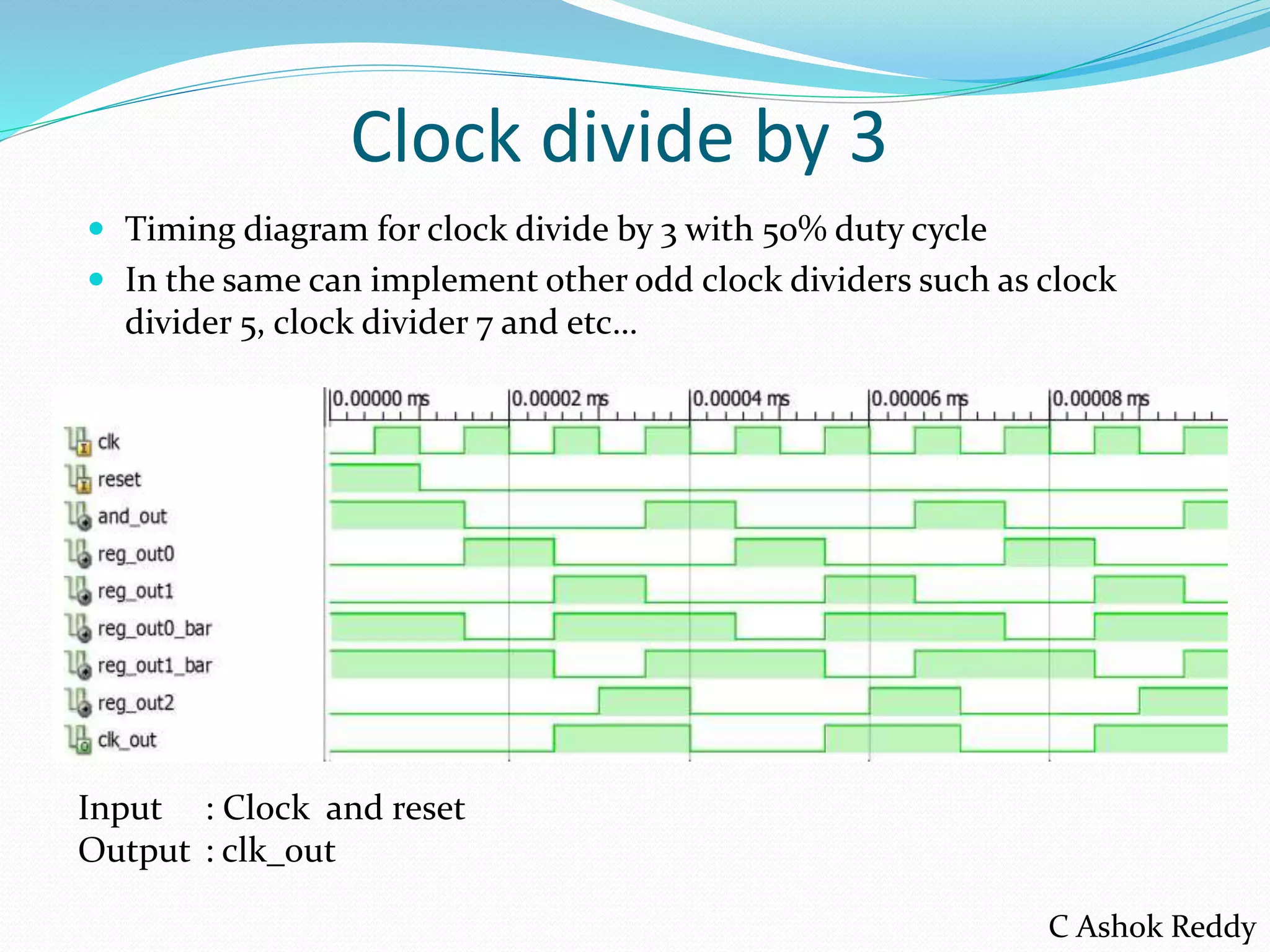


The document describes how to design a clock divider by 3 using digital logic elements like flip-flops and gates. A mod 3 counter using two flip-flops is used, with states 00, 01, 10. The output is not 50% duty cycle initially but can be made 50% by adding a third flip-flop. Diagrams show the logic implementation and timing diagrams for both with and without 50% duty cycle output.