
Recommended
Recommended
More Related Content
What's hot
What's hot (19)
Viewers also liked
Viewers also liked (10)
Similar to July 24, 2003
Similar to July 24, 2003 (20)
Recently uploaded
Recently uploaded (20)
July 24, 2003
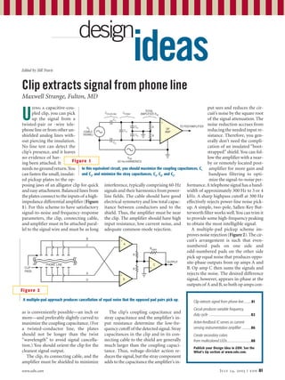
- 1. www.edn.com July 24, 2003 | edn 81 ideas design Edited by Bill Travis U sing a capacitive-cou- pled clip, you can pick up the signal from a twisted-pair or -wire tele- phone line or from other un- shielded analog lines with- out piercing the insulation. No line test can detect the clip’s presence, and it leaves no evidence of hav- ing been attached. It needs no ground return.You can fasten the small, insulat- ed pickup plates to the op- posing jaws of an alligator clip for quick and easy attachment.Balanced lines from the plates connect to the inputs of a high- impedance differential amplifier (Figure 1). For this scheme to have satisfactory signal-to-noise and frequency-response parameters, the clip, connecting cable, and amplifier must m be attached paral- lel to the signal wire and must be as long as is conveniently possible—an inch or more—and preferably slightly curved to maximize the coupling capacitance. (For a twisted-conductor line, the plates should not be longer than the twist “wavelength” to avoid signal cancella- tion.) You should orient the clip for the cleanest signal output. The clip, its connecting cable, and the amplifier must be shielded to minimize interference, typically comprising 60-Hz signals and their harmonics from power- line fields. The cable should have good electrical symmetry and low total capac- itance between conductors and to the shield. Thus, the amplifier must be near the clip. The amplifier should have high input resistance, low current noise, and adequate common-mode rejection. The clip’s coupling capacitance and stray capacitance and the amplifier’s in- put resistance determine the low-fre- quency cutoff of the detected signal.Stray capacitances in the clip and in its con- necting cable to the shield are generally much larger than the coupling capaci- tance. Thus, voltage-divider action re- duces the signal,but the stray component adds to the capacitance the amplifier’s in- put sees and reduces the cir- cuit’s noise by the square root of the signal attenuation. The noise reduction accrues from reducing the needed input re- sistance. Therefore, you gen- erally don’t need the compli- cation of an insulated “boot- strapped” shield. You can fol- low the amplifier with a near- by or remotely located post- amplifier for more gain and bandpass filtering to opti- mize the signal-to-noise per- formance.A telephone signal has a band- width of approximately 300 Hz to 3 or 4 kHz. A sharp highpass cutoff at 300 Hz effectively rejects power-line noise pick- up. A simple, two-pole, Sallen-Key But- terworth filter works well.You can trim it to provide some high-frequency peaking to obtain the most intelligible signal. A multiple-pad pickup scheme im- proves noise rejection (Figure2).The cir- cuit’s arrangement is such that even- numbered pads on one side and odd-numbered pads on the other side pick up equal noise that produces oppo- site-phase outputs from op amps A and B. Op amp C then sums the signals and rejects the noise. The desired difference signal, however, appears in-phase at the outputs of A and B,so both op amps con- + – TO POSTAMPLIFIER OP AMP R RVS (CABLE SIGNAL) VCM 60 Hz+HARMONICS C1 CCOUPLING CSTRAY TOTAL AMPLIFIER RIN C2 C3 C4 C5 Figure 1 Clip extracts signal from phone line Maxwell Strange, Fulton, MD In this equivalent circuit, you should maximize the coupling capacitances, C1 and C2 , and minimize the stray capacitances, C3 , C4 , and C5 . + – C + – B + – A RGAIN OUTPUT R R A D B C PHONE LINE CLIP PADS Figure 2 A multiple-pad approach produces cancellation of equal noise that the opposed pad pairs pick up. Clip extracts signal from phone line..........81 Circuit produces variable frequency, duty cycle ........................................................82 Active-feedback IC serves as current- sensing instrumentation amplifier ............86 Create secondary colors from multicolored LEDs................................88 Publish your Design Idea in EDN. See the What’s Up section at www.edn.com.
- 2. 82 edn | July 24, 2003 www.edn.com ideas design tribute equally to the output. You can make a segmented pickup from pieces of two-sided pc board with the solid-copper side serving as a shield.You can solder the shield side of the pieces to a suitable alli- gator clip. Alternatively, for longer term use, you can simply tape them onto the cable. You can use any even number of pads. the more you use, the better, but eight on each side are sufficient. The amplifier of Figure 3 uses two quad J-FET or BiFET op amps.Thanks to stray capacitance on the input lines of the test model, a relatively low input resist- ance of 3.3 M⍀ is sufficient. Input noise is mostly the Johnson noise of the 10-M⍀ feedback resistors.Power-line noise pick- up is usually the bigger problem. The output stages incorporate some highpass filtering to reject noise below 300 Hz.The output level depends on many factors but is approximately 50 mV. A postamplifier (not shown) can provide more equaliza- tion, filtering, and gain if necessary, as well as manual or automatic level control. Tests of models of both design ap- proaches use readily available compo- nents and show perfectly clear telephone speech through a small speaker in the postamplifier box. The multiple-pad pickup system produces noticeably low- er noise, and clip orientation is less crit- ical.˿ _ + IC1B _ + IC1A _ + IC2A _ + IC2C NOTES: IC1 AND IC2 ARE QUAD JFET OP AMPS. CAPACITORS ARE Ϯ20% CERAMIC._ + IC1D _ + IC1C _ + IC2B 3.3M D C B A 3.3M 10M 10M 10M 10MINPUT FROM MULTISEGMENT PICKUP 3.3M X X 9V SHIELD AND POWER GROUND SHIELD 3.3M 3.3M 3.3M R 150k R R 150k 0.0015 µF 0.01 µF 0.01 µF 1 µF 1 µF 1 µF 150k 10k OP-AMP +POWER OP-AMP מPOWER 220k R R R 150k OUTPUT 3.3k 150 pF _ + IC2D R Figure 3 This amplifier, using the multiple-pad approach effectively reduces power-line-related noise pickup. T his Design Idea shows a simple, low-cost circuit that produces a high- ly accurate variable-frequency and variable-duty-cycle output (Figure 1). Further, the duty cycle and frequency are independent of each other (excluding 0 and 100% duty cycle). The method de- rives its accuracy and stability from the fact that the output is based on a crystal oscillator and divisions of the oscillator’s frequency. The design uses only six de- vices. IC1 , a 74HC393 binary ripple counter, has as its input is the oscillator’s output frequency.The outputs are the os- cillator frequency divided by two, four, eight, 16, 32, 64, 128, and 256. IC5B is cas- caded with IC1 to divide the oscillator fre- quency further by 512, 1024, 2048, and 4096. In this circuit, the divide-by-128 is the largest division it uses. You could, with a simple wiring change, substitute an unused divider to obtain a different output-frequency range.The eight inputs of IC2 ,a 74HC151 eight-line-to-one-line multiplexer, connect to the oscillator’s frequency divided by one, two, four, eight, 16, 32, 64, and 128. Note that the oscillator’s output connects directly to an input of IC2 . This connection allows se- lecting the oscillator’s frequency divided by one. IC2 connects one of the eight fre- quencies to the input of IC3 . IC3 , a 74HC4017 decade counter, di- Circuit produces variable frequency, duty cycle Mark Reed, Texas Instruments, Dallas, TX
- 3. 84 edn | July 24, 2003 www.edn.com ideas design vides the frequency from IC2 ’s output by 10. Therefore, the maximum output fre- quency for this design is the oscillator fre- quency divided by 10. Each of the decod- ed decade counter’s 10 outputs goes high for one clock cycle only (Figure 2). Using the 10 outputs, a fre- quency’s period divides into 10 equal intervals.You can use these 10 equal intervals to generate duty cycles of 10, 20, 30, 40, 50, 60, 70, 80, and 90%. For this circuit, the outputs of IC3 , Q1 through Q8, yield the end-of-pulse signals for duty cy- cles of 10 through 80%, respec- tively.The start-of-pulse signal is Q9’s negative edge,which occurs at the same time as Q0’s positive edge. Therefore, you can use Q9 as start-of-pulse low true, and the end-of-pulse signals are high true. The eight inputs of IC4 , an eight-line-to-one-line multi- plexer, connect to eight of the nine end-of-pulse outputs from IC3 . This circuit omits the 90% duty cycle. You can include the 90% duty cycle with a simple wiring change. If you want to select 0% duty cycle,connect an input to IC4 .If you select 0% duty cycle, the generator’s out- put is low. IC4 connects one of eight end- of-pulse signals to IC5 . IC5A is a binary ripple counter that serves as a set-reset latch. The start-of- pulse signal sets the latch. The end-of- pulse signal resets the latch. The output of IC5 is the variable-frequency and vari- able-duty-cycle output of the signal generator. For example, if the oscillator’s frequency is 4 MHz and IC2 ’s C B A inputs are 0 1 0, then the generator delivers 100 kHz.If IC4 ’s C BA inputs are 0 0 1, then the gen- erator’s output exhibits 20% duty cycle.If you need to select from more than eight fre- quencies, use a larger multi- plexer than IC2 . Cascade more or different types of dividers to achieve your frequency needs. You can use a 74HC390 to ob- tain division by five, 10, 50, 100, and so on. If you need other duty cycles, cascade 74HC4017s to divide the pe- riod by the desired number of intervals. Finally, if you need to select from more than eight duty cycles, use a larger mul- tiplexer than IC4 .˿ CLK Q0 Q1 Q2 Q3 Q4 Q5 Q6 Q7 Q8 Q9 START-OF-PULSE END-OF-PULSE 10% DUTY CYCLE END-OF-PULSE 20% DUTY CYCLE END-OF-PULSE 30% DUTY CYCLE END-OF-PULSE 40% DUTY CYCLE END-OF-PULSE 50% DUTY CYCLE END-OF-PULSE 60% DUTY CYCLE END-OF-PULSE 70% DUTY CYCLE END-OF-PULSE 80% DUTY CYCLE END-OF-PULSE 90% DUTY CYCLE IC3 Figure 2 The end-of-pulse signals from IC4 determine the duty cycle of the output waveform. QA QB QC QDCLR 11 /512 /1024 /2048 /4096 10 9 812 13 IC5A QA QB QC QDCLR 11 10 9 812 DGND 7 DGND DGND 13 IC1B QA 5V Y1 QB QC QDCLR Q0 Q1 Q2 Q3 Q4 Q5 Q6 Q7 Q8 Q9 CO CLK 3 4 5 62 DGNDDGND GND OUT EN 1 1 4 5 8 CLK CLK IC1AVCC IC3 12 13 14 15 6 5 14 13 15 1 2 3 SET FREQUENCY 4 9 10 11 /128 /256 /64 /32 /16 /8 /4 /2 /1 CI CLK RST 7 DGND C B A OSCILLATOR FREQUENCY DIVIDE BY 0 0 0 0 1 1 1 1 0 0 1 1 0 0 1 1 0 1 0 1 0 1 0 1 10 20 40 80 160 320 640 1280 DGND A B C D0 D1 D2 D3 D4 D5 D6 D7 IC4 IC5B 12 13 14 15 6 5 1 2 START OF PULSE END OF PULSE 1 2 3 SET DUTY CYCLE 4 9 10 11 80% 70% 60% 50% 40% 30% 20% 10% W Y 12 3 11 9 6 5 1 10 7 4 2 QA QB QC QD 3 1 GENERATOR OUTPUT 4 5 6 C B A DUTY CYCLE (%) 0 0 0 0 1 1 1 1 0 0 1 1 0 0 1 1 0 1 0 1 0 1 0 1 10 20 30 40 50 60 70 80 74HC393N 74HC393N 74HC393N G A B C D0 D1 D2 D3 D4 D5 D6 D7 IC2 W Y 74HC151N 74HC151N 74HC393N 74HC4017N SET_FREQ_C SET_FREQ_B SET_FREQ_A SET_DUTY_C SET_DUTY_B SET_DUTY_A CLR CLK G Figure 1 This circuit produces waveforms of variable frequency and duty cycle. Further, the frequency and duty cycle are independent of each other.
- 4. 86 edn | July 24, 2003 www.edn.com ideas design H igh-speed current sensing presents a de- signer with some sig- nificant challenges. Most techniques for sensing cur- rent involve measuring the differential voltage the cur- rent produces as it flows through a sense element, such as a resistor or a Hall-effect device. The differential voltage across the sense element is gener- ally small and is often riding on a common-mode voltage that is considerably larger than the differential voltage itself. Accurate amplifica- tion of the differential voltage requires a differential amplifier with high input im- pedance, high CMR (common-mode re- jection); wide input-common-mode voltage range; and high, well-defined gain.Traditional instrumentation ampli- fiers have these features and often serve for low-frequency current sensing, but they perform poorly at high speeds. High-speed current sensing requires the kind of performance that instrumenta- tion amps provide, but their abilities must extend to high fre- quencies. Figure 1 shows how high-speed active feedback amplifiers, such as the AD8129 and AD- 8130 differential receivers, are ideal for these high- speed instrumentation- amp applications. The AD8129 requires a mini- mum closed-loop voltage gain of 10 for stability, whereas the AD8130 is unity-gain-stable. Active-feedback ampli- fier operation differs from that of traditional op amps; it provides a beneficial separation between the sig- nal input and the feedback network. Figure 1 shows a high-level block dia- gram of an active-feedback amplifier in a typical closed-loop configuration. High-speed current sensing uses a re- sistor as the sense element. The input stages are high-impedance, high-CMR, wideband, high-gain transconductance amplifiers with closely matched trans- conductance parameters. The output currents of the transconductance am- plifiers undergo summing, and the voltage at the summing node is buffered to provide a low-impedance output. Applying negative feedback around amplifier B drives VOUT to a lev- el that forces the input voltage of am- plifier B to equal the negative value of the input voltage at amplifier A, be- cause the current from amplifier A equals the negative value of the current from amplifier B, and the gm values are closely matched. From the foregoing discussion, you can express the closed- loop voltage gain for the ideal case as: VOUT /VIN ϭ1ϩRF /RG ϵAV . Measurement sensitivity in volts per ampisexpressedas:VOUT /ISENSE ϭAV RSENSE . Minimizing the values of RF and RG also minimizes resistor and output-voltage noise arising from input-referred current + + – – + – gm A + – gm B ISENSE RSENSE RF RG IOUT VOUT VSENSE ϫ1 AD8129/30 Figure 1 Active-feedback IC serves as current-sensing instrumentation amplifier Jonathan Pearson, Analog Devices, Wilmington, MA An active-feedback amplifier is ideal for current-sensing applications. + – gm + –50 ϫ1 AD8129 1 33 pF 33 pF50 NETWORK-ANALYZER Rx NETWORK-ANALYZER Tx 150 nH 100-MHz, THREE-POLE BUTTERWORTH LOWPASS FILTER 50 50 15.8 301 gm Figure 2 This test circuit produces flat frequency response to 10 MHz.
- 5. 88 edn | July 24, 2003 www.edn.com ideas design noise. Because of the small sense resist- ance and high measurement frequencies, you must minimize parasitic effects in the input circuitry to avoid measurement er- rors. Parasitic trace inductance in series with the sense element is of particular concern,because it causes the impedance across the amplifier’s input to increase with increasing frequency, producing a spurious increase in output voltage at high frequencies. Figure 2 illustrates a test circuit with RSENSE ϭ1⍀ and AV ϭ20, which equates to a measurement sensi- tivity of 20V/A. The three-pole lowpass filter produces a defined bandwidth and attenuates spurious responses at the am- plifier’s output arising from input signals at frequencies outside the desired meas- urement bandwidth.The test circuit’s fre- quency response in Figure 3 shows that the expected differential-to-single-ended gain of 20/101, or Ϫ14 dB, is flat to approximately 10 MHz and is down by 3 dB at 62 MHz. Figure 3 demon- strates the effectiveness of the high CMR of active-feedback amplifiers. The com- mon-mode signal at the amplifier’s input is approximately 50 times greater than the differential signal across the sense re- sistor.˿ Figure 3 The test circuit in Figure 2 exhibits accurate differential gain in the presence of large com- mon-mode signals. I t is well-known that simultaneous- ly mixing two primary-color light sources,such as red and green,creates a secondary color, such as yellow. This mixing process commonly occurs in tri- color LEDs. One disadvantage of this method of generating a yellow color is that the LED must use twice the cur- rent because both the red and the green LEDs must be on. In battery-pow- ered circuits,the LED indicator’s operat- ing current may be a significant fraction of the supply current, so using the same current to generate both primary and secondary colors is advantageous. The operating-current savings may be signif- icant in telecom-line-card applications involving thousands of line cards or large-panel RGB LED displays. This De- sign Idea proposes a sequencing method to generate balanced secondary colors from bicolor,tricolor,and RGB LEDs,us- ing only one LED’s operating cur- rent.Advantages include lower pow- er dissipation and more uniform in- tensities between primary and secondary colors.Using the sequencing method also allows a bicolor LED to now produce three colors and keep a simpler pc-board layout using two rather than three pins. In addition, you can also produce white light with RGB LEDs using the sequenc- ing method. The method uses the property of im- ages to persist in the human eye for sev- eral tens of milliseconds. If different pri- mary colors flash sequentially and quick- ly enough from one point, humans see them as overlapping in time, and the brain interprets them to appear as sec- ondary colors or even white, depending on the color components. Experimenta- tion with two or three primary-color LEDs shows that the flash sequence must complete within approximately 25 msec or less to produce a solid secondary col- or or white light. In testing for an upper limit, you can use flash rates to 1 MHz to produce this effect without degrading secondary colors. Thus, you can use any convenient clock source higher than 40 Hz to create secondary colors. Note that R1 R4 VCC R2 A B RC GC CA LED 1 BILEDCA R5 VCC R7 A C RC BC R6 B GC CA LED 4 TRILEDCA VCC A B RC R3 B A RC GC GC CA LED 2 BILEDCA LED 3 BILED NOTES: CA=COMMON ANODE. CC=COMMON CATHODE. Figure 1 Create secondary colors from multicolored LEDs Claude Haridge, Stittsville, ON, Canada All these LED configurations can produce secondary colors, either by current control or duty-cycle control. LEDs OFF RED LED ON GREEN LED ON YELLOW f>40 Hz 5V 0V 5V 0V A B 5V 0V 5V 0V A B tGREEN tRED t<25 mSEC Figure 2 The waveforms at the top generate yellow from green and red; the same result ensues from duty-cycle control (bottom right).
- 6. 90 edn | July 24, 2003 www.edn.com ideas design the primary-color LEDs must be physi- cally close together, such as on a semi- conductor chip, for the eye to properly mix the light. Diffused lenses also allow a wider viewing angle. These combina- tions are commercially avail- able as bicolor, tricolor, and RGB LEDs. Figure 1 shows the various LED-circuit configurations, and Figure 2 shows the timing to generate all three colors from bicolor and tricolor LEDs, although using only one LED’s operating current. Note that the driver for the bicolor LED must be able to sink and source cur- rent.You may have to provide color bal- ance between the primary-color LEDs to ensure that the secondary colors appear properly. The LEDs have different effi- ciencies and intensities as the human eye sees them, and these parameters need correcting. For tricolor LEDs in a com- mon-anode or -cathode configuration and 50% duty cycle, the correction is easy to effect by adjusting the current- limiting resistors. Alternatively, you can use one current-limiting resistor and then vary the duty cycle to provide the necessary color balance.For two-leaded, bicolor LEDs, it is easier to adjust the duty cycle to produce the correct sec- ondary color than to use additional cir- cuitry. The waveforms at the bottom of Figure 2 illustrate duty-cycle control to achieve secondary-color balance for both bicolor and tricolor LEDs. Using a sequenced bicolor LED to generate three colors has packaging ad- vantages, particularly when you verti- cally stack several LEDs. Previously, stacked, tricolor LEDs need- ed to use a through-hole as- sembly, because the middle lead would be inaccessible if the devices were surface- mounted. Because the bi- color LED has only two pins, you can vertically stack several of them and bend out the leads for surface mounting. The generation of secondary colors can also extend to RGB LEDs (Table 1). You can achieve color balancing by adjusting the cur- rent-limiting resistors or the duty cycle. You can program three pins from a mi- crocontroller’s port to sequence through the various primary-color combina- tions.˿ TABLE 1—SECONDARY COLORS FROM RGB LEDs Red Green Blue Emitted color Notes 0 0 0 None 1 0 0 Red 0 1 0 Green 0 0 1 Blue 1 1 0 Yellow Red/green sequenced 0 1 1 Cyan Green/blue sequenced 1 0 1 Magenta Blue/red sequenced 1 1 1 White Red/green/blue sequenced