
Recommended
More Related Content
Similar to 5. Encoder and Decoder-Bus and memory.pdf
Similar to 5. Encoder and Decoder-Bus and memory.pdf (20)
Recently uploaded
Recently uploaded (20)
5. Encoder and Decoder-Bus and memory.pdf
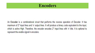
- 1. Encoders
- 15. Bus and Memory transfer ❖ A typical digital computer has many registers, and paths must be provided to transfer information from one register to another. ❖ The number of wires will be excessive if separate lines are used between each register and all other registers in the system. ❖ A more efficient scheme for transferring information between registers in a multiple-register configuration is a common bus system.
- 17. Discussions • One way of constructing a common bus system is with multiplexers. The multiplexers select the source register whose binary information is then placed on the bus. • The construction of a bus system for four registers is shown in figure. • Each register has four bits, numbered 0 through 3. The bus consists of four 4 x 1 multiplexers each having four data inputs, 0 through 3, and two selection inputs, S1 and S0. • In order not to complicate the diagram with 16 lines crossing each other, we use labels to show the connections from the outputs of the registers to the inputs of the multiplexers.
- 18. Discussions • For example, output 1 of register A is connected to input 0 of MUX 1 because this input is labeled A1. • The diagram shows that the bits in the same significant position in each register are connected to the data inputs of one multiplexer to form one line of the bus. • Thus MUX 0 multiplexes the four 0 bits of the registers, MUX 1 multiplexes the four 1 bits of the registers, and similarly for the other two bits.
- 19. Discussions • The two selection lines S1 and S0 are connected to the selection inputs of all four multiplexers. • The selection lines choose the four bits of one register and transfer them into the four-line common bus. When S1S0 = 00, the 0 data inputs of all four multiplexers are selected and applied to the outputs that form the bus. • This causes the bus lines to receive the content of register A since the outputs of this register are connected to the 0 data inputs of the multiplexers. • Similarly, register B is selected if S1S0 = 01, and so on. Table 4-2 shows the register that is selected by the bus for each of the four possible binary value of the selection lines.
- 20. Discussions
- 21. Bus and Memory transfer
- 22. Bus and Memory transfer
- 24. Discussions • The transfer of information from a bus into one of many destination registers can be accomplished by connecting the bus lines to the inputs of all destination registers and activating the load control of the particular destination register selected. • The symbolic statement for a bus transfer may mention the bus or its presence may be implied in the statement. • When the bus is includes in the statement, the register transfer is symbolized as follows:
- 26. Three-State Bus Buffers • A bus system can be constructed with three-state gates. • A three-state gate is a digital circuit that exhibits three states. • Two of the states are signals equivalent to logic 1 and 0 as in a conventional gate. • The third state is a high-impedance state. The high-impedance state behaves like an open circuit, which means that the output is disconnected and does not have a logic significance.
- 27. Three-State Bus Buffers • However, the one most commonly used in the design of a bus system is the buffer gate.
- 28. Three-State Bus Buffers • When the control input is equal to 1, the output is enabled and the gate behaves like any conventional buffer, with the output equal to the normal input. • When the control input is 0, the output is disabled and the gate goes to a high-impedance state, regardless of the value in the normal input.
- 30. Bus line with three state-buffers. *When E=1 and S0 and S1=00 Then 0 output of decoder will be=1 *1st buffer will be active- due to that A0 will be output. *Similarly- S0 and S1=11 then *4th buffer will be active-due to that D0 will be output.
- 31. Three-State Bus Buffers • One way to ensure that no more than one control input is active at any given time is to use a decoder. • When the enable input of the decoder is 0, all of its four outputs are 0, and the bus line is in a high-impedance state because all four buffers are disabled. • When the enable input is active, one of the three-state buffers will be active, depending on the binary value in the select inputs of the decoder.
- 32. Three-State Bus Buffers • One way to ensure that no more than one control input is active at any given time is to use a decoder. • When the enable input of the decoder is 0, all of its four outputs are 0, and the bus line is in a high-impedance state because all four buffers are disabled. • When the enable input is active, one of the three-state buffers will be active, depending on the binary value in the select inputs of the decoder.
- 33. Memory Transfer • The transfer of information from a memory word to the outside environment is called a read operation. • The transfer of new information to be stored into the memory is called a write operation. • A memory word will be symbolized by the letter M . The particular memory word among the many available is selected by the memory address during the transfer. • It is necessary to specify the address of M when writing memory transfer operations. This will be done by enclosing the address in square brackets following the letter M . • Memory stores binary information in groups of bits called as words.
- 34. Memory Transfer
- 37. Adder A half adder is a type of adder, an electronic circuit that performs the addition of numbers. The half adder is able to add two single binary digits and provide the output plus a carry value. It has two inputs, called A and B, and two outputs S (sum) and C (carry). The common representation uses a XOR logic gate and an AND logic gate.
- 39. Adder x y z
- 40. Subtractor
- 41. Subtractor
- 42. Subtractor
- 44. The content of R1 , after the execution of the microoperation, is equal to the bit-by-bit exclusive-OR operation on pairs of bits in R2 and previous values of Rl .
- 45. Special symbols will be adopted for the logic microoperations OR, AND, and complement, to distinguish them from the corresponding symbols used to express Boolean functions. The symbol V will be used to denote an OR microoperation and the symbol to denote an AND microoperation.