SlideShare a Scribd company logo
1 of 127
CPU-Programming Input and Output
 Input and output devices have analog or non-electronic
component. Ex: a disk drive has a rotating disk and analog
read/write electronics but the data are stored in digital format
40
CPU-Programming Input and Output
 The interface between the CPU and the device’s internals is a set
of registers.
 Data registers hold values that are treated as data by the device,
such as the data read or written by a disk.
 Status registers provide information about the device’s
operation, such as whether
Read only registers.
the current transaction has completed.
41
Application Example-8251 UART
 used for serial communications
 UART is programmable for a variety of transmission and reception
parameters
 Start bit (a 0) allows the receiver to recognize the start of a new
character
Stop bit (a 1) indicates the end of transmission of data
42
Application Example-8251 UART
 Baud rate= No of bits transmitted or received/sec
 The parameters for the serial communications are,
 the baud rate
 the number of bits per character (5 through 8)
 whether parity is to be included and whether it is even or odd
 the length of a stop bit (1, 1.5 or 2 bits)
 UART includes one 8-bit register that buffers characters between
the UART and the CPU bus
43
Application Example-8251 UART
 Transmitter Ready output- indicates that the transmitter is
ready to send
 Transmitter Empty signal goes high when the UART has no
characters to send
 Receiver Ready pin goes high when the UART has a character
ready to be read by the CPU
44
Input and Output Primitives
 Microprocessors can provide programming support for input and
output in two ways: I/O instructions (in and out instructions in
Intel x86- These instructions provide a separate address space for
I/O devices-Ported I/O) and memory-mapped I/O (provides
addresses for the registers in each I/O device)
 Programs use the CPU’s normal read and write instructions to
communicate with the devices
45
Input and Output Primitives
46
Memory-mapped I/O in Assembly
47
Memory-mapped I/O in C
 Traditional names for functions that read and write arbitrary
memory locations are peek and poke
 To read a device register we can write,
48
Memory-mapped I/O in C
To write to the status register,
 These functions can, of course, be used to read
memory locations, not just devices
and write arbitrary
49
Busy-Wait I/O
 I/O devices are much slower than the CPU and may require many
cycles to complete an operation.
 CPU must wait for one operation to complete before starting the
next one. CPU does this by checking
device.
the status registers of an I/O
 Asking an I/O device whether it is finished by reading its status
register is often called polling.
50
Busy-Wait I/O Programming
 To write a sequence of characters to an output device. Device has
two registers: one for the character to be written and a status
register.
 The status register value is 1 when the device is busy writing and
0 when the transaction has completed.
51
Busy-Wait I/O Programming
52
Interrupts
 Busy-wait I/O is extremely inefficient- the CPU does nothing
but test the device status while the I/O transaction is in progress. In
many cases, the CPU could do useful work in parallel with the
transaction, such as,
I/O
 computation, as in determining the next output to send to
device or processing the last input received
the
 control of other I/O devices
 Interrupt mechanism allows devices to signal the CPU and to force
execution of a particular piece of code
53
Interrupts
 When an interrupt occurs, the program counters value is changed
to point to an interrupt handler routine (also commonly known as
a device driver- that takes care of the device like writing the next
data, reading data and so on).
 The interrupt mechanism of
interruption so that the CPU
interrupted.
course saves the value of the PC at the
can return to the program that was
 Interrupts allow the flow of control in the CPU to change easily
between different contexts, such as a foreground computation and
multiple I/O devices.
54
Interrupt Mechanism
55
Interrupt Mechanism
 Priority based interrupt service- Ex: a program that talks to both a
high-speed disk drive and a low-speed keyboard should be designed
to finish a disk transaction before handling a keyboard interrupt.
 The program that runs when no interrupt is being handled is often
called the foreground program.
56
Interrupt Mechanism-Example
Copying characters from input to output devices with basic
interrupts
57
Interrupt Mechanism-Example
Copying characters from input to output devices with basic
interrupts
58
Interrupt Mechanism-I/O Buffers
Copying characters from input
program
to output devices with
writes
interrupts and buffers-
independently
The performs reads and
 Queue is empty
 Add characters to the tail when an input is received and take
characters from the head when we are ready for output
 When the first character is read, the tail is incremented after the
character is added to the queue, leaving the buffer and pointers
59
Interrupt Mechanism-I/O Buffers
 When the buffer is full, we leave one character in the buffer
unused.
 When the output goes past the end of io_buf,
60
Interrupt Mechanism-I/O Buffers
≤
61
Interrupt Mechanism-I/O Buffers
62
Interrupt Mechanism-I/O Buffers
63
Interrupt Mechanism-I/O Buffers
64
Interrupt Mechanism-I/O Buffers-UML Sequence
Diagram
65
Interrupt Mechanism-I/O Buffers-UML Sequence
Diagram
 The CPU implements interrupts by checking the interrupt request
line at the beginning of execution of every instruction. If an interrupt
request has been asserted, the CPU does not fetch the instruction
pointed to by the PC.
 Instead the CPU sets the PC to a predefined location, which is the
beginning of the interrupt handling routine.
66
Interrupt Priorities and Vectors
 Interrupt priorities allow the CPU to recognize some interrupts as
more important than others (Ex: L1-High priority)
 Interrupt vectors
handler
allow the interrupting device to specify its
67
Interrupt Priorities and Vectors
 Priority mechanism must ensure that a lower priority interrupt
does not occur when a higher-priority interrupt is being handled.
The decision process is known as masking.
 When an interrupt is acknowledged, the CPU stores in an internal
register the priority level of that interrupt.
 When a subsequent interrupt is received, its priority is checked
against the priority register; the new request is acknowledged only if
it has higher priority than the currently pending interrupt.
 The highest priority interrupt is normally called the non-maskable
interrupt (NMI) (Ex: caused by power failures) 68
Interrupt Priorities and Vectors
 Interrupts with same priority can be serviced by polling
mechanism
69
Interrupt Vectors
 Vector number is stored in device, not the CPU
There is no fixed relationship between vector numbers and
interrupt handlers.
70
Example: I/O with Prioritized Interrupts
A- Highest
C- Lowest
71
Interrupt overhead
 Once a device requests an interrupt, some steps are performed by
the CPU, some by the device, and others by software.
 CPU: Checks for pending interrupts at the beginning of an
instruction. It answers the highest priority interrupt, which has a
higher priority than that given in the interrupt priority register.
 Device: Receives the acknowledgement from CPU and sends the
CPU its interrupt vector.
 CPU: Looks up the device handler address in the interrupt vector
table using the vector as an index. Current value of the PC, internal
CPU state and general purpose registers are saved. 72
Interrupt overhead
 Software: The device driver may save additional CPU state. It then
performs the required operations on the device. It then restores any
saved state and executes the interrupt return instruction.
 CPU: The interrupt return instruction restores the PC and other
automatically
interrupted.
saved states to return execution to the code that was
73
Interrupt overhead
 Execution time required for the code that
devices- Execution time overhead
talks directly to the
Interrupt causes a change in the program counter, it incurs a
branch penalty. In addition, if the interrupt automatically stores
CPU registers, that action requires extra cycles, even if the state is
not modified by the interrupt handler.
 The interrupt requires extra cycles to acknowledge the interrupt
and obtain the vector from the device.
 Interrupt handler will save and restore CPU registers that were
not automatically saved by the interrupt. 74
Interrupt overhead
 The interrupt return instruction incurs a branch penalty as well
as the time required to restore the automatically saved state.
75
Interrupts in ARM
 ARM7 supports two types of interrupts: fast interrupt requests
(FIQs) and interrupt requests (IRQs).
 An FIQ takes priority over an IRQ.
 The interrupt table is always kept in the bottom memory
addresses, starting at location 0.
 The entries in the
appropriate handler.
table typically contain subroutine calls to the
76
Interrupts in ARM
ARM7 performs the following steps when responding to an
interrupt.
 saves the appropriate value of the PC to be used to return.
 copies the CPSR into a saved program status register (SPSR).
 forces bits in the CPSR to note the interrupt, and
 forces the PC to the appropriate interrupt vector.
When leaving the interrupt handler, the handler should:
 restore the proper PC value.
 restore the CPSR from the SPSR, and
 clear interrupt disable flags. 77
Interrupts in ARM
The worst case latency to
components:
respond to an interrupt includes the
 two cycles to synchronize the external request.
 up to 20 cycles to complete the current instruction.
 three cycles for data abort, and
 two cycles to enter the interrupt handling state.
This adds up to 27 clock cycles. The best case latency is four clock
cycle.
78
Supervisor mode
 Complex systems are often implemented as several programs
that communicate with each other. These programs may run under
the command of an operating system.
 It may be desirable to provide hardware checks to ensure that the
programs do not interfere with each other- Additional level of safety.
 Normal programs run in user mode.
 The supervisor mode has privileges that user modes do not.
Control of the memory management unit (MMU) is typically
reserved for supervisor mode to avoid inadvertent changes in the
memory management registers. 79
Supervisor mode in ARM
 The ARM instruction that puts the CPU in supervisor mode is
called SWI.
SWI CODE_1
 SWI causes the CPU to go into supervisor mode and sets the PC to
0x08.
 The argument to SWI is a 24-bit immediate value that is passed
on to the supervisor
various services from
mode code; it allows the program to request
the supervisor mode.
80
Supervisor mode in ARM
 In supervisor mode, the bottom 5 bits of the CPSR are all set to 1.
2
4
8 7 6 5
4
31 30 29 28 27
I I
0
I
J Reserved
Field I
I IStatus Extention Field Control Field
Flag Field
81
Mode bits M[4:0}
OblOOOO User
Oblllll System
OblOOOl AQ
Ob10010 IRQ
Ob10011 SVC(Supervisor)
Ob10111 Abort
Ob11011 Undefined
Control bits
I 1: disables IRQ
F 1: disables AQ
T 1: Thumb,0: ARM
Flag
Field
N Negative result from ALU
z Zero result from ALU
c ALU operation caused Carry
v ALU operation overflowed
Q ALU operation saturated
J Java Byte Code Execution
Supervisor mode in ARM
 The old value of the CPSR just before the SWI is stored in a
register called the saved program status register (SPSR).
Several SPSRs for different modes, the supervisor SPSR is referred
to as SPSR_svc
 To return from the supervisor mode, the supervisor restores the
PC from register r14 and restores the CPSR from the SPSR_svc.
82
Exceptions
 An exception is an internally detected
zero.
error. Ex: division by
 The CPU can more efficiently check the divisors value during
execution. Since the time at which a zero divisor will be found is not
known in advance, this event is similar to an interrupt except that it
is generated inside the CPU. The exception mechanism provides a
way for the program to react to such unexpected events.
 Exceptions are similar to interrupts, however exceptions are
generated internally.
83
Exceptions
 Exceptions in general require both prioritization and vectoring.
 Exceptions must be prioritized because a single operation may
generate more than one exception. Ex: an illegal operand and an
illegal memory access.
 The priority of exceptions is usually fixed by the CPU architecture.
 Vectoring provides a way for the user to specify the handler for
the exception condition.
 The vector number for an exception is usually predefined by the
architecture; it is used to index into a table of exception handlers.
84
Traps
 A trap also known as a software interrupt, is an instruction that
explicitly generates an exception condition.
 The most common use of a trap is to enter supervisor mode.
 The entry into supervisor mode must be controlled to maintain
security.
 The ARM provides the SWI interrupt for software interrupts. This
instruction causes the CPU to enter supervisor mode. An opcode is
embedded in the instruction that can be read by the handler.
85
Co-Processors
 Co-processors are attached to the CPU and implement some of
the instructions. Ex: floating point arithmetic in Intel architecture.
 To support co-processor, certain opcodes must be reserved in the
instruction set for co-processor operations.
 Because it executes instructions, a co-processor must be tightly
coupled to the CPU.
 When the CPU receives a co-processor instruction, the CPU must
activate the co-processor and pass it the relevant instruction.
 Co-processor instructions can load and store co-processor
registers or can perform internal operations. 86
Co-Processors
 The CPU can suspend execution to wait for the co-processor
superscalar approach
instruction to finish; it can also take a more
while
and continue executing instructions waiting for the co-
processor to finish.
 A CPU may, of course, receive co-processor instructions even when
there is no co-processor attached. Most architectures use illegal
instruction traps to handle these situations.
 The trap handler can detect the co-processor instruction and
execute it in software
instructions in software
on the main CPU. Emulating co-processor
is slower but provides compatibility.
87
Co-Processors in ARM
 Supports up to 16 co-processors.
 Co-processors are able to perform load and store operations on
their own registers.
 They can also move data between the co-processor registers
and main ARM registers.
 Ex: Floating point co-processor- It provides eight 80-bit floating
point data registers and floating point status registers.
88
Memory System Mechanisms
 Modern Microprocessor Units (MMU)- do more than just read and
write a monolithic memory.
Microprocessor clock rates
speeds.
are increasing rapidly than memory
 Modern Microprocessor Units (MMU) perform address
translations that provide
physical memory.
a larger virtual memory space in a small
89
Caches
 Caches are widely used to speed up memory system performance.
 It speeds up average memory access time when properly used. Hit
(data available in Cache memory) and Miss (data not available in
Cache memory).
 A cache is a small, fast memory that holds copies of some of the
contents of main memory. Because the cache is fast, it provides
higher-speed access for the CPU; but since it is small, not all the
requests can be satisfied by the cache, forcing the system to wait for
the slower main memory.
90
Caches
 Caching makes sense when the CPU is using only a relatively
small set of memory locations at any one time; the set of active
locations is often called the working set.
 Ex: Data read from memory
91
Caches in the Memory System
 Classification of cache miss
A Compulsory Miss ( Cold miss) occurs the first time a location is used.
A Capacity Miss is caused by a too-large working set, and
A Conflict Miss
cache.
happens when two locations map to the same location in the
92
Memory System Performance
where h – hit rate (probability that a given memory
the cache)
location is in
1- h is the miss rate (probability that location is not in the cache)
tav is the average memory access rate
tcache
tmain
is the access time of the cache
is the main memory access time
93
Memory System Performance
 Best case memory access time (ignoring cache controller
overhead) is tcache. Few nano seconds.
 Worst case access time is tmain. 50-60 ns.
94
Multi-level Cache: Two – level cache system
 L1 cache- first level (closest to the CPU).
 L2 cache- second level cache (feeds the first level cache): much
larger but is also slower.
95
Two – level cache system
where L1 – first-level cache
L2 – second-level cache
h1 – first-level hit rate
h2 is the rate at which access
the first- level cache
hit the second level cache but not
tav is the average memory access rate
tmain is the main memory access time
96
Data replacement system in cache
 As the program working set changes, we expect locations to be
removed from the cache to make way for new locations.
 One possible replacement policy is least recently used (LRU), that
is, throw out the block that has been used farthest in the past. Add
relatively small amount of hardware to the cache to keep track of the
time since last access of each block.
 Another policy is random
hardware to implement.
replacement, which requires even less
97
Direct - Mapped Cache
 The cache consists of cache blocks, each of which includes a tag to
show which memory location is represented by this block, a data
field holding the contents of that memory, and a
valid.
valid tag to show
whether the contents of this cache block are
98
Direct - Mapped Cache
 An address is divided into three sections.
 Index – used to select which cache block to check
 Address tag is compared with cache tag selected by the index. If it matches,
that block includes the desired memory location.
 If the length of the data field is longer than the minimum addressable unit,
then the lowest bits of the address are used as an offset to select the
value from the data field.
required
 If the access is a hit, the data value is read from the cache.
99
Direct - Mapped Cache
Writing the data in cache needs updation of main memory too.
Write – Through scheme (every write changes both the cache and the
corresponding main memory location- usually through the write buffer). This
method ensures that the cache and main memory are consistent, but may
generate some additional main memory traffic.
n
Write – Back Policy (We write only when we remove
written
a location from the
cache, we eliminate the writes
it is removed from cache)
when a location is several times before
100
Direct - Mapped Cache
 Advantage: Is fast and relatively low cost.
 Disadvantage: If two popular locations in a program happen to
map onto
cache.
the same block, we will not gain the full benefits of the
101
Set - Associative Cache
 A set-associative cache is characterized by the number of banks or
ways it uses, giving an n-way set associative cache.
102
Set - Associative Cache
 A set is formed by all the blocks (one for each bank) that shares the
same index. Each set is implemented with a direct-mapped cache.
 A cache request is broadcast to all the banks simultaneously.
 If any of the sets has the location, the cache reports a hit.
103
Set - Associative Cache
 Therefore, we can simultaneously cache several locations that
happen to map onto the same cache block.
 It incurs a little extra overhead and is slightly slower than the
direct mapped cache, but has higher hit rates.
104
Direct mapped vs Set - Associative Cache
Example:
2 bits of the address as tag.
 Direct mapped cache with four blocks
 two way set associative cache with four sets
 We use Least recently used (LRU) replacement to make it easy to
compare the two caches.
105
Direct mapped vs. Set - Associative Cache
106
Direct mapped vs. Set - Associative Cache
Direct mapping- 001, 010, 011, 100, 101 and 111
107
Direct mapped vs. Set - Associative Cache
Set-Associative mapping- 001, 010, 011, 100, 101 and 111
Four set-two way associative mapping
108
Caches in ARM
 A cache that holds both instructions and data is called a unified
cache.
 ARM 600 includes a 4 KB, 64 way unified instruction/data cache.
 The Strong ARM uses a 16 KB, 32-way instruction cache with a 32-
byte
data
block
cache
and a 16 KB, 32 way data cache with a 32-byte block; the
uses a write-back strategy.
109
Memory Management Units and Address
Translation
 A memory management unit (MMU) translates addresses between
the CPU and physical memory- Memory mapping (addresses are
mapped from a logical space into a physical space)
 When memory became cheap enough that physical memory could
be larger than the address space defined by the instruction, MMUs
allowed software to manage multiple programs in a single physical
memory, each with its own address space- Virtual addressing.
 Use physical DRAM (Main memory) as a cache for the secondary
storage (Flash, disk)
110
Memory Management Units and Address
Translation
 MMU accepts logical addresses from the CPU. Logical addresses
refer to the program’s abstract address space but do not correspond
to actual RAM locations.
 The MMU translates them from tables to physical addresses that
do correspond to RAM.
111
Memory Management Units and Address
Translation
 By changing the MMU’s tables. you can change the physical
location at which the program resides without modifying the
program’s code or data.
 In a virtual memory system, the
addresses are actually resident in
MMU keeps track of which logical
main memory; those that do not
reside in main memory are kept on the secondary storage device.
 When the CPU requests an address that is not in main memory, the
MMU generates an exception called a page fault. The handler for this
exception executes code that reads the requested location from the
secondary storage device into main memory.
112
Memory Management Units and Address
Translation
 The program that generated the page fault is restarted by the
handler only after,
The required memory has been read back into main memory, and
The MMU tables have been updated to reflect the changes.
 The displaced memory is copied into secondary storage before the
requested location is read in. As with caches, LRU is a good
replacement policy.
113
Address Translation
 Two styles of Address Translation are,
Segmented
Paged
 Two can also be combined to form a segmented, paged addressing
scheme.
 Segmenting is designed to support a large, arbitrarily sized region
of memory, while pages describe small, equally sized regions.
114
Address Translation-Segments and Pages
115
Address Translation-Segments and Pages
 A segment is usually described by its start address and size,
allowing different segments to be of different sizes.
 Pages are of uniform size, which simplifies the hardware required
for address translation.
 A segmented, paged scheme is created by dividing each segment
into pages and using two steps for address translation.
 Paging introduces the possibility of fragmentation as program
pages are scattered around physical memory.
116
Address Translation for a segment
117
Address Translation for a segment
118
Address Translation for a segment
119
Address Translation for a segment
 The MMU would maintain a segment register that describes the
the
currently active segment. This register would point to the base
current segment.
of
 The address extracted from an instruction (or from any
source for addresses, such as a register) would be used as the
for the address.
other
offset
The physical address is formed by adding the segment base
offset.
to the
 The segment register may also include the segment size and
compare the offset to the allowed size. 120
Address Translation for a page
121
Address Translation for a page
 The logical address is divided into two sections, including a page
number and an offset.
The page number is used as an index into a page table, which
stores the physical address for the start of each page.
Since all pages have the same size, the MMU simply needs to
concatenate the top bits of the page starting address with the
bits from the page offset to form the physical address.
bottom
Pages are small, typically between 512 bytes and 4 KB.
The page table (kept in main memory- requires an memory
is large for an architecture with a large address space.
access)
122
Page table organization
 Page table may be organized in several ways,
 Flat table (The table is indexed by the page number and each entry holds the
page descriptor)
 Tree structured ( The root entry of the tree holds pointers to pointer tables
at the next level of the tree; each pointer table is indexed by a part of the page
number. We eventually (after three levels, in this case) arrive at a descriptor
table that includes the page descriptor we are interested in.)
 A tree-structured page table incurs some overhead for the
pointers, but it allows us to build a partially populated tree. If some
part of the address space
part of the tree that covers
is
it.
not used, we do not need to build the
123
Page table organization
124
Address Translation
The efficiency of paged address translation may be increased by
caching page translation information.
 A cache for address translation is known as a translation lookaside
buffer (TLB).
 The MMU reads the TLB to check whether a page number is
currently in the TLB cache
reading from memory.
and, if so, uses that value rather than
125
Address Translation-TLB
126
Address Translation-TLB
127
Address Translation-TLB
 When a Virtual Address is accessed, and then looked up, the TLB
Cache is checked first to see if the Virtual-Physical Address mapping
is present and if so then a TLB Hit occurs.
 On the other hand, if the address isn't present, then a TLB Miss
occurs and the MMU is forced to execute a Page Walk which is the
process of looking through the Page Tables.
 Once, the Page Walk has completed and the physical address is
found, then this information is loaded into the TLB Cache.
 If Page Walk is unsuccessful, then a Page Fault is raised, and the
Virtual to Physical Address Mapping is created in the Page Table.
128
Address Translation
Criteria required for segmenting and paging for virtual memory
At minimum, a present bit is necessary to show whether the logical segment
or page is currently in physical memory.
A dirty bit shows whether the page/segment has been written to. This bit is
maintained by the MMU, since it knows about every write performed by the
CPU.
Permission bits are often used. Some pages/ segments may be readable but
not writable. If the CPU support modes, pages/ segments may be accessible by
the supervisor but not in user mode.
 A data or instruction cache may operate either on logical or
physical addresses, depending on where it is positioned relative to
the MMU. 129
MMU in ARM
 A MMU is an optional part of the ARM architecture.
The ARM MMU supports both virtual address translation and
memory protection; the architecture requires that the MMU be
implemented when cache or write buffers are implemented.
The ARM MMU supports the following
address translation:
Section (1 MB block of memory)
types of memory regions for
Large page (64 KB)
Small Page (4 KB)
130
ARM MMU Address translation
An address is marked as section mapped or page mapped.
 A two-level scheme is used to translate addresses.
 The first-level table, which is pointed to by the Translation Table
Base register, holds descriptors for section translation and pointers
to the second-level tables.
 The second-level tables describe the translation of both large and
small pages.
The first- and second-level pages also contain access control bits
for virtual memory and protection.
131
ARM Two- stage address translation
- Virtual address
Second-level Index Offset
Second-level table
132
... First-level
Index
First-level descriptor I
Concatenate
First-level table
Second-level descriptor
Concatenate
Physical address
TranslaUon Table
Base resister
CPU Performance-Pipelining
 Modern CPUs are designed as pipelined machines in which several
instructions are executed in parallel.
 Pipelining greatly increases the efficiency of the CPU.
 Branch and go to statements affect the performance of pipelining
in CPU.
133
ARM 7 Pipelining
 Three – stage pipelining.
Fetch – instruction fetched from memory.
Decode – instruction’s opcode and operands
determine the function to perform.
are decoded to
Execute – the decoded instruction is executed.
Each stage requires one clock cycle per instruction
Latency- 3 clock cycles required for single instruction
without pipelining
execution
Pipelining has a throughput of one instruction per cycle.
134
Pipelined execution of ARM Instructions
Extended execution is when an instruction is too complex to
complete the execution phase in a single cycle. Example: Multiple
load instruction (ldmia r0,[r2,r3])
135
Pipelined execution of multicycle ARM Instruction
Data stall in the execution of a sequence of instructions.
 In multiphase execution, the decode stage is also occupied, since it
must continue to remember the decoded instruction.
136
Pipelined execution of a branch in ARM
 Branches also introduce control stall delays into the pipeline,
commonly referred to as the branch penalty.
 The CPU uses the two cycles between starting to fetch the branch
target and starting to execute that instruction.
137
Caching
Although caches are invisible in the programming model, they have
a profound effect on performance.
 The extra time required to access a memory location not in the
cache is often called the cache miss penalty.
Data may not be available in cache due to several reasons:
At a compulsory miss, the location has not been referenced before.
At a conflict miss, two particular memory locations are fighting for the same
cache line.
At a capacity miss, the program’s working set is simply too large for the
cache.
138
Caching
 When we have several programs running concurrently on the CPU,
we can have very dramatic changes in the cache contents.
139
CPU Power Consumption
 Power consumption is as important as execution time.
Power- energy consumption per unit time.
 Heat generation depends on power consumption.
 Battery life depends on energy consumption.
 Today, virtually all digital systems are built with complementary
metal oxide semiconductor (CMOS) circuitry.
 The basic sources of CMOS power consumption are:
Voltage Drops (dynamic power consumption ∝ square of power supply
voltage (V2)). Reducing the power supply voltage to the lowest that provide
the required performance and also by using additional parallel hardware.
140
CPU Power Consumption
Toggling- A CMOS circuit uses most of its power when it is changing its output
value. By reducing the speed at which the circuit operates, we can reduce its
power consumption. Eliminating unnecessary glitches at the circuit input and
output eliminates unnecessary power consumption.
Leakage- Even when a CMOS circuit is not active, some charge leaks out of the
circuit nodes through the substrate. The only way to eliminate leakage current
is to remove the power supply but it
for rebooting the system.
usually takes a significant amount of time
141
Power Saving Strategies used in CMOS CPUs
CPUs can be used at reduced voltage levels. by reducing
supply causing power consumption reduction.
power
CPU can be operated at a lower clock frequency to reduce
consumption.
power
CPU may internally disable certain function
function,
units that are not
required for the currently executing thereby reducing
energy consumption.
Some CPUs allow parts of the CPU to be totally disconnected from
the power supply to eliminate leakage currents.
142
Power management features provided by CPUs
Static power management mechanism-is invoked by the user but
does not otherwise depend on CPU activities. Example: power down
mode intended to save energy. Instruction based mode activation.
Power-down modes typically end upon receipt of an interrupt or
other events.
Dynamic power management mechanism takes actions to control
power based upon the dynamic activity in the CPU when the
instructions being executed do not need them.
143
Power saving modes of Strong ARM SA-1100
Run mode - highest power consumption.
Idle Mode – saves power by saving the CPU Clock.
Sleep mode – shuts off most of the chip’s activity
three orders of magnitude of power consumption.
and saves about
Time taken
second.
to reenter run mode from sleep is over a tenth of a
144
Power saving modes of Strong ARM SA-1100
145
Design Example: Data Compressor
Data compressor takes in data with a constant number of bits per
data
data
element and puts out a compressed data stream in which the
is encoded in variable length symbols.
146
Requirements and Algorithm
Huffman coding technique is used for data compression.
 The data compressor takes in a sequence of input symbols and
then produces a stream of output symbols.
 Assume input symbols of one byte in length.
 The output symbols are variable length, so we have to choose a
format in which to deliver the output data. (code, length).
 Bit by bit delivery is also too slow.
 Data compressor is going to pack the coded symbols into an array.
147
Huffman coding for text compression
Text compression algorithms aim at statistical reductions in the
volume of data.
 Huffman coding makes use of information on the frequency of
characters to assign variable length codes to characters.
 Shorter bit sequences are used to identify more frequent
characters, then the length of the total sequence will be reduced.
 To decode the incoming bit string, the code characters must have
unique prefixes.
148
Huffman coding for text compression
Example: Assume that these characters have the following
probabilities P of appearance in a message.
 Bottom up approach
149
Huffman coding for text compression
150
Huffman coding for text compression
Reading the codes off the tree from the root to the leaves, we
obtain the following coding of the characters.
151
Data compressor- Requirement list
152
Data compressor- Specification
For a fully functional system (dynamic),
 We have to be able to provide the compressor with a new
symbol table.
 We should be able to flush the symbol buffer to cause the
system to release all pending symbols that have been partially
packed. We may want to do this when we change the symbol
table or in the middle of an encoding session to keep the
transmitter busy.
153
Data compressor- Specification
154
Data compressor- Specification
The class’s buffer and current-bit behaviors keep track
of the encoding.
of the state
 The table attribute provides the current symbol table.
 The class has three methods as follows:
 Encode performs the basic encoding function. It takes in a 1-byte
input symbol and returns two values: a boolean showing whether it
is returning a full buffer.
 New symbol-table installs a new symbol table into the object and
throws away the current contents of the internal buffer.
155
Data compressor- Specification
 Flush returns the current state of the buffer, including the number
of valid bits in the buffer.
156
Data compressor- Specification
157
Data compressor- Specification
158
Data compressor- Specification
 The data buffer will be used to hold both packed and unpacked
symbols (such as in symbol table). It defines the buffer itself and the
length of the buffer.
 The insert function packs a new symbol into the upper bits of the
buffer; it also puts the remaining bits in
buffer is overflowed.
a new buffer if the current
 The symbol-table class indexes the
symbol.
encoded version of each
 The load function is used to create a new symbol table.
159
Data compressor- Specification
160
Data compressor- Testing
161

More Related Content

Similar to UNIT 2.pptx

Microprocessor Basics 8085 Ch-1
Microprocessor Basics 8085 Ch-1Microprocessor Basics 8085 Ch-1
Microprocessor Basics 8085 Ch-1Neelam Kapoor
 
Nvidia tegra K1 Presentation
Nvidia tegra K1 PresentationNvidia tegra K1 Presentation
Nvidia tegra K1 PresentationANURAG SEKHSARIA
 
COA-Unit5-ppt2.pptx
COA-Unit5-ppt2.pptxCOA-Unit5-ppt2.pptx
COA-Unit5-ppt2.pptxRuhul Amin
 
IO and file systems
IO and file systems IO and file systems
IO and file systems EktaVaswani2
 
Iosystemspre final-160922112930
Iosystemspre final-160922112930Iosystemspre final-160922112930
Iosystemspre final-160922112930marangburu42
 
Introduction to-microprocessor
Introduction to-microprocessorIntroduction to-microprocessor
Introduction to-microprocessorankitnav1
 
Introduction to-microprocessor
Introduction to-microprocessorIntroduction to-microprocessor
Introduction to-microprocessorankitnav1
 
The central processing unit by group 5 2015
The central processing unit by group 5 2015The central processing unit by group 5 2015
The central processing unit by group 5 2015Tendai Karuma
 
Computer Organisation & Architecture (chapter 1)
Computer Organisation & Architecture (chapter 1) Computer Organisation & Architecture (chapter 1)
Computer Organisation & Architecture (chapter 1) Subhasis Dash
 
Processor Management
Processor ManagementProcessor Management
Processor ManagementSumit kumar
 
Unit2 p1 io organization-97-2003
Unit2 p1 io organization-97-2003Unit2 p1 io organization-97-2003
Unit2 p1 io organization-97-2003Swathi Veeradhi
 
Material Architecture and organization of computer
Material Architecture and organization of computerMaterial Architecture and organization of computer
Material Architecture and organization of computerferoza rosalina
 
Introduction to Operating Systems
 Introduction to Operating Systems Introduction to Operating Systems
Introduction to Operating SystemsJérôme Kehrli
 
Basic computer in detail with pictures created by creativeness
Basic computer in detail with pictures created by creativenessBasic computer in detail with pictures created by creativeness
Basic computer in detail with pictures created by creativenessAparna Samal
 
Computer Organization and Architechuture basics
Computer Organization and Architechuture basicsComputer Organization and Architechuture basics
Computer Organization and Architechuture basicsLucky Sithole
 
L-1 BCE computer fundamentals final kirti.ppt
L-1 BCE computer fundamentals final kirti.pptL-1 BCE computer fundamentals final kirti.ppt
L-1 BCE computer fundamentals final kirti.pptKirti Verma
 

Similar to UNIT 2.pptx (20)

Microprocessor Basics 8085 Ch-1
Microprocessor Basics 8085 Ch-1Microprocessor Basics 8085 Ch-1
Microprocessor Basics 8085 Ch-1
 
Nvidia tegra K1 Presentation
Nvidia tegra K1 PresentationNvidia tegra K1 Presentation
Nvidia tegra K1 Presentation
 
COA-Unit5-ppt2.pptx
COA-Unit5-ppt2.pptxCOA-Unit5-ppt2.pptx
COA-Unit5-ppt2.pptx
 
IO and file systems
IO and file systems IO and file systems
IO and file systems
 
Iosystemspre final-160922112930
Iosystemspre final-160922112930Iosystemspre final-160922112930
Iosystemspre final-160922112930
 
Introduction to-microprocessor
Introduction to-microprocessorIntroduction to-microprocessor
Introduction to-microprocessor
 
Introduction to-microprocessor
Introduction to-microprocessorIntroduction to-microprocessor
Introduction to-microprocessor
 
The central processing unit by group 5 2015
The central processing unit by group 5 2015The central processing unit by group 5 2015
The central processing unit by group 5 2015
 
IO_ORGANIZATION.pdf
IO_ORGANIZATION.pdfIO_ORGANIZATION.pdf
IO_ORGANIZATION.pdf
 
Computer Organisation & Architecture (chapter 1)
Computer Organisation & Architecture (chapter 1) Computer Organisation & Architecture (chapter 1)
Computer Organisation & Architecture (chapter 1)
 
Processor Management
Processor ManagementProcessor Management
Processor Management
 
Unit2 p1 io organization-97-2003
Unit2 p1 io organization-97-2003Unit2 p1 io organization-97-2003
Unit2 p1 io organization-97-2003
 
Material Architecture and organization of computer
Material Architecture and organization of computerMaterial Architecture and organization of computer
Material Architecture and organization of computer
 
Introduction to Operating Systems
 Introduction to Operating Systems Introduction to Operating Systems
Introduction to Operating Systems
 
Basic computer in detail with pictures created by creativeness
Basic computer in detail with pictures created by creativenessBasic computer in detail with pictures created by creativeness
Basic computer in detail with pictures created by creativeness
 
Pentium processor
Pentium processorPentium processor
Pentium processor
 
CAO.pptx
CAO.pptxCAO.pptx
CAO.pptx
 
Interrupts
InterruptsInterrupts
Interrupts
 
Computer Organization and Architechuture basics
Computer Organization and Architechuture basicsComputer Organization and Architechuture basics
Computer Organization and Architechuture basics
 
L-1 BCE computer fundamentals final kirti.ppt
L-1 BCE computer fundamentals final kirti.pptL-1 BCE computer fundamentals final kirti.ppt
L-1 BCE computer fundamentals final kirti.ppt
 

Recently uploaded

Risk Assessment For Installation of Drainage Pipes.pdf
Risk Assessment For Installation of Drainage Pipes.pdfRisk Assessment For Installation of Drainage Pipes.pdf
Risk Assessment For Installation of Drainage Pipes.pdfROCENODodongVILLACER
 
Decoding Kotlin - Your guide to solving the mysterious in Kotlin.pptx
Decoding Kotlin - Your guide to solving the mysterious in Kotlin.pptxDecoding Kotlin - Your guide to solving the mysterious in Kotlin.pptx
Decoding Kotlin - Your guide to solving the mysterious in Kotlin.pptxJoão Esperancinha
 
GDSC ASEB Gen AI study jams presentation
GDSC ASEB Gen AI study jams presentationGDSC ASEB Gen AI study jams presentation
GDSC ASEB Gen AI study jams presentationGDSCAESB
 
An experimental study in using natural admixture as an alternative for chemic...
An experimental study in using natural admixture as an alternative for chemic...An experimental study in using natural admixture as an alternative for chemic...
An experimental study in using natural admixture as an alternative for chemic...Chandu841456
 
Arduino_CSE ece ppt for working and principal of arduino.ppt
Arduino_CSE ece ppt for working and principal of arduino.pptArduino_CSE ece ppt for working and principal of arduino.ppt
Arduino_CSE ece ppt for working and principal of arduino.pptSAURABHKUMAR892774
 
Heart Disease Prediction using machine learning.pptx
Heart Disease Prediction using machine learning.pptxHeart Disease Prediction using machine learning.pptx
Heart Disease Prediction using machine learning.pptxPoojaBan
 
pipeline in computer architecture design
pipeline in computer architecture  designpipeline in computer architecture  design
pipeline in computer architecture designssuser87fa0c1
 
Call Us ≽ 8377877756 ≼ Call Girls In Shastri Nagar (Delhi)
Call Us ≽ 8377877756 ≼ Call Girls In Shastri Nagar (Delhi)Call Us ≽ 8377877756 ≼ Call Girls In Shastri Nagar (Delhi)
Call Us ≽ 8377877756 ≼ Call Girls In Shastri Nagar (Delhi)dollysharma2066
 
Call Girls Narol 7397865700 Independent Call Girls
Call Girls Narol 7397865700 Independent Call GirlsCall Girls Narol 7397865700 Independent Call Girls
Call Girls Narol 7397865700 Independent Call Girlsssuser7cb4ff
 
Architect Hassan Khalil Portfolio for 2024
Architect Hassan Khalil Portfolio for 2024Architect Hassan Khalil Portfolio for 2024
Architect Hassan Khalil Portfolio for 2024hassan khalil
 
Gurgaon ✡️9711147426✨Call In girls Gurgaon Sector 51 escort service
Gurgaon ✡️9711147426✨Call In girls Gurgaon Sector 51 escort serviceGurgaon ✡️9711147426✨Call In girls Gurgaon Sector 51 escort service
Gurgaon ✡️9711147426✨Call In girls Gurgaon Sector 51 escort servicejennyeacort
 
EduAI - E learning Platform integrated with AI
EduAI - E learning Platform integrated with AIEduAI - E learning Platform integrated with AI
EduAI - E learning Platform integrated with AIkoyaldeepu123
 
Software and Systems Engineering Standards: Verification and Validation of Sy...
Software and Systems Engineering Standards: Verification and Validation of Sy...Software and Systems Engineering Standards: Verification and Validation of Sy...
Software and Systems Engineering Standards: Verification and Validation of Sy...VICTOR MAESTRE RAMIREZ
 
UNIT III ANALOG ELECTRONICS (BASIC ELECTRONICS)
UNIT III ANALOG ELECTRONICS (BASIC ELECTRONICS)UNIT III ANALOG ELECTRONICS (BASIC ELECTRONICS)
UNIT III ANALOG ELECTRONICS (BASIC ELECTRONICS)Dr SOUNDIRARAJ N
 
CCS355 Neural Network & Deep Learning UNIT III notes and Question bank .pdf
CCS355 Neural Network & Deep Learning UNIT III notes and Question bank .pdfCCS355 Neural Network & Deep Learning UNIT III notes and Question bank .pdf
CCS355 Neural Network & Deep Learning UNIT III notes and Question bank .pdfAsst.prof M.Gokilavani
 
Churning of Butter, Factors affecting .
Churning of Butter, Factors affecting  .Churning of Butter, Factors affecting  .
Churning of Butter, Factors affecting .Satyam Kumar
 
Biology for Computer Engineers Course Handout.pptx
Biology for Computer Engineers Course Handout.pptxBiology for Computer Engineers Course Handout.pptx
Biology for Computer Engineers Course Handout.pptxDeepakSakkari2
 

Recently uploaded (20)

Risk Assessment For Installation of Drainage Pipes.pdf
Risk Assessment For Installation of Drainage Pipes.pdfRisk Assessment For Installation of Drainage Pipes.pdf
Risk Assessment For Installation of Drainage Pipes.pdf
 
Decoding Kotlin - Your guide to solving the mysterious in Kotlin.pptx
Decoding Kotlin - Your guide to solving the mysterious in Kotlin.pptxDecoding Kotlin - Your guide to solving the mysterious in Kotlin.pptx
Decoding Kotlin - Your guide to solving the mysterious in Kotlin.pptx
 
Exploring_Network_Security_with_JA3_by_Rakesh Seal.pptx
Exploring_Network_Security_with_JA3_by_Rakesh Seal.pptxExploring_Network_Security_with_JA3_by_Rakesh Seal.pptx
Exploring_Network_Security_with_JA3_by_Rakesh Seal.pptx
 
young call girls in Green Park🔝 9953056974 🔝 escort Service
young call girls in Green Park🔝 9953056974 🔝 escort Serviceyoung call girls in Green Park🔝 9953056974 🔝 escort Service
young call girls in Green Park🔝 9953056974 🔝 escort Service
 
GDSC ASEB Gen AI study jams presentation
GDSC ASEB Gen AI study jams presentationGDSC ASEB Gen AI study jams presentation
GDSC ASEB Gen AI study jams presentation
 
An experimental study in using natural admixture as an alternative for chemic...
An experimental study in using natural admixture as an alternative for chemic...An experimental study in using natural admixture as an alternative for chemic...
An experimental study in using natural admixture as an alternative for chemic...
 
Arduino_CSE ece ppt for working and principal of arduino.ppt
Arduino_CSE ece ppt for working and principal of arduino.pptArduino_CSE ece ppt for working and principal of arduino.ppt
Arduino_CSE ece ppt for working and principal of arduino.ppt
 
Heart Disease Prediction using machine learning.pptx
Heart Disease Prediction using machine learning.pptxHeart Disease Prediction using machine learning.pptx
Heart Disease Prediction using machine learning.pptx
 
pipeline in computer architecture design
pipeline in computer architecture  designpipeline in computer architecture  design
pipeline in computer architecture design
 
Call Us ≽ 8377877756 ≼ Call Girls In Shastri Nagar (Delhi)
Call Us ≽ 8377877756 ≼ Call Girls In Shastri Nagar (Delhi)Call Us ≽ 8377877756 ≼ Call Girls In Shastri Nagar (Delhi)
Call Us ≽ 8377877756 ≼ Call Girls In Shastri Nagar (Delhi)
 
Call Girls Narol 7397865700 Independent Call Girls
Call Girls Narol 7397865700 Independent Call GirlsCall Girls Narol 7397865700 Independent Call Girls
Call Girls Narol 7397865700 Independent Call Girls
 
Architect Hassan Khalil Portfolio for 2024
Architect Hassan Khalil Portfolio for 2024Architect Hassan Khalil Portfolio for 2024
Architect Hassan Khalil Portfolio for 2024
 
Gurgaon ✡️9711147426✨Call In girls Gurgaon Sector 51 escort service
Gurgaon ✡️9711147426✨Call In girls Gurgaon Sector 51 escort serviceGurgaon ✡️9711147426✨Call In girls Gurgaon Sector 51 escort service
Gurgaon ✡️9711147426✨Call In girls Gurgaon Sector 51 escort service
 
EduAI - E learning Platform integrated with AI
EduAI - E learning Platform integrated with AIEduAI - E learning Platform integrated with AI
EduAI - E learning Platform integrated with AI
 
POWER SYSTEMS-1 Complete notes examples
POWER SYSTEMS-1 Complete notes  examplesPOWER SYSTEMS-1 Complete notes  examples
POWER SYSTEMS-1 Complete notes examples
 
Software and Systems Engineering Standards: Verification and Validation of Sy...
Software and Systems Engineering Standards: Verification and Validation of Sy...Software and Systems Engineering Standards: Verification and Validation of Sy...
Software and Systems Engineering Standards: Verification and Validation of Sy...
 
UNIT III ANALOG ELECTRONICS (BASIC ELECTRONICS)
UNIT III ANALOG ELECTRONICS (BASIC ELECTRONICS)UNIT III ANALOG ELECTRONICS (BASIC ELECTRONICS)
UNIT III ANALOG ELECTRONICS (BASIC ELECTRONICS)
 
CCS355 Neural Network & Deep Learning UNIT III notes and Question bank .pdf
CCS355 Neural Network & Deep Learning UNIT III notes and Question bank .pdfCCS355 Neural Network & Deep Learning UNIT III notes and Question bank .pdf
CCS355 Neural Network & Deep Learning UNIT III notes and Question bank .pdf
 
Churning of Butter, Factors affecting .
Churning of Butter, Factors affecting  .Churning of Butter, Factors affecting  .
Churning of Butter, Factors affecting .
 
Biology for Computer Engineers Course Handout.pptx
Biology for Computer Engineers Course Handout.pptxBiology for Computer Engineers Course Handout.pptx
Biology for Computer Engineers Course Handout.pptx
 

UNIT 2.pptx

  • 1. CPU-Programming Input and Output  Input and output devices have analog or non-electronic component. Ex: a disk drive has a rotating disk and analog read/write electronics but the data are stored in digital format 40
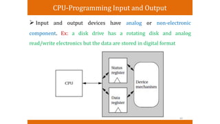
  • 2. CPU-Programming Input and Output  The interface between the CPU and the device’s internals is a set of registers.  Data registers hold values that are treated as data by the device, such as the data read or written by a disk.  Status registers provide information about the device’s operation, such as whether Read only registers. the current transaction has completed. 41
  • 3. Application Example-8251 UART  used for serial communications  UART is programmable for a variety of transmission and reception parameters  Start bit (a 0) allows the receiver to recognize the start of a new character Stop bit (a 1) indicates the end of transmission of data 42
  • 4. Application Example-8251 UART  Baud rate= No of bits transmitted or received/sec  The parameters for the serial communications are,  the baud rate  the number of bits per character (5 through 8)  whether parity is to be included and whether it is even or odd  the length of a stop bit (1, 1.5 or 2 bits)  UART includes one 8-bit register that buffers characters between the UART and the CPU bus 43
  • 5. Application Example-8251 UART  Transmitter Ready output- indicates that the transmitter is ready to send  Transmitter Empty signal goes high when the UART has no characters to send  Receiver Ready pin goes high when the UART has a character ready to be read by the CPU 44
  • 6. Input and Output Primitives  Microprocessors can provide programming support for input and output in two ways: I/O instructions (in and out instructions in Intel x86- These instructions provide a separate address space for I/O devices-Ported I/O) and memory-mapped I/O (provides addresses for the registers in each I/O device)  Programs use the CPU’s normal read and write instructions to communicate with the devices 45
  • 7. Input and Output Primitives 46
  • 8. Memory-mapped I/O in Assembly 47
  • 9. Memory-mapped I/O in C  Traditional names for functions that read and write arbitrary memory locations are peek and poke  To read a device register we can write, 48
  • 10. Memory-mapped I/O in C To write to the status register,  These functions can, of course, be used to read memory locations, not just devices and write arbitrary 49
  • 11. Busy-Wait I/O  I/O devices are much slower than the CPU and may require many cycles to complete an operation.  CPU must wait for one operation to complete before starting the next one. CPU does this by checking device. the status registers of an I/O  Asking an I/O device whether it is finished by reading its status register is often called polling. 50
  • 12. Busy-Wait I/O Programming  To write a sequence of characters to an output device. Device has two registers: one for the character to be written and a status register.  The status register value is 1 when the device is busy writing and 0 when the transaction has completed. 51
  • 14. Interrupts  Busy-wait I/O is extremely inefficient- the CPU does nothing but test the device status while the I/O transaction is in progress. In many cases, the CPU could do useful work in parallel with the transaction, such as, I/O  computation, as in determining the next output to send to device or processing the last input received the  control of other I/O devices  Interrupt mechanism allows devices to signal the CPU and to force execution of a particular piece of code 53
  • 15. Interrupts  When an interrupt occurs, the program counters value is changed to point to an interrupt handler routine (also commonly known as a device driver- that takes care of the device like writing the next data, reading data and so on).  The interrupt mechanism of interruption so that the CPU interrupted. course saves the value of the PC at the can return to the program that was  Interrupts allow the flow of control in the CPU to change easily between different contexts, such as a foreground computation and multiple I/O devices. 54
  • 17. Interrupt Mechanism  Priority based interrupt service- Ex: a program that talks to both a high-speed disk drive and a low-speed keyboard should be designed to finish a disk transaction before handling a keyboard interrupt.  The program that runs when no interrupt is being handled is often called the foreground program. 56
  • 18. Interrupt Mechanism-Example Copying characters from input to output devices with basic interrupts 57
  • 19. Interrupt Mechanism-Example Copying characters from input to output devices with basic interrupts 58
  • 20. Interrupt Mechanism-I/O Buffers Copying characters from input program to output devices with writes interrupts and buffers- independently The performs reads and  Queue is empty  Add characters to the tail when an input is received and take characters from the head when we are ready for output  When the first character is read, the tail is incremented after the character is added to the queue, leaving the buffer and pointers 59
  • 21. Interrupt Mechanism-I/O Buffers  When the buffer is full, we leave one character in the buffer unused.  When the output goes past the end of io_buf, 60
  • 26. Interrupt Mechanism-I/O Buffers-UML Sequence Diagram 65
  • 27. Interrupt Mechanism-I/O Buffers-UML Sequence Diagram  The CPU implements interrupts by checking the interrupt request line at the beginning of execution of every instruction. If an interrupt request has been asserted, the CPU does not fetch the instruction pointed to by the PC.  Instead the CPU sets the PC to a predefined location, which is the beginning of the interrupt handling routine. 66
  • 28. Interrupt Priorities and Vectors  Interrupt priorities allow the CPU to recognize some interrupts as more important than others (Ex: L1-High priority)  Interrupt vectors handler allow the interrupting device to specify its 67
  • 29. Interrupt Priorities and Vectors  Priority mechanism must ensure that a lower priority interrupt does not occur when a higher-priority interrupt is being handled. The decision process is known as masking.  When an interrupt is acknowledged, the CPU stores in an internal register the priority level of that interrupt.  When a subsequent interrupt is received, its priority is checked against the priority register; the new request is acknowledged only if it has higher priority than the currently pending interrupt.  The highest priority interrupt is normally called the non-maskable interrupt (NMI) (Ex: caused by power failures) 68
  • 30. Interrupt Priorities and Vectors  Interrupts with same priority can be serviced by polling mechanism 69
  • 31. Interrupt Vectors  Vector number is stored in device, not the CPU There is no fixed relationship between vector numbers and interrupt handlers. 70
  • 32. Example: I/O with Prioritized Interrupts A- Highest C- Lowest 71
  • 33. Interrupt overhead  Once a device requests an interrupt, some steps are performed by the CPU, some by the device, and others by software.  CPU: Checks for pending interrupts at the beginning of an instruction. It answers the highest priority interrupt, which has a higher priority than that given in the interrupt priority register.  Device: Receives the acknowledgement from CPU and sends the CPU its interrupt vector.  CPU: Looks up the device handler address in the interrupt vector table using the vector as an index. Current value of the PC, internal CPU state and general purpose registers are saved. 72
  • 34. Interrupt overhead  Software: The device driver may save additional CPU state. It then performs the required operations on the device. It then restores any saved state and executes the interrupt return instruction.  CPU: The interrupt return instruction restores the PC and other automatically interrupted. saved states to return execution to the code that was 73
  • 35. Interrupt overhead  Execution time required for the code that devices- Execution time overhead talks directly to the Interrupt causes a change in the program counter, it incurs a branch penalty. In addition, if the interrupt automatically stores CPU registers, that action requires extra cycles, even if the state is not modified by the interrupt handler.  The interrupt requires extra cycles to acknowledge the interrupt and obtain the vector from the device.  Interrupt handler will save and restore CPU registers that were not automatically saved by the interrupt. 74
  • 36. Interrupt overhead  The interrupt return instruction incurs a branch penalty as well as the time required to restore the automatically saved state. 75
  • 37. Interrupts in ARM  ARM7 supports two types of interrupts: fast interrupt requests (FIQs) and interrupt requests (IRQs).  An FIQ takes priority over an IRQ.  The interrupt table is always kept in the bottom memory addresses, starting at location 0.  The entries in the appropriate handler. table typically contain subroutine calls to the 76
  • 38. Interrupts in ARM ARM7 performs the following steps when responding to an interrupt.  saves the appropriate value of the PC to be used to return.  copies the CPSR into a saved program status register (SPSR).  forces bits in the CPSR to note the interrupt, and  forces the PC to the appropriate interrupt vector. When leaving the interrupt handler, the handler should:  restore the proper PC value.  restore the CPSR from the SPSR, and  clear interrupt disable flags. 77
  • 39. Interrupts in ARM The worst case latency to components: respond to an interrupt includes the  two cycles to synchronize the external request.  up to 20 cycles to complete the current instruction.  three cycles for data abort, and  two cycles to enter the interrupt handling state. This adds up to 27 clock cycles. The best case latency is four clock cycle. 78
  • 40. Supervisor mode  Complex systems are often implemented as several programs that communicate with each other. These programs may run under the command of an operating system.  It may be desirable to provide hardware checks to ensure that the programs do not interfere with each other- Additional level of safety.  Normal programs run in user mode.  The supervisor mode has privileges that user modes do not. Control of the memory management unit (MMU) is typically reserved for supervisor mode to avoid inadvertent changes in the memory management registers. 79
  • 41. Supervisor mode in ARM  The ARM instruction that puts the CPU in supervisor mode is called SWI. SWI CODE_1  SWI causes the CPU to go into supervisor mode and sets the PC to 0x08.  The argument to SWI is a 24-bit immediate value that is passed on to the supervisor various services from mode code; it allows the program to request the supervisor mode. 80
  • 42. Supervisor mode in ARM  In supervisor mode, the bottom 5 bits of the CPSR are all set to 1. 2 4 8 7 6 5 4 31 30 29 28 27 I I 0 I J Reserved Field I I IStatus Extention Field Control Field Flag Field 81 Mode bits M[4:0} OblOOOO User Oblllll System OblOOOl AQ Ob10010 IRQ Ob10011 SVC(Supervisor) Ob10111 Abort Ob11011 Undefined Control bits I 1: disables IRQ F 1: disables AQ T 1: Thumb,0: ARM Flag Field N Negative result from ALU z Zero result from ALU c ALU operation caused Carry v ALU operation overflowed Q ALU operation saturated J Java Byte Code Execution
  • 43. Supervisor mode in ARM  The old value of the CPSR just before the SWI is stored in a register called the saved program status register (SPSR). Several SPSRs for different modes, the supervisor SPSR is referred to as SPSR_svc  To return from the supervisor mode, the supervisor restores the PC from register r14 and restores the CPSR from the SPSR_svc. 82
  • 44.
  • 45.
  • 46.
  • 47. Exceptions  An exception is an internally detected zero. error. Ex: division by  The CPU can more efficiently check the divisors value during execution. Since the time at which a zero divisor will be found is not known in advance, this event is similar to an interrupt except that it is generated inside the CPU. The exception mechanism provides a way for the program to react to such unexpected events.  Exceptions are similar to interrupts, however exceptions are generated internally. 83
  • 48. Exceptions  Exceptions in general require both prioritization and vectoring.  Exceptions must be prioritized because a single operation may generate more than one exception. Ex: an illegal operand and an illegal memory access.  The priority of exceptions is usually fixed by the CPU architecture.  Vectoring provides a way for the user to specify the handler for the exception condition.  The vector number for an exception is usually predefined by the architecture; it is used to index into a table of exception handlers. 84
  • 49. Traps  A trap also known as a software interrupt, is an instruction that explicitly generates an exception condition.  The most common use of a trap is to enter supervisor mode.  The entry into supervisor mode must be controlled to maintain security.  The ARM provides the SWI interrupt for software interrupts. This instruction causes the CPU to enter supervisor mode. An opcode is embedded in the instruction that can be read by the handler. 85
  • 50. Co-Processors  Co-processors are attached to the CPU and implement some of the instructions. Ex: floating point arithmetic in Intel architecture.  To support co-processor, certain opcodes must be reserved in the instruction set for co-processor operations.  Because it executes instructions, a co-processor must be tightly coupled to the CPU.  When the CPU receives a co-processor instruction, the CPU must activate the co-processor and pass it the relevant instruction.  Co-processor instructions can load and store co-processor registers or can perform internal operations. 86
  • 51. Co-Processors  The CPU can suspend execution to wait for the co-processor superscalar approach instruction to finish; it can also take a more while and continue executing instructions waiting for the co- processor to finish.  A CPU may, of course, receive co-processor instructions even when there is no co-processor attached. Most architectures use illegal instruction traps to handle these situations.  The trap handler can detect the co-processor instruction and execute it in software instructions in software on the main CPU. Emulating co-processor is slower but provides compatibility. 87
  • 52. Co-Processors in ARM  Supports up to 16 co-processors.  Co-processors are able to perform load and store operations on their own registers.  They can also move data between the co-processor registers and main ARM registers.  Ex: Floating point co-processor- It provides eight 80-bit floating point data registers and floating point status registers. 88
  • 53. Memory System Mechanisms  Modern Microprocessor Units (MMU)- do more than just read and write a monolithic memory. Microprocessor clock rates speeds. are increasing rapidly than memory  Modern Microprocessor Units (MMU) perform address translations that provide physical memory. a larger virtual memory space in a small 89
  • 54. Caches  Caches are widely used to speed up memory system performance.  It speeds up average memory access time when properly used. Hit (data available in Cache memory) and Miss (data not available in Cache memory).  A cache is a small, fast memory that holds copies of some of the contents of main memory. Because the cache is fast, it provides higher-speed access for the CPU; but since it is small, not all the requests can be satisfied by the cache, forcing the system to wait for the slower main memory. 90
  • 55. Caches  Caching makes sense when the CPU is using only a relatively small set of memory locations at any one time; the set of active locations is often called the working set.  Ex: Data read from memory 91
  • 56. Caches in the Memory System  Classification of cache miss A Compulsory Miss ( Cold miss) occurs the first time a location is used. A Capacity Miss is caused by a too-large working set, and A Conflict Miss cache. happens when two locations map to the same location in the 92
  • 57. Memory System Performance where h – hit rate (probability that a given memory the cache) location is in 1- h is the miss rate (probability that location is not in the cache) tav is the average memory access rate tcache tmain is the access time of the cache is the main memory access time 93
  • 58. Memory System Performance  Best case memory access time (ignoring cache controller overhead) is tcache. Few nano seconds.  Worst case access time is tmain. 50-60 ns. 94
  • 59. Multi-level Cache: Two – level cache system  L1 cache- first level (closest to the CPU).  L2 cache- second level cache (feeds the first level cache): much larger but is also slower. 95
  • 60. Two – level cache system where L1 – first-level cache L2 – second-level cache h1 – first-level hit rate h2 is the rate at which access the first- level cache hit the second level cache but not tav is the average memory access rate tmain is the main memory access time 96
  • 61. Data replacement system in cache  As the program working set changes, we expect locations to be removed from the cache to make way for new locations.  One possible replacement policy is least recently used (LRU), that is, throw out the block that has been used farthest in the past. Add relatively small amount of hardware to the cache to keep track of the time since last access of each block.  Another policy is random hardware to implement. replacement, which requires even less 97
  • 62. Direct - Mapped Cache  The cache consists of cache blocks, each of which includes a tag to show which memory location is represented by this block, a data field holding the contents of that memory, and a valid. valid tag to show whether the contents of this cache block are 98
  • 63. Direct - Mapped Cache  An address is divided into three sections.  Index – used to select which cache block to check  Address tag is compared with cache tag selected by the index. If it matches, that block includes the desired memory location.  If the length of the data field is longer than the minimum addressable unit, then the lowest bits of the address are used as an offset to select the value from the data field. required  If the access is a hit, the data value is read from the cache. 99
  • 64.
  • 65.
  • 66. Direct - Mapped Cache Writing the data in cache needs updation of main memory too. Write – Through scheme (every write changes both the cache and the corresponding main memory location- usually through the write buffer). This method ensures that the cache and main memory are consistent, but may generate some additional main memory traffic. n Write – Back Policy (We write only when we remove written a location from the cache, we eliminate the writes it is removed from cache) when a location is several times before 100
  • 67. Direct - Mapped Cache  Advantage: Is fast and relatively low cost.  Disadvantage: If two popular locations in a program happen to map onto cache. the same block, we will not gain the full benefits of the 101
  • 68. Set - Associative Cache  A set-associative cache is characterized by the number of banks or ways it uses, giving an n-way set associative cache. 102
  • 69. Set - Associative Cache  A set is formed by all the blocks (one for each bank) that shares the same index. Each set is implemented with a direct-mapped cache.  A cache request is broadcast to all the banks simultaneously.  If any of the sets has the location, the cache reports a hit. 103
  • 70. Set - Associative Cache  Therefore, we can simultaneously cache several locations that happen to map onto the same cache block.  It incurs a little extra overhead and is slightly slower than the direct mapped cache, but has higher hit rates. 104
  • 71. Direct mapped vs Set - Associative Cache Example: 2 bits of the address as tag.  Direct mapped cache with four blocks  two way set associative cache with four sets  We use Least recently used (LRU) replacement to make it easy to compare the two caches. 105
  • 72. Direct mapped vs. Set - Associative Cache 106
  • 73. Direct mapped vs. Set - Associative Cache Direct mapping- 001, 010, 011, 100, 101 and 111 107
  • 74. Direct mapped vs. Set - Associative Cache Set-Associative mapping- 001, 010, 011, 100, 101 and 111 Four set-two way associative mapping 108
  • 75. Caches in ARM  A cache that holds both instructions and data is called a unified cache.  ARM 600 includes a 4 KB, 64 way unified instruction/data cache.  The Strong ARM uses a 16 KB, 32-way instruction cache with a 32- byte data block cache and a 16 KB, 32 way data cache with a 32-byte block; the uses a write-back strategy. 109
  • 76. Memory Management Units and Address Translation  A memory management unit (MMU) translates addresses between the CPU and physical memory- Memory mapping (addresses are mapped from a logical space into a physical space)  When memory became cheap enough that physical memory could be larger than the address space defined by the instruction, MMUs allowed software to manage multiple programs in a single physical memory, each with its own address space- Virtual addressing.  Use physical DRAM (Main memory) as a cache for the secondary storage (Flash, disk) 110
  • 77. Memory Management Units and Address Translation  MMU accepts logical addresses from the CPU. Logical addresses refer to the program’s abstract address space but do not correspond to actual RAM locations.  The MMU translates them from tables to physical addresses that do correspond to RAM. 111
  • 78. Memory Management Units and Address Translation  By changing the MMU’s tables. you can change the physical location at which the program resides without modifying the program’s code or data.  In a virtual memory system, the addresses are actually resident in MMU keeps track of which logical main memory; those that do not reside in main memory are kept on the secondary storage device.  When the CPU requests an address that is not in main memory, the MMU generates an exception called a page fault. The handler for this exception executes code that reads the requested location from the secondary storage device into main memory. 112
  • 79. Memory Management Units and Address Translation  The program that generated the page fault is restarted by the handler only after, The required memory has been read back into main memory, and The MMU tables have been updated to reflect the changes.  The displaced memory is copied into secondary storage before the requested location is read in. As with caches, LRU is a good replacement policy. 113
  • 80. Address Translation  Two styles of Address Translation are, Segmented Paged  Two can also be combined to form a segmented, paged addressing scheme.  Segmenting is designed to support a large, arbitrarily sized region of memory, while pages describe small, equally sized regions. 114
  • 82. Address Translation-Segments and Pages  A segment is usually described by its start address and size, allowing different segments to be of different sizes.  Pages are of uniform size, which simplifies the hardware required for address translation.  A segmented, paged scheme is created by dividing each segment into pages and using two steps for address translation.  Paging introduces the possibility of fragmentation as program pages are scattered around physical memory. 116
  • 83. Address Translation for a segment 117
  • 84. Address Translation for a segment 118
  • 85. Address Translation for a segment 119
  • 86. Address Translation for a segment  The MMU would maintain a segment register that describes the the currently active segment. This register would point to the base current segment. of  The address extracted from an instruction (or from any source for addresses, such as a register) would be used as the for the address. other offset The physical address is formed by adding the segment base offset. to the  The segment register may also include the segment size and compare the offset to the allowed size. 120
  • 88. Address Translation for a page  The logical address is divided into two sections, including a page number and an offset. The page number is used as an index into a page table, which stores the physical address for the start of each page. Since all pages have the same size, the MMU simply needs to concatenate the top bits of the page starting address with the bits from the page offset to form the physical address. bottom Pages are small, typically between 512 bytes and 4 KB. The page table (kept in main memory- requires an memory is large for an architecture with a large address space. access) 122
  • 89. Page table organization  Page table may be organized in several ways,  Flat table (The table is indexed by the page number and each entry holds the page descriptor)  Tree structured ( The root entry of the tree holds pointers to pointer tables at the next level of the tree; each pointer table is indexed by a part of the page number. We eventually (after three levels, in this case) arrive at a descriptor table that includes the page descriptor we are interested in.)  A tree-structured page table incurs some overhead for the pointers, but it allows us to build a partially populated tree. If some part of the address space part of the tree that covers is it. not used, we do not need to build the 123
  • 91. Address Translation The efficiency of paged address translation may be increased by caching page translation information.  A cache for address translation is known as a translation lookaside buffer (TLB).  The MMU reads the TLB to check whether a page number is currently in the TLB cache reading from memory. and, if so, uses that value rather than 125
  • 94. Address Translation-TLB  When a Virtual Address is accessed, and then looked up, the TLB Cache is checked first to see if the Virtual-Physical Address mapping is present and if so then a TLB Hit occurs.  On the other hand, if the address isn't present, then a TLB Miss occurs and the MMU is forced to execute a Page Walk which is the process of looking through the Page Tables.  Once, the Page Walk has completed and the physical address is found, then this information is loaded into the TLB Cache.  If Page Walk is unsuccessful, then a Page Fault is raised, and the Virtual to Physical Address Mapping is created in the Page Table. 128
  • 95. Address Translation Criteria required for segmenting and paging for virtual memory At minimum, a present bit is necessary to show whether the logical segment or page is currently in physical memory. A dirty bit shows whether the page/segment has been written to. This bit is maintained by the MMU, since it knows about every write performed by the CPU. Permission bits are often used. Some pages/ segments may be readable but not writable. If the CPU support modes, pages/ segments may be accessible by the supervisor but not in user mode.  A data or instruction cache may operate either on logical or physical addresses, depending on where it is positioned relative to the MMU. 129
  • 96. MMU in ARM  A MMU is an optional part of the ARM architecture. The ARM MMU supports both virtual address translation and memory protection; the architecture requires that the MMU be implemented when cache or write buffers are implemented. The ARM MMU supports the following address translation: Section (1 MB block of memory) types of memory regions for Large page (64 KB) Small Page (4 KB) 130
  • 97. ARM MMU Address translation An address is marked as section mapped or page mapped.  A two-level scheme is used to translate addresses.  The first-level table, which is pointed to by the Translation Table Base register, holds descriptors for section translation and pointers to the second-level tables.  The second-level tables describe the translation of both large and small pages. The first- and second-level pages also contain access control bits for virtual memory and protection. 131
  • 98. ARM Two- stage address translation - Virtual address Second-level Index Offset Second-level table 132 ... First-level Index First-level descriptor I Concatenate First-level table Second-level descriptor Concatenate Physical address TranslaUon Table Base resister
  • 99. CPU Performance-Pipelining  Modern CPUs are designed as pipelined machines in which several instructions are executed in parallel.  Pipelining greatly increases the efficiency of the CPU.  Branch and go to statements affect the performance of pipelining in CPU. 133
  • 100. ARM 7 Pipelining  Three – stage pipelining. Fetch – instruction fetched from memory. Decode – instruction’s opcode and operands determine the function to perform. are decoded to Execute – the decoded instruction is executed. Each stage requires one clock cycle per instruction Latency- 3 clock cycles required for single instruction without pipelining execution Pipelining has a throughput of one instruction per cycle. 134
  • 101. Pipelined execution of ARM Instructions Extended execution is when an instruction is too complex to complete the execution phase in a single cycle. Example: Multiple load instruction (ldmia r0,[r2,r3]) 135
  • 102. Pipelined execution of multicycle ARM Instruction Data stall in the execution of a sequence of instructions.  In multiphase execution, the decode stage is also occupied, since it must continue to remember the decoded instruction. 136
  • 103. Pipelined execution of a branch in ARM  Branches also introduce control stall delays into the pipeline, commonly referred to as the branch penalty.  The CPU uses the two cycles between starting to fetch the branch target and starting to execute that instruction. 137
  • 104. Caching Although caches are invisible in the programming model, they have a profound effect on performance.  The extra time required to access a memory location not in the cache is often called the cache miss penalty. Data may not be available in cache due to several reasons: At a compulsory miss, the location has not been referenced before. At a conflict miss, two particular memory locations are fighting for the same cache line. At a capacity miss, the program’s working set is simply too large for the cache. 138
  • 105. Caching  When we have several programs running concurrently on the CPU, we can have very dramatic changes in the cache contents. 139
  • 106. CPU Power Consumption  Power consumption is as important as execution time. Power- energy consumption per unit time.  Heat generation depends on power consumption.  Battery life depends on energy consumption.  Today, virtually all digital systems are built with complementary metal oxide semiconductor (CMOS) circuitry.  The basic sources of CMOS power consumption are: Voltage Drops (dynamic power consumption ∝ square of power supply voltage (V2)). Reducing the power supply voltage to the lowest that provide the required performance and also by using additional parallel hardware. 140
  • 107. CPU Power Consumption Toggling- A CMOS circuit uses most of its power when it is changing its output value. By reducing the speed at which the circuit operates, we can reduce its power consumption. Eliminating unnecessary glitches at the circuit input and output eliminates unnecessary power consumption. Leakage- Even when a CMOS circuit is not active, some charge leaks out of the circuit nodes through the substrate. The only way to eliminate leakage current is to remove the power supply but it for rebooting the system. usually takes a significant amount of time 141
  • 108. Power Saving Strategies used in CMOS CPUs CPUs can be used at reduced voltage levels. by reducing supply causing power consumption reduction. power CPU can be operated at a lower clock frequency to reduce consumption. power CPU may internally disable certain function function, units that are not required for the currently executing thereby reducing energy consumption. Some CPUs allow parts of the CPU to be totally disconnected from the power supply to eliminate leakage currents. 142
  • 109. Power management features provided by CPUs Static power management mechanism-is invoked by the user but does not otherwise depend on CPU activities. Example: power down mode intended to save energy. Instruction based mode activation. Power-down modes typically end upon receipt of an interrupt or other events. Dynamic power management mechanism takes actions to control power based upon the dynamic activity in the CPU when the instructions being executed do not need them. 143
  • 110. Power saving modes of Strong ARM SA-1100 Run mode - highest power consumption. Idle Mode – saves power by saving the CPU Clock. Sleep mode – shuts off most of the chip’s activity three orders of magnitude of power consumption. and saves about Time taken second. to reenter run mode from sleep is over a tenth of a 144
  • 111. Power saving modes of Strong ARM SA-1100 145
  • 112. Design Example: Data Compressor Data compressor takes in data with a constant number of bits per data data element and puts out a compressed data stream in which the is encoded in variable length symbols. 146
  • 113. Requirements and Algorithm Huffman coding technique is used for data compression.  The data compressor takes in a sequence of input symbols and then produces a stream of output symbols.  Assume input symbols of one byte in length.  The output symbols are variable length, so we have to choose a format in which to deliver the output data. (code, length).  Bit by bit delivery is also too slow.  Data compressor is going to pack the coded symbols into an array. 147
  • 114. Huffman coding for text compression Text compression algorithms aim at statistical reductions in the volume of data.  Huffman coding makes use of information on the frequency of characters to assign variable length codes to characters.  Shorter bit sequences are used to identify more frequent characters, then the length of the total sequence will be reduced.  To decode the incoming bit string, the code characters must have unique prefixes. 148
  • 115. Huffman coding for text compression Example: Assume that these characters have the following probabilities P of appearance in a message.  Bottom up approach 149
  • 116. Huffman coding for text compression 150
  • 117. Huffman coding for text compression Reading the codes off the tree from the root to the leaves, we obtain the following coding of the characters. 151
  • 119. Data compressor- Specification For a fully functional system (dynamic),  We have to be able to provide the compressor with a new symbol table.  We should be able to flush the symbol buffer to cause the system to release all pending symbols that have been partially packed. We may want to do this when we change the symbol table or in the middle of an encoding session to keep the transmitter busy. 153
  • 121. Data compressor- Specification The class’s buffer and current-bit behaviors keep track of the encoding. of the state  The table attribute provides the current symbol table.  The class has three methods as follows:  Encode performs the basic encoding function. It takes in a 1-byte input symbol and returns two values: a boolean showing whether it is returning a full buffer.  New symbol-table installs a new symbol table into the object and throws away the current contents of the internal buffer. 155
  • 122. Data compressor- Specification  Flush returns the current state of the buffer, including the number of valid bits in the buffer. 156
  • 125. Data compressor- Specification  The data buffer will be used to hold both packed and unpacked symbols (such as in symbol table). It defines the buffer itself and the length of the buffer.  The insert function packs a new symbol into the upper bits of the buffer; it also puts the remaining bits in buffer is overflowed. a new buffer if the current  The symbol-table class indexes the symbol. encoded version of each  The load function is used to create a new symbol table. 159