Electronics I and Lab
DC Analysis of Transistor and DC Load Line
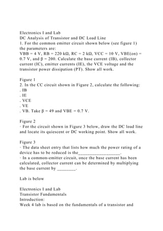
1. For the common emitter circuit shown below (see figure 1) the parameters are:
VBB = 4 V, RB = 220 kΩ, RC = 2 kΩ, VCC = 10 V, VBE(on) = 0.7 V, and β = 200. Calculate the base current (IB), collector current (IC), emitter currents (IE), the VCE voltage and the transistor power dissipation (PT). Show all work.
Figure 1
2. In the CC circuit shown in Figure 2, calculate the following:
. IB
. IE
. VCE
. VE
. VB. Take β = 49 and VBE = 0.7 V.
Figure 2
· For the circuit shown in Figure 3 below, draw the DC load line and locate its quiescent or DC working point. Show all work.
Figure 3
· The data sheet entry that lists how much the power rating of a device has to be reduced is the__________________.
· In a common-emitter circuit, once the base current has been calculated, collector current can be determined by multiplying the base current by ________.
Lab is below
Electronics I and Lab
Transistor Fundamentals
Introduction:
Week 4 lab is based on the fundamentals of a transistor and analysis of an analog circuit.
Please review the following videos before getting started with this lab:
1. Watch the video: “Video 3: Fundamentals of breadboard”
2. Watch the video: “Video 4: Basic electrical components”
3. Watch the video: “Video 5: Simple resistive circuit with NI myDAQ”
Materials and Equipment:
Materials:
· Hardware Parts (In the Toolbox):
. An NPN transistor: 2N3904
. Two resistors: 10 kΩ and 3.6 kΩ
. Jumper wires
Equipment:
· Hardware Equipment:
. Breadboard
. NI myDAQ Instrument device
. Screw Driver
. Screw Terminal connector
. USB Cable
. Multimeter probes
. Oscilloscope, Multimeter and Function generator from NI ELVISmx Intrument Launcher
Procedure:
*** This lab has to be implemented only in hardware (using NI myDAQ) ***
1. Analyze the circuit in the Figure 1 below to calculate the following values: VE, IE, VRC, VC, VCE. Make sure to include 20% tolerance for each resistor in the calculations.
2. Construct the circuit shown in Figure 1 below on the breadboard using the transistor and two resistors (RCand RE).
3. Using the jumper wires, screw driver and screw terminal connector, connect the board to NI MyDAQ Instrument Device.
4. Use channel +15V pin out on the NI myDAQ Instrument Device to provide the supply voltage (VCC) and channel AO0 to provide the base voltage (VBB). Make sure that this voltage is peak-to-peak. Use channel AI0 to measure the required voltages using the oscilloscope.
Figure 1
5. Using the function generator from NI ELVISmx Instrument Launcher, provide the input voltage VBB to the circuit.
6. Use the oscilloscope to measure the voltages: VE, VRC, VC, VCE.
7. Now, using multimeter with the probes, measure the required voltages: VE, VRC, VC, VCEand currents: IC and IE.
8. Tabulate the values obtained in step 1 and 7.
Calculated
Measured
VE
IE
VRC
VC
VCE
Review questions:
1. Compare the calculated and measured values in the table and analyze the pe ...
Electronics I and LabDC Analysis of Transistor and DC Load Line.docx
1. Electronics I and Lab
DC Analysis of Transistor and DC Load Line
1. For the common emitter circuit shown below (see figure 1)
the parameters are:
VBB = 4 V, RB = 220 kΩ, RC = 2 kΩ, VCC = 10 V, VBE(on) =
0.7 V, and β = 200. Calculate the base current (IB), collector
current (IC), emitter currents (IE), the VCE voltage and the
transistor power dissipation (PT). Show all work.
Figure 1
2. In the CC circuit shown in Figure 2, calculate the following:
. IB
. IE
. VCE
. VE
. VB. Take β = 49 and VBE = 0.7 V.
Figure 2
· For the circuit shown in Figure 3 below, draw the DC load line
and locate its quiescent or DC working point. Show all work.
Figure 3
· The data sheet entry that lists how much the power rating of a
device has to be reduced is the__________________.
· In a common-emitter circuit, once the base current has been
calculated, collector current can be determined by multiplying
the base current by ________.
Lab is below
Electronics I and Lab
Transistor Fundamentals
Introduction:
Week 4 lab is based on the fundamentals of a transistor and
2. analysis of an analog circuit.
Please review the following videos before getting started with
this lab:
1. Watch the video: “Video 3: Fundamentals of breadboard”
2. Watch the video: “Video 4: Basic electrical components”
3. Watch the video: “Video 5: Simple resistive circuit with NI
myDAQ”
Materials and Equipment:
Materials:
· Hardware Parts (In the Toolbox):
. An NPN transistor: 2N3904
. Two resistors: 10 kΩ and 3.6 kΩ
. Jumper wires
Equipment:
· Hardware Equipment:
. Breadboard
. NI myDAQ Instrument device
. Screw Driver
. Screw Terminal connector
. USB Cable
. Multimeter probes
. Oscilloscope, Multimeter and Function generator from NI
ELVISmx Intrument Launcher
Procedure:
*** This lab has to be implemented only in hardware (using NI
myDAQ) ***
1. Analyze the circuit in the Figure 1 below to calculate the
following values: VE, IE, VRC, VC, VCE. Make sure to include
20% tolerance for each resistor in the calculations.
2. Construct the circuit shown in Figure 1 below on the
breadboard using the transistor and two resistors (RCand RE).
3. Using the jumper wires, screw driver and screw terminal
connector, connect the board to NI MyDAQ Instrument Device.
4. Use channel +15V pin out on the NI myDAQ Instrument
Device to provide the supply voltage (VCC) and channel AO0 to
provide the base voltage (VBB). Make sure that this voltage is
3. peak-to-peak. Use channel AI0 to measure the required voltages
using the oscilloscope.
Figure 1
5. Using the function generator from NI ELVISmx Instrument
Launcher, provide the input voltage VBB to the circuit.
6. Use the oscilloscope to measure the voltages: VE, VRC, VC,
VCE.
7. Now, using multimeter with the probes, measure the required
voltages: VE, VRC, VC, VCEand currents: IC and IE.
8. Tabulate the values obtained in step 1 and 7.
Calculated
Measured
VE
IE
VRC
VC
VCE
Review questions:
1. Compare the calculated and measured values in the table and
analyze the performance of the transistor.
2. Discuss whether the values are the same or different. If they
are different, provide the reasoning and explain how to reduce
this difference between calculated and measured values.
4. 3. Explain what happens when the transistor changes to a PNP
transistor. How does the change in the transistor effect the
current and voltage in the circuit?
Deliverables:
1. Analysis of the circuit and calculations of voltages: VE,
VRC, VC, VCE and currents: IC and IE.
2. Place your student ID card on the breadboard and take a
picture of the circuit board and pin out on the NI myDAQ
Instrument Device.
3. Take screenshots of the measurements obtained from function
generator and Multimeter on the NI ELVISmx Instrument
Launcher on your screen.
Lab Report:
· Use the Lab report template found in the “Tools and
Template” link in the navigation center.
· Include all the deliverables.
· Include all the screenshots of the measurements from
Multisim, circuit design on the breadboard using NI myDAQ
device and measurements from MI ELVISmx Instrument
Launcher.
· Save the document as Lab4YourGID.docx (ex:
Lab4G00000000.docx) and submit in Blackboard.
Grading Rubrics:
Grading Criteria
Points
Analysis of the transistor circuit in Figure 1 using an NPN
transistor
15
Including 20% tolerances in the calculations
10
Construct the circuit in Figure 1 on the breadboard
20
Interfacing the breadboard with the NI myDAQ using
appropriate pins
10
Measurement of the voltages: VE, VRC, VC, VCE using the
5. Oscilloscope and Multimeter probes
10
Measurement of currents: IE and IC using the Multimeter
probes
10
Table and Review Questions
15
Report format (Proper use of template)
10
TOTAL
100
This assignment is Due Tuesday December 27th 2016
Ford Motor Co. is the selected company
Based on the company which is Ford Motor Co. that has been
selected for your client's investment, prepare an analysis of
financing strategies you would propose to pursue your
recommendation. Use 1 to 5 pages.
Include a discussion of the following topics in your financing
strategy analysis for Ford Motor Co.
· Capital structure analysis.
· Various debt and equity instruments.
· Impact on risk, return, earnings per share, price-earnings
ratios, price per share, and company value.
· Valuation of financial assets (stocks and bonds) used to carry
out the deal.
6. · Analysis of current dividend policies: any proposed changes.
· Analysis of merger or divestiture activities.
· Analysis of any leasing activities.