SlideShare a Scribd company logo
1 of 5
Department of Electrical Engineering
Faculty of Engineering & Applied Sciences
Riphah International University, Islamabad, Pakistan
Program: B.Sc. Electrical Engineering Semester: III
Subject EE-241 Basic Electronics Date:
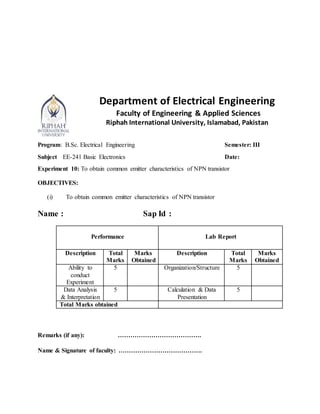
Experiment 10: To obtain common emitter characteristics of NPN transistor
OBJECTIVES:
(i) To obtain common emitter characteristics of NPN transistor
Name : Sap Id :
Performance Lab Report
Description Total
Marks
Marks
Obtained
Description Total
Marks
Marks
Obtained
Ability to
conduct
Experiment
5 Organization/Structure 5
Data Analysis
& Interpretation
5 Calculation & Data
Presentation
5
Total Marks obtained
Remarks (if any): ………………………………….
Name & Signature of faculty: ………………………………….
Introduction Of Theory:-
The transistor is a two junction, three terminal semiconductor device which has three
regionsnamely the emitter region, the base region, and the collector region. There
are two types oftransistors. An npn transistor has an n type emitter, a p type base and an n
type collector while a pnptransistor has a p type emitter, an n type base and a p type collector.
The emitter is heavily doped,base region is thin and lightly doped and collector is moderately
doped and is the largest. The current conduction in transistors takes place due to both charge
carriers- that is electrons and holes and hencethey are named Bipolar Junction Transistors (BJT).
We will obtain input characteristics and output characteristics of common emitter (CE)
configuration. We will connect variable DC power supply at VBB and VCC to obtain
characteristics. Input voltage in CE configuration is base-emitter voltage Vbe and input current
is base current Ib. Output voltage in CE configuration is collector to emitter voltage VCE and
output current is collector current Ic. We will use multi-meter to measure these voltages and
currents for different characteristics. Collector to emitter junction is reverse biased and base to
emitter junction is forward biased. The CE configuration is widely used in amplifier circuits
because it provides voltage gain as well as current gain. In CB configuration current gain is less
than unity. In CC configuration voltage gain is less than unity. Input resistance of CE
configuration is less than CC configuration and more than CB configuration. Output resistance
of CE configuration is more than CC configuration and less than CB configuration.
Circuit setup for input characteristics:
Experiment procedure:
.Connect circuit as shown in the circuit diagram for input characteristics
.Connect variable power supply 0-30V at base circuit and collector circuit.
.Keep Vcc fix at 0V (Or do not connect Vcc)
.Increase VBB from 0V to 20V, note down readings of base current Ib and base to emitter
voltage Vbe in the observation table.
.Repeat above procedure for Vcc = +5V and Vcc = +10V
.Draw input characteristics curve. Plot Vbe on X axis and Ib on Y axis.
Observation table:
Sr. No. Vcc = 0V Vcc = 5V Vcc = 10V
Vbe Ib Vbe Ib Vbe Ib
1 0.52 10 0.5 10 0.5 10
2 0.54 30 0.5 30 0.56 30
3 0.54 50 0.5 50 0.56 50
4 0.54 70 0.52 70 0.56 70
5 0.55 90 0.54 90 0.56 90
6 0.55 110 0.54 110 0.57 110
7 0.56 140 0.56 140 0.57 140
8 0.56 160 0.57 160 0.57 160
9 0.57 180 0.57 180 0.57 180
10 0.57 200 0.57 200 0.57 200
Input Characteristics:
Circuit setup for output characteristics:
Experiment Procedure:
.Connect circuit as shown in the circuit diagram for output characteristics
.Connect variable power supply 0-30V at base circuit and collector circuit.
.Keep base current fix (Initially 0)
.Increase VCC from 0V to 30V, note down readings of collector current Ic and
collector to emitter voltage Vce in the observation table.
.Repeat above procedure for base currents Ib = 5μA, 50 μA, 100 μA. Increase base
current by increasing VBB.
.Draw output characteristics curve. Plot Vce on X axis and Ic on Y axis.
Observation table:
Sr. Ib = 0µA Ib = 5µA Ib = 50µA Ib = 100µA
No. Vce Ic Vce Ic Vce Ic Vce Ic
1 0.008 0 0.02 5 0.5 1.8 1 15.9
2 0.003 0 1.8 780 0.8 5.2 2 30.8
3 5.5 0 4.6 792 0.9 8.4 3 32.6
4 8.5 0 8.4 796 3.4 10 4 36.4
5 11.6 0 11.2 804 5 11.1 5 37.4
6 16.2 0 14.02 806 5.9 11.5 6 39.6
7 19.2 0 16.08 812 10.9 11.8 7 41.1
8 22.1 0 18 816 13 11.85 8 42.8
9 22.2 0 19.6 818 14 12.25 9 43.9
10 22.8 0 20.03 912 15 13.45 10 45.0
Output Characteristics:
Discussion of Results :-
In this lab we have to learnt about the behavior of transistor and also study about
thecommon emitter amplifier and also find the voltages and current with help of DMM
havingdifferent values. After that find the output and input voltages by the given circuit and
make thewaveform with the help of different values.
Conclusion:
This lab is about to common emitter characteristics of NPN transistor.After that observe the
working of common emitter amplifier. And find the input and output voltages and currents.
After that make the waveform ofdifferent values.

More Related Content

What's hot

Lecture trans bias_1
Lecture trans bias_1Lecture trans bias_1
Lecture trans bias_1Napex Terra
 
Lab 8 bipolar junction transistor characterstics
Lab 8  bipolar junction transistor charactersticsLab 8  bipolar junction transistor characterstics
Lab 8 bipolar junction transistor charactersticskehali Haileselassie
 
Hybrid model for Transistor, small signal Analysis
Hybrid model for Transistor, small signal AnalysisHybrid model for Transistor, small signal Analysis
Hybrid model for Transistor, small signal AnalysisAbhishek Choksi
 
Bjt amplifiers
Bjt amplifiersBjt amplifiers
Bjt amplifiersGastarot
 
Mba admssion in india
Mba admssion in indiaMba admssion in india
Mba admssion in indiaEdhole.com
 
Chapter 2: Direct Current (DC) Circuits
Chapter 2: Direct Current (DC) CircuitsChapter 2: Direct Current (DC) Circuits
Chapter 2: Direct Current (DC) CircuitsJeremyLauKarHei
 
Diode voltage multiplier
Diode voltage multiplierDiode voltage multiplier
Diode voltage multiplierUnsa Shakir
 
Electronics 1 : Chapter # 05 : DC Biasing BJT
Electronics 1 : Chapter # 05 : DC Biasing BJTElectronics 1 : Chapter # 05 : DC Biasing BJT
Electronics 1 : Chapter # 05 : DC Biasing BJTSk_Group
 
EE 305 Project_1 The Effective External Defibrillators
EE 305 Project_1 The Effective External Defibrillators EE 305 Project_1 The Effective External Defibrillators
EE 305 Project_1 The Effective External Defibrillators kehali Haileselassie
 
Bipolar junction transistor characterstics biassing and amplification, lab 9
Bipolar junction transistor characterstics biassing and amplification, lab 9Bipolar junction transistor characterstics biassing and amplification, lab 9
Bipolar junction transistor characterstics biassing and amplification, lab 9kehali Haileselassie
 
EST 130, Transistor Biasing and Amplification.
EST 130, Transistor Biasing and Amplification.EST 130, Transistor Biasing and Amplification.
EST 130, Transistor Biasing and Amplification.CKSunith1
 

What's hot (20)

Lecture trans bias_1
Lecture trans bias_1Lecture trans bias_1
Lecture trans bias_1
 
Lab 8 bipolar junction transistor characterstics
Lab 8  bipolar junction transistor charactersticsLab 8  bipolar junction transistor characterstics
Lab 8 bipolar junction transistor characterstics
 
Hybrid model for Transistor, small signal Analysis
Hybrid model for Transistor, small signal AnalysisHybrid model for Transistor, small signal Analysis
Hybrid model for Transistor, small signal Analysis
 
EC6202 ELECTRONIC DEVICES AND CIRCUITS Unit 2
EC6202 ELECTRONIC DEVICES AND CIRCUITS Unit 2EC6202 ELECTRONIC DEVICES AND CIRCUITS Unit 2
EC6202 ELECTRONIC DEVICES AND CIRCUITS Unit 2
 
Cbcs b sc i sem e1 unit 1
Cbcs b sc i sem e1 unit 1Cbcs b sc i sem e1 unit 1
Cbcs b sc i sem e1 unit 1
 
EC6202 ELECTRONIC DEVICES AND CIRCUITS NOTES
EC6202 ELECTRONIC DEVICES AND CIRCUITS NOTESEC6202 ELECTRONIC DEVICES AND CIRCUITS NOTES
EC6202 ELECTRONIC DEVICES AND CIRCUITS NOTES
 
Bjt amplifiers
Bjt amplifiersBjt amplifiers
Bjt amplifiers
 
Mba admssion in india
Mba admssion in indiaMba admssion in india
Mba admssion in india
 
Chapter 2: Direct Current (DC) Circuits
Chapter 2: Direct Current (DC) CircuitsChapter 2: Direct Current (DC) Circuits
Chapter 2: Direct Current (DC) Circuits
 
Diode voltage multiplier
Diode voltage multiplierDiode voltage multiplier
Diode voltage multiplier
 
Bsc 1 cbcs e1 unit 2
Bsc 1 cbcs e1 unit 2Bsc 1 cbcs e1 unit 2
Bsc 1 cbcs e1 unit 2
 
Cbcs e1 unit 3
Cbcs e1 unit 3Cbcs e1 unit 3
Cbcs e1 unit 3
 
Transistor configurations
Transistor configurationsTransistor configurations
Transistor configurations
 
Diodes vi characteries
Diodes vi characteriesDiodes vi characteries
Diodes vi characteries
 
Electronics 1 : Chapter # 05 : DC Biasing BJT
Electronics 1 : Chapter # 05 : DC Biasing BJTElectronics 1 : Chapter # 05 : DC Biasing BJT
Electronics 1 : Chapter # 05 : DC Biasing BJT
 
207137236 ee2207-lm
207137236 ee2207-lm207137236 ee2207-lm
207137236 ee2207-lm
 
Linear Integrated Circuit
Linear Integrated Circuit Linear Integrated Circuit
Linear Integrated Circuit
 
EE 305 Project_1 The Effective External Defibrillators
EE 305 Project_1 The Effective External Defibrillators EE 305 Project_1 The Effective External Defibrillators
EE 305 Project_1 The Effective External Defibrillators
 
Bipolar junction transistor characterstics biassing and amplification, lab 9
Bipolar junction transistor characterstics biassing and amplification, lab 9Bipolar junction transistor characterstics biassing and amplification, lab 9
Bipolar junction transistor characterstics biassing and amplification, lab 9
 
EST 130, Transistor Biasing and Amplification.
EST 130, Transistor Biasing and Amplification.EST 130, Transistor Biasing and Amplification.
EST 130, Transistor Biasing and Amplification.
 

Similar to Basic lab 10

My_lec_Bipolar_Junction_Transistor_text_book.pdf
My_lec_Bipolar_Junction_Transistor_text_book.pdfMy_lec_Bipolar_Junction_Transistor_text_book.pdf
My_lec_Bipolar_Junction_Transistor_text_book.pdfElorme
 
Bipolar junction transistor characterstics biassing and amplification, lab 9
Bipolar junction transistor characterstics biassing and amplification, lab 9Bipolar junction transistor characterstics biassing and amplification, lab 9
Bipolar junction transistor characterstics biassing and amplification, lab 9kehali Haileselassie
 
Electronics and modern physics presentation
Electronics and modern physics presentationElectronics and modern physics presentation
Electronics and modern physics presentationNoorulainRazzaq
 
(Latest) topic 4 bipolar_junction_transistors
(Latest) topic 4 bipolar_junction_transistors(Latest) topic 4 bipolar_junction_transistors
(Latest) topic 4 bipolar_junction_transistorsGabriel O'Brien
 
Lecture 06 transistorremodel
Lecture 06 transistorremodelLecture 06 transistorremodel
Lecture 06 transistorremodelIsmael Cayo Apaza
 
Intro electronics laboratory
Intro electronics laboratoryIntro electronics laboratory
Intro electronics laboratoryThinh Pham Quoc
 
Multisim_simulation_project_3_^0_4[1]-2.pptx
Multisim_simulation_project_3_^0_4[1]-2.pptxMultisim_simulation_project_3_^0_4[1]-2.pptx
Multisim_simulation_project_3_^0_4[1]-2.pptxwencove9
 
BJT Biasing for B.Tech Ist Year Engineering
BJT Biasing for B.Tech Ist Year EngineeringBJT Biasing for B.Tech Ist Year Engineering
BJT Biasing for B.Tech Ist Year EngineeringRaghav Bansal
 
BJT BIASING-SOWMIYA.pdf
BJT BIASING-SOWMIYA.pdfBJT BIASING-SOWMIYA.pdf
BJT BIASING-SOWMIYA.pdfGunaG14
 
Chapter-6 DC biasing-1.ppt
Chapter-6 DC biasing-1.pptChapter-6 DC biasing-1.ppt
Chapter-6 DC biasing-1.pptJeelBhanderi4
 
Single stage bjt amplifier. experiment 6
Single stage bjt amplifier. experiment 6Single stage bjt amplifier. experiment 6
Single stage bjt amplifier. experiment 6Karimi LordRamza
 
Transistor Configuration
Transistor Configuration Transistor Configuration
Transistor Configuration Smit Shah
 

Similar to Basic lab 10 (20)

My_lec_Bipolar_Junction_Transistor_text_book.pdf
My_lec_Bipolar_Junction_Transistor_text_book.pdfMy_lec_Bipolar_Junction_Transistor_text_book.pdf
My_lec_Bipolar_Junction_Transistor_text_book.pdf
 
Transistor 1 lecture
Transistor 1 lectureTransistor 1 lecture
Transistor 1 lecture
 
Transistors.ppt
Transistors.pptTransistors.ppt
Transistors.ppt
 
Bipolar junction transistor characterstics biassing and amplification, lab 9
Bipolar junction transistor characterstics biassing and amplification, lab 9Bipolar junction transistor characterstics biassing and amplification, lab 9
Bipolar junction transistor characterstics biassing and amplification, lab 9
 
Electronics and modern physics presentation
Electronics and modern physics presentationElectronics and modern physics presentation
Electronics and modern physics presentation
 
(Latest) topic 4 bipolar_junction_transistors
(Latest) topic 4 bipolar_junction_transistors(Latest) topic 4 bipolar_junction_transistors
(Latest) topic 4 bipolar_junction_transistors
 
Lecture 06 transistorremodel
Lecture 06 transistorremodelLecture 06 transistorremodel
Lecture 06 transistorremodel
 
Intro electronics laboratory
Intro electronics laboratoryIntro electronics laboratory
Intro electronics laboratory
 
Multisim_simulation_project_3_^0_4[1]-2.pptx
Multisim_simulation_project_3_^0_4[1]-2.pptxMultisim_simulation_project_3_^0_4[1]-2.pptx
Multisim_simulation_project_3_^0_4[1]-2.pptx
 
BJT Biasing for B.Tech Ist Year Engineering
BJT Biasing for B.Tech Ist Year EngineeringBJT Biasing for B.Tech Ist Year Engineering
BJT Biasing for B.Tech Ist Year Engineering
 
7 trans
7 trans7 trans
7 trans
 
Chapter 9
Chapter 9Chapter 9
Chapter 9
 
BJT BIASING-SOWMIYA.pdf
BJT BIASING-SOWMIYA.pdfBJT BIASING-SOWMIYA.pdf
BJT BIASING-SOWMIYA.pdf
 
BJT & ITS BIASING
BJT & ITS BIASINGBJT & ITS BIASING
BJT & ITS BIASING
 
Chapter-6 DC biasing-1.ppt
Chapter-6 DC biasing-1.pptChapter-6 DC biasing-1.ppt
Chapter-6 DC biasing-1.ppt
 
module2.pdf
module2.pdfmodule2.pdf
module2.pdf
 
Single stage bjt amplifier. experiment 6
Single stage bjt amplifier. experiment 6Single stage bjt amplifier. experiment 6
Single stage bjt amplifier. experiment 6
 
Ce configuration
Ce configurationCe configuration
Ce configuration
 
Transistor Configuration
Transistor Configuration Transistor Configuration
Transistor Configuration
 
Unit 2.pptx
Unit  2.pptxUnit  2.pptx
Unit 2.pptx
 

Recently uploaded

Model Call Girl in Narela Delhi reach out to us at 🔝8264348440🔝
Model Call Girl in Narela Delhi reach out to us at 🔝8264348440🔝Model Call Girl in Narela Delhi reach out to us at 🔝8264348440🔝
Model Call Girl in Narela Delhi reach out to us at 🔝8264348440🔝soniya singh
 
Introduction and different types of Ethernet.pptx
Introduction and different types of Ethernet.pptxIntroduction and different types of Ethernet.pptx
Introduction and different types of Ethernet.pptxupamatechverse
 
High Profile Call Girls Dahisar Arpita 9907093804 Independent Escort Service ...
High Profile Call Girls Dahisar Arpita 9907093804 Independent Escort Service ...High Profile Call Girls Dahisar Arpita 9907093804 Independent Escort Service ...
High Profile Call Girls Dahisar Arpita 9907093804 Independent Escort Service ...Call girls in Ahmedabad High profile
 
(ANJALI) Dange Chowk Call Girls Just Call 7001035870 [ Cash on Delivery ] Pun...
(ANJALI) Dange Chowk Call Girls Just Call 7001035870 [ Cash on Delivery ] Pun...(ANJALI) Dange Chowk Call Girls Just Call 7001035870 [ Cash on Delivery ] Pun...
(ANJALI) Dange Chowk Call Girls Just Call 7001035870 [ Cash on Delivery ] Pun...ranjana rawat
 
UNIT-V FMM.HYDRAULIC TURBINE - Construction and working
UNIT-V FMM.HYDRAULIC TURBINE - Construction and workingUNIT-V FMM.HYDRAULIC TURBINE - Construction and working
UNIT-V FMM.HYDRAULIC TURBINE - Construction and workingrknatarajan
 
the ladakh protest in leh ladakh 2024 sonam wangchuk.pptx
the ladakh protest in leh ladakh 2024 sonam wangchuk.pptxthe ladakh protest in leh ladakh 2024 sonam wangchuk.pptx
the ladakh protest in leh ladakh 2024 sonam wangchuk.pptxhumanexperienceaaa
 
VIP Call Girls Service Kondapur Hyderabad Call +91-8250192130
VIP Call Girls Service Kondapur Hyderabad Call +91-8250192130VIP Call Girls Service Kondapur Hyderabad Call +91-8250192130
VIP Call Girls Service Kondapur Hyderabad Call +91-8250192130Suhani Kapoor
 
MANUFACTURING PROCESS-II UNIT-2 LATHE MACHINE
MANUFACTURING PROCESS-II UNIT-2 LATHE MACHINEMANUFACTURING PROCESS-II UNIT-2 LATHE MACHINE
MANUFACTURING PROCESS-II UNIT-2 LATHE MACHINESIVASHANKAR N
 
Introduction to Multiple Access Protocol.pptx
Introduction to Multiple Access Protocol.pptxIntroduction to Multiple Access Protocol.pptx
Introduction to Multiple Access Protocol.pptxupamatechverse
 
Microscopic Analysis of Ceramic Materials.pptx
Microscopic Analysis of Ceramic Materials.pptxMicroscopic Analysis of Ceramic Materials.pptx
Microscopic Analysis of Ceramic Materials.pptxpurnimasatapathy1234
 
Booking open Available Pune Call Girls Koregaon Park 6297143586 Call Hot Ind...
Booking open Available Pune Call Girls Koregaon Park  6297143586 Call Hot Ind...Booking open Available Pune Call Girls Koregaon Park  6297143586 Call Hot Ind...
Booking open Available Pune Call Girls Koregaon Park 6297143586 Call Hot Ind...Call Girls in Nagpur High Profile
 
(ANVI) Koregaon Park Call Girls Just Call 7001035870 [ Cash on Delivery ] Pun...
(ANVI) Koregaon Park Call Girls Just Call 7001035870 [ Cash on Delivery ] Pun...(ANVI) Koregaon Park Call Girls Just Call 7001035870 [ Cash on Delivery ] Pun...
(ANVI) Koregaon Park Call Girls Just Call 7001035870 [ Cash on Delivery ] Pun...ranjana rawat
 
(RIA) Call Girls Bhosari ( 7001035870 ) HI-Fi Pune Escorts Service
(RIA) Call Girls Bhosari ( 7001035870 ) HI-Fi Pune Escorts Service(RIA) Call Girls Bhosari ( 7001035870 ) HI-Fi Pune Escorts Service
(RIA) Call Girls Bhosari ( 7001035870 ) HI-Fi Pune Escorts Serviceranjana rawat
 
IMPLICATIONS OF THE ABOVE HOLISTIC UNDERSTANDING OF HARMONY ON PROFESSIONAL E...
IMPLICATIONS OF THE ABOVE HOLISTIC UNDERSTANDING OF HARMONY ON PROFESSIONAL E...IMPLICATIONS OF THE ABOVE HOLISTIC UNDERSTANDING OF HARMONY ON PROFESSIONAL E...
IMPLICATIONS OF THE ABOVE HOLISTIC UNDERSTANDING OF HARMONY ON PROFESSIONAL E...RajaP95
 
Processing & Properties of Floor and Wall Tiles.pptx
Processing & Properties of Floor and Wall Tiles.pptxProcessing & Properties of Floor and Wall Tiles.pptx
Processing & Properties of Floor and Wall Tiles.pptxpranjaldaimarysona
 
Call Girls in Nagpur Suman Call 7001035870 Meet With Nagpur Escorts
Call Girls in Nagpur Suman Call 7001035870 Meet With Nagpur EscortsCall Girls in Nagpur Suman Call 7001035870 Meet With Nagpur Escorts
Call Girls in Nagpur Suman Call 7001035870 Meet With Nagpur EscortsCall Girls in Nagpur High Profile
 

Recently uploaded (20)

Model Call Girl in Narela Delhi reach out to us at 🔝8264348440🔝
Model Call Girl in Narela Delhi reach out to us at 🔝8264348440🔝Model Call Girl in Narela Delhi reach out to us at 🔝8264348440🔝
Model Call Girl in Narela Delhi reach out to us at 🔝8264348440🔝
 
★ CALL US 9953330565 ( HOT Young Call Girls In Badarpur delhi NCR
★ CALL US 9953330565 ( HOT Young Call Girls In Badarpur delhi NCR★ CALL US 9953330565 ( HOT Young Call Girls In Badarpur delhi NCR
★ CALL US 9953330565 ( HOT Young Call Girls In Badarpur delhi NCR
 
Introduction and different types of Ethernet.pptx
Introduction and different types of Ethernet.pptxIntroduction and different types of Ethernet.pptx
Introduction and different types of Ethernet.pptx
 
High Profile Call Girls Dahisar Arpita 9907093804 Independent Escort Service ...
High Profile Call Girls Dahisar Arpita 9907093804 Independent Escort Service ...High Profile Call Girls Dahisar Arpita 9907093804 Independent Escort Service ...
High Profile Call Girls Dahisar Arpita 9907093804 Independent Escort Service ...
 
(ANJALI) Dange Chowk Call Girls Just Call 7001035870 [ Cash on Delivery ] Pun...
(ANJALI) Dange Chowk Call Girls Just Call 7001035870 [ Cash on Delivery ] Pun...(ANJALI) Dange Chowk Call Girls Just Call 7001035870 [ Cash on Delivery ] Pun...
(ANJALI) Dange Chowk Call Girls Just Call 7001035870 [ Cash on Delivery ] Pun...
 
UNIT-V FMM.HYDRAULIC TURBINE - Construction and working
UNIT-V FMM.HYDRAULIC TURBINE - Construction and workingUNIT-V FMM.HYDRAULIC TURBINE - Construction and working
UNIT-V FMM.HYDRAULIC TURBINE - Construction and working
 
the ladakh protest in leh ladakh 2024 sonam wangchuk.pptx
the ladakh protest in leh ladakh 2024 sonam wangchuk.pptxthe ladakh protest in leh ladakh 2024 sonam wangchuk.pptx
the ladakh protest in leh ladakh 2024 sonam wangchuk.pptx
 
VIP Call Girls Service Kondapur Hyderabad Call +91-8250192130
VIP Call Girls Service Kondapur Hyderabad Call +91-8250192130VIP Call Girls Service Kondapur Hyderabad Call +91-8250192130
VIP Call Girls Service Kondapur Hyderabad Call +91-8250192130
 
MANUFACTURING PROCESS-II UNIT-2 LATHE MACHINE
MANUFACTURING PROCESS-II UNIT-2 LATHE MACHINEMANUFACTURING PROCESS-II UNIT-2 LATHE MACHINE
MANUFACTURING PROCESS-II UNIT-2 LATHE MACHINE
 
Introduction to Multiple Access Protocol.pptx
Introduction to Multiple Access Protocol.pptxIntroduction to Multiple Access Protocol.pptx
Introduction to Multiple Access Protocol.pptx
 
Microscopic Analysis of Ceramic Materials.pptx
Microscopic Analysis of Ceramic Materials.pptxMicroscopic Analysis of Ceramic Materials.pptx
Microscopic Analysis of Ceramic Materials.pptx
 
Call Us -/9953056974- Call Girls In Vikaspuri-/- Delhi NCR
Call Us -/9953056974- Call Girls In Vikaspuri-/- Delhi NCRCall Us -/9953056974- Call Girls In Vikaspuri-/- Delhi NCR
Call Us -/9953056974- Call Girls In Vikaspuri-/- Delhi NCR
 
Booking open Available Pune Call Girls Koregaon Park 6297143586 Call Hot Ind...
Booking open Available Pune Call Girls Koregaon Park  6297143586 Call Hot Ind...Booking open Available Pune Call Girls Koregaon Park  6297143586 Call Hot Ind...
Booking open Available Pune Call Girls Koregaon Park 6297143586 Call Hot Ind...
 
(ANVI) Koregaon Park Call Girls Just Call 7001035870 [ Cash on Delivery ] Pun...
(ANVI) Koregaon Park Call Girls Just Call 7001035870 [ Cash on Delivery ] Pun...(ANVI) Koregaon Park Call Girls Just Call 7001035870 [ Cash on Delivery ] Pun...
(ANVI) Koregaon Park Call Girls Just Call 7001035870 [ Cash on Delivery ] Pun...
 
(RIA) Call Girls Bhosari ( 7001035870 ) HI-Fi Pune Escorts Service
(RIA) Call Girls Bhosari ( 7001035870 ) HI-Fi Pune Escorts Service(RIA) Call Girls Bhosari ( 7001035870 ) HI-Fi Pune Escorts Service
(RIA) Call Girls Bhosari ( 7001035870 ) HI-Fi Pune Escorts Service
 
Roadmap to Membership of RICS - Pathways and Routes
Roadmap to Membership of RICS - Pathways and RoutesRoadmap to Membership of RICS - Pathways and Routes
Roadmap to Membership of RICS - Pathways and Routes
 
IMPLICATIONS OF THE ABOVE HOLISTIC UNDERSTANDING OF HARMONY ON PROFESSIONAL E...
IMPLICATIONS OF THE ABOVE HOLISTIC UNDERSTANDING OF HARMONY ON PROFESSIONAL E...IMPLICATIONS OF THE ABOVE HOLISTIC UNDERSTANDING OF HARMONY ON PROFESSIONAL E...
IMPLICATIONS OF THE ABOVE HOLISTIC UNDERSTANDING OF HARMONY ON PROFESSIONAL E...
 
Processing & Properties of Floor and Wall Tiles.pptx
Processing & Properties of Floor and Wall Tiles.pptxProcessing & Properties of Floor and Wall Tiles.pptx
Processing & Properties of Floor and Wall Tiles.pptx
 
Call Girls in Nagpur Suman Call 7001035870 Meet With Nagpur Escorts
Call Girls in Nagpur Suman Call 7001035870 Meet With Nagpur EscortsCall Girls in Nagpur Suman Call 7001035870 Meet With Nagpur Escorts
Call Girls in Nagpur Suman Call 7001035870 Meet With Nagpur Escorts
 
DJARUM4D - SLOT GACOR ONLINE | SLOT DEMO ONLINE
DJARUM4D - SLOT GACOR ONLINE | SLOT DEMO ONLINEDJARUM4D - SLOT GACOR ONLINE | SLOT DEMO ONLINE
DJARUM4D - SLOT GACOR ONLINE | SLOT DEMO ONLINE
 

Basic lab 10

  • 1. Department of Electrical Engineering Faculty of Engineering & Applied Sciences Riphah International University, Islamabad, Pakistan Program: B.Sc. Electrical Engineering Semester: III Subject EE-241 Basic Electronics Date: Experiment 10: To obtain common emitter characteristics of NPN transistor OBJECTIVES: (i) To obtain common emitter characteristics of NPN transistor Name : Sap Id : Performance Lab Report Description Total Marks Marks Obtained Description Total Marks Marks Obtained Ability to conduct Experiment 5 Organization/Structure 5 Data Analysis & Interpretation 5 Calculation & Data Presentation 5 Total Marks obtained Remarks (if any): …………………………………. Name & Signature of faculty: ………………………………….
  • 2. Introduction Of Theory:- The transistor is a two junction, three terminal semiconductor device which has three regionsnamely the emitter region, the base region, and the collector region. There are two types oftransistors. An npn transistor has an n type emitter, a p type base and an n type collector while a pnptransistor has a p type emitter, an n type base and a p type collector. The emitter is heavily doped,base region is thin and lightly doped and collector is moderately doped and is the largest. The current conduction in transistors takes place due to both charge carriers- that is electrons and holes and hencethey are named Bipolar Junction Transistors (BJT). We will obtain input characteristics and output characteristics of common emitter (CE) configuration. We will connect variable DC power supply at VBB and VCC to obtain characteristics. Input voltage in CE configuration is base-emitter voltage Vbe and input current is base current Ib. Output voltage in CE configuration is collector to emitter voltage VCE and output current is collector current Ic. We will use multi-meter to measure these voltages and currents for different characteristics. Collector to emitter junction is reverse biased and base to emitter junction is forward biased. The CE configuration is widely used in amplifier circuits because it provides voltage gain as well as current gain. In CB configuration current gain is less than unity. In CC configuration voltage gain is less than unity. Input resistance of CE configuration is less than CC configuration and more than CB configuration. Output resistance of CE configuration is more than CC configuration and less than CB configuration. Circuit setup for input characteristics: Experiment procedure: .Connect circuit as shown in the circuit diagram for input characteristics .Connect variable power supply 0-30V at base circuit and collector circuit. .Keep Vcc fix at 0V (Or do not connect Vcc) .Increase VBB from 0V to 20V, note down readings of base current Ib and base to emitter voltage Vbe in the observation table. .Repeat above procedure for Vcc = +5V and Vcc = +10V .Draw input characteristics curve. Plot Vbe on X axis and Ib on Y axis.
  • 3. Observation table: Sr. No. Vcc = 0V Vcc = 5V Vcc = 10V Vbe Ib Vbe Ib Vbe Ib 1 0.52 10 0.5 10 0.5 10 2 0.54 30 0.5 30 0.56 30 3 0.54 50 0.5 50 0.56 50 4 0.54 70 0.52 70 0.56 70 5 0.55 90 0.54 90 0.56 90 6 0.55 110 0.54 110 0.57 110 7 0.56 140 0.56 140 0.57 140 8 0.56 160 0.57 160 0.57 160 9 0.57 180 0.57 180 0.57 180 10 0.57 200 0.57 200 0.57 200 Input Characteristics: Circuit setup for output characteristics:
  • 4. Experiment Procedure: .Connect circuit as shown in the circuit diagram for output characteristics .Connect variable power supply 0-30V at base circuit and collector circuit. .Keep base current fix (Initially 0) .Increase VCC from 0V to 30V, note down readings of collector current Ic and collector to emitter voltage Vce in the observation table. .Repeat above procedure for base currents Ib = 5μA, 50 μA, 100 μA. Increase base current by increasing VBB. .Draw output characteristics curve. Plot Vce on X axis and Ic on Y axis. Observation table: Sr. Ib = 0µA Ib = 5µA Ib = 50µA Ib = 100µA No. Vce Ic Vce Ic Vce Ic Vce Ic 1 0.008 0 0.02 5 0.5 1.8 1 15.9 2 0.003 0 1.8 780 0.8 5.2 2 30.8 3 5.5 0 4.6 792 0.9 8.4 3 32.6 4 8.5 0 8.4 796 3.4 10 4 36.4 5 11.6 0 11.2 804 5 11.1 5 37.4 6 16.2 0 14.02 806 5.9 11.5 6 39.6 7 19.2 0 16.08 812 10.9 11.8 7 41.1 8 22.1 0 18 816 13 11.85 8 42.8 9 22.2 0 19.6 818 14 12.25 9 43.9 10 22.8 0 20.03 912 15 13.45 10 45.0
  • 5. Output Characteristics: Discussion of Results :- In this lab we have to learnt about the behavior of transistor and also study about thecommon emitter amplifier and also find the voltages and current with help of DMM havingdifferent values. After that find the output and input voltages by the given circuit and make thewaveform with the help of different values. Conclusion: This lab is about to common emitter characteristics of NPN transistor.After that observe the working of common emitter amplifier. And find the input and output voltages and currents. After that make the waveform ofdifferent values.