1. Managing the DS1 Data Streams between one TI C671x DSP and
two Infineon PEB2256 Framers
Renshou Dai
July 3, 2003
1 Introduction
Real-time data stream management is vital to a DSP-based embedded system. Without reliable
and efficient data stream, all applications (tests and measurements) become useless. Sage’s new
DS1-DSP board contains three key programmable chips: one TI C6713/C6711 DSP processor and
two Infineon PEB2256 T1/E1/J1 framer chips. Correctly interfacing the DSP with the framers
is the key to the success and longevity of Sage’s 96x and UCTT products that are based on this
DS1-DSP board.
At the DSP side, for maximum real-time efficiency, the data stream is handled by two important
peripheral devices: the EDMA (Enhanced Direct Memory Access) and the McBSP (Multi-channel
Buffered Serial Port). Setting-up and controlling these two devices require meticulous register-level
programming and deep silicon-level understanding of the DSP processor.
The PEB2256 framers are directly interfaced to the DSP’s McBSPs (for T1/E1 data in and out) and
external memory (EMIF) interface (for controlling and programming PEB2256). PEB2256 itself
has about 100 registers. Programming PEB2256 to work correctly at both the analog/physical
line side as well as the system interface side (to DSP) requires yet another intensive register level
programming.
Register-level device programming and real-time stream handling at DMA level are probably the
least intuitive and the most “frustrating” part of a software project. Every time when I myself
come back to visit these portions of the code, I have to scratch my head, and dig deep into my
memory to recall how it’s been done. So this document is a personal memorandum as well as a
document for others and future engineers to understand what has been done.
Two files are most relevant to the topic here. IRM.C and DS1CONFIG.C. The name IRM
(Intermodule-Resource-Management) is inherited from Sage’s previous products. The IRM.C file
contains the EDMA and McBSP set-ups. The DS1CONFIG.C handles the PEB2256 framer pro-
gramming. The other two files, DATACAP.C handles the capturing of PCM raw data and piping
it to the host; CASSIG.C handling the CAS-based (Channel-Associated-Signaling) signaling (re-
ceiving and transmitting the so-called ABCD bits).
From software design point of view, first, the data stream modules must meet the needs of the
application modules and provide non-corrupted and high-integrity data stream. Secondly, the data
stream should be handled as much as possible by the peripheral components (mostly, DMAs)
without burdening the DSP-CPU.
1
2. 2 Overview
Figure 1 shows the overall block diagram of the data stream flow between the PEB2256 framer
chip and the DSP.
PEB2256
T1/E1/J1
physical
interface
McBSP
Rx data
Rx clock
Rx frame
Tx data
Tx clock
Tx frame
EDMA
Uncached
circular
buffer
memory
0
1
2
IRM_DLYBFS
IRM_DSPPOS
IRM_NBFS-1
Tx pointer
Rx pointer
DSP CPU
running
algorithms
DSP pointer
DSP peripherals
Block n details
Byte 0
Byte 0
Byte 0
IRM_BFSZ-1
IRM_BFSZ-1
IRM_BFSZ-1
1
21
1 2
2Time slot/channel 0
Time slot/channel 23/31
Time slot/channel 1
Figure 1: Block diagram of DS1 data stream flow between the framer and the DSP.
The following sections provide detailed descriptions of each component in Figure 1.
3 Interface between McBSP and PEB2256
3.1 External clock mode
Figure 2 shows further details of the system-side interface between PEB2256 framer chip and the
McBSP. Figure 2 shows the “hardware” connections in external clock mode. Figure 3 shows the
connections in internal clock mode.
Each of McBSP’s transmitter and receiver needs 3 signals, the clock (CLKR for receive and CLKX
for transmit), the data (DR for receive and DX for transmit), and framing (FSR for receive and FSX
for transmit). The PEB2256 and McBSP are programmed to operate at opposite clock polarities.
More specifically, at the receive side, the PEB2256 latches the data out onto DR at the rising edge
of SCLKR, and the McBSP samples the data on DR at the falling edge of CLKR. Likewise, at
the transmitter side, the McBSP clocks out the data onto DX at the rising edge of CLKX, and
the PEB2256 samples the data on XDI at the falling edge of SCLKX. McBSP’s clock polarity
2
3. PEB2256
McBSP
RCLK
SCLKR
RDO
RPA/RFM
CLKR
DR
FSR
SCLKX
XDI
XPA/SYPX
CLKX
DX
FSX
External Clock Mode
FSC/SEC
RFM offset calculation:
F 0 1 191 F
T=1
0/F 1 2 255 0/F
T=0
RCLK/SCLK/CLKR
T1 bits from RDO to DR
DSP sampling point, T=1
DSP sampling point, T=0
RFM to FSR framing pulse
E1 bits from RDO to DR
SYPX offset calculation:
0 1 2 3F191
T=-1
0/F 1 2 3255254
T=0
RPA/SCLKX/CLKX
SYPX/FSX framing pulse
T1 bits from DX to XDI
PEB sampling points, T=(-1)mod192=191
E1 bits from DX to XDI
PEB sampling points, T=0
Figure 2: System interface signals between PEB2256 and McBSP in external clock
mode, and the data, clock and frame timing diagrams showing the the transmit and
receive offset calculations.
is controlled by the CLKXP and CLKRP bits of the PCR register. PEB2256’s clock polarity is
controlled by the RESX and RESR bits in the SIC3 register.
As shown in Figure 2, in external clock mode, both the transmit and receive clocks (CLKX and
CLKR) are derived from the same RCLK source. PEB2256’s SCLKR and SCLKX are also derived
from the same RCLK. RCLK on the other hand is derived from the external T1/E1 circuit. In
case of frame loss (or signal loss), the RCLK is derived from the 10 MHz master clock through
PEB’s internal PLL and clock generation circuitry. To achieve these goals, the RCLK needs to be
programmed to be an output (PC5 register), and derived from the DCO-R (dejittering circuitry)
by setting register CMR1. The CMR2 register is programmed such that both SCLKX and SCLKR
are inputs. At the McBSP side, the PCR register (CLKRM and CLKXM bits) control whether or
not the CLKX and CLKR are inputs.
The clock rate is programmed to be equal to the raw DS1 bit rate. This is controlled by the SIC1
3
4. and SIC2 registers. In T1 mode, the clock rate is 1.544 MHz. In E1 mode, it is 2.048 MHz.
The framing pulse control (polarity and offset adjustment) is critical in order for the DSP to
receive and transmit correctly-channelized DS1 data stream. To McBSP, the framing pulse is used
to position (time-wise) the first bit (the MSB of time slot 0) of each DS1 frame (125µs) that needs
to be transmitted or received. To PEB2256, the framing pulse is used, in combination with the
delay offset value setting, to determine where the framing bit(s) should fall.
At the receiving side, PEB2256 provides the framing pulse on RPA pin. This RPA pin needs to
be programmed to provide the RFM (receive-frame-maker) signal. This is done through the PC1
register. The FSR at the McBSP side is programmed to be an input and active high via the PCR
register. The timing diagram below the “RFM offset calculation” title in Figure 2 shows the signal
details. In T1 mode, at the rising edge of the clock and the rising edge of RFM, the framing bit
(F-bit) is clocked out onto RDO/DR, followed by the first bit of time slot 0 and so on. But to the
McBSP, it wants the framing pulse to coincide with bit 0 since the framing bit is no use to the
DSP in T1 mode. Therefore, the framing pulse should be delayed by 1 bit (T=1). This is achieved
by programming the RC1 register of PEB2256. In E1 mode, however, there is no separate framing
bit (the whole 8-bit time slot is the frame-alignment-channel), or put in another way, the framing
bit coincides with bit 0. So, in this case, the delay T=0. Of course, if the DSP wants to skip over
the whole framing channel (only receive 31-channel of data), then the delay should be set to T=8.
At the transmit side, the framing pulse (FSX for McBSP and SYPX for PEB2256) is derived from
the FSC/SEC pin output at the PEB2256. GPC1 register of PEB2256 needs to be programmed
so that FSC is an output and active low as SYPX is required to be an active low signal. Likewise,
the FSX at McBSP side needs to be an input and active low (via PCR register). PC1 register is
programmed to convert the XPA pin to serve as SYPX. As shown by the timing diagrams under
the title “SYPX offset calculation” in Figure 2, in T1 mode, the DSP (through McBSP) clocks out
the first bit (bit 0) at the rising edge of the clock after FSX goes low. But to PEB2256, it wants
the framing pulse to coincide with the framing bit position. This means the framing pulse needs
to moved ahead 1 bit (T=-1), or in a physically realizable manner, the pulse needs to delayed by
T = 192 − 1 = 191 bits. In E1 mode, once again, the delay is T=0 as there is no extra framing bit.
These delay adjustment values need to be programmed into the the XC1 register of PEB2256.
3.2 Internal clock mode
In internal clock mode, the system interface interconnections are shown in Figure 3.
In reference to Figure 2, the receive side remains the same as in the external clock mode. But at
the transmit side, the SCLKX (of PEB2256) and CLKX (of McBSP) are both derived from the
CLK2 of PEB2256. To achieve this goal, CLK2 and RCLK are both programmed to be outputs
through PC5 register. The DCO-X circuitry (of PEB2256) where CLK2 is based on needs to be
enabled via CMR2 register and the transmitter elastic buffer is not by-passed (via SIC1). The
setting for XPA/SYPX is the same as in external mode. But the framing pulse is provided by
FSX of McBSP (so FSX needs to be an output via PCR register). Notice that the CLK2 output
of PEB2256 also drives the CLKS of McBSP. This CLKS input is divided through the SRGR
(Sampling-Rate-Generator) portion of the McBSP to produce an 8000 Hz framing pulse on FSX.
In T1 mode, the SRGR dividing factor is 193, and in E1 mode, 256. These numbers (after minus
1) are programmed into the FPER-bit-field of the SRGR register of McBSP.
4
5. PEB2256
McBSP
RCLK
SCLKR
RDO
RPA/RFM
CLKR
DR
FSR
SCLKX
XDI
XPA/SYPX
CLKX
DX
FSX
Internal Clock Mode
CLK2 CLKS
SRGR
Figure 3: System interface signals between PEB2256 and McBSP in internal clock mode.
4 EDMA settings
The data stream flow within the DSP chip, from McBSP to EDMA, to circular memory buffer and
then to DSP-CPU is shown in Figure 4.
4.1 McBSP to EDMA
As shown in Figure 4, the McBSP is tightly coupled with the EDMA to move the data continuously
in and out. Upon receiving a frame pulse on FSR, the McBSP begins clocking in 192 bits in T1
mode or 256 bits in E1 mode. After each 8-bit, it generates an event to request the EDMA to move
the received 8-bit byte away. Since each DS0 channel is byte oriented, the elementary transfer size
is all set to 8-bit for the convenience of de-interleaving the data through EDMA as explained later,
although theoretically, a 32-bit element transfer between McBSP and EDMA is more efficient.
In summary, the McBSP is set up such that, it is a single-phased transmission per frame pulse, 24
(T1) or 32 (E1) elements per frame (per phase), and 8-bit per element. Because the permissible
element sizes are 8, 12, 16, 24 and 32 bits, the 193 T1 bits per frame (24*8+1=193 is a non-
factorizable prime number) become difficult to handle. For this reason, the framing bit in T1 mode
is skipped (internally ignored) so that the EDMA is only moving 192 bits in and out. But in E1
mode, all the 256 bits per frame (including first 8-bit used as frame alignment by E1 framer) are
moved in and out. So theoretically, the DSP can receive an unframed E1 data, but it cannot receive
an unframed-T1 data. At the transmitting side, the PEB2256 framer chip determines the framing
bit or byte, regardless what the DSP is transmitting at the time slot. In short, this framer chip
does not permit unframed DS1-rate BERT test.
4.2 Byte de-interleaving through EDMA
If the EDMA simply moves the received bytes straightly to a continuous block of memory, then the
data stream is interleaved from a DS0 point of view. For example, if the first sample of channel 1 is
located at address 0, then the second sample of channel 1 is located at address 24 (T1) or 32 (E1),
5
6. and the 3rd sample is at 48 (T1) or 64 (E1). Since most DSP tests are DS0 oriented, de-interleaving
the DS0 bytes through EDMA without burdening the DSP-CPU becomes a necessity.
To achieve this goal, the EDMA is set to be element-synchronized (one 8-bit element per transfer),
24 (T1) or 32 (E1) elements make a frame (element count=24 or 32 per frame), and IRM BFSZ
(defined in IRM.H file) of frames make a block (frame count=IRM BFSZ). The element index and
frame index settings are crucial for the de-interleaving process to work as these two indices dictate
how the addresses are incremented. The element index is set to be IRM BFSZ, such that if the
first sample of channel 1 is placed at address 0, then first sample of channel 2 is placed at address
IRM BFSZ, and first sample of channel 3 is placed at 2*IRM BFSZ and so on. The first sample of
channel 24 (T1) or 32 (E1) is then at 23*IRM BFSZ-1 or 31*IRM BFSZ-1. But when the second
frame (second sample) arrives, the second sample of channel 1 needs to be placed at address 1,
and that of channel 2 needs to be at address IRM BFSZ+1, and so on. Therefore, the frame
index is set to be 1-23*IRM BFSZ or 1-31*IRM BFSZ, so that the address can “swing” back after
each frame. All these numbers need to be programmed into the RAM-based registers (PaRAM,
parameter RAMS) associated with each of the 4 active data-moving EDMA channels. More on
PaRAM later.
4.3 Circular data memory size and organization
A single continuous block of memory is allocated for each EDMA transmit and receive pair (asso-
ciated a single framer chip) to hold the received data, and to transmit the out-going data, and for
the DSP-CPU to process the received data and then generate the transmitting data. More about
these relations later.
This block of memory must be uncached, so that the EDMA and DSP-CPU both have transparency
to it. On the C6711 prototype board, an uncached external SDRAM block is used. For the C6713
board, a block of on-chip L2 SRAM will be used.
The total circular data memory consists of IRM NBFS of blocks. Each block consists of 24 or 32
channels. Each channel consists of IRM BFSZ bytes. The total size is then 24(or 32)*IRM NBFS*IRM BFSZ.
The organization of it is shown at the left in Figure 4.
Two such block of circular memory buffers are required. One for each PEB framer chip.
The memory has to be used circularly. After reaching block IRM NBFS-1, the address pointer
needs to go back to block 0. This is accomplished by using the auto-linking mode of the EDMA
settings as explained below.
4.4 EDMA channel parameters
The EDMA needs to continuously move the DS1 data in and out between the McBSP and the
circular data memory blocks. After exhausting the parameters for the current block, the EDMA
parameters that dictate the element and frame counters and source and destination addresses etc
for the next block need a way to be re-loaded. Furthermore, when it reaches the bottom of the
circular memory, it needs to go back to the top of the memory for the next transfer. All these are
accomplished by EDMA’s automatic count reload and address-linking features.
All EDMA parameters are placed at an internal RAM block named PaRAM (parameter RAM)
starting at address 0x01a00000. Each EDMA channel requires a 6-words (24-bytes) of memory
6
7. space to specify all the parameters. Each 6-word memory is called an entry. PaRAM has a total
space of 85 entries. The top 16 entries contain the active parameters used by the active EDMA
processes. The lower 69 entries are for parameter-reloading and auto-linking.
The lower-middle section of Figure 4 shows the PaRAM settings and auto-linkings needed to achieve
the circular continuous data shoveling. Take the receive channel of McBSP0 as an example, the
starting parameters are written to entry 13. At the end of entry 13, the link field contains an address
offset that points to entry 16+IRM NBFS. Likewise, the link field of entry 16+IRM NBFS leads
to (points to ) entry 17+IRM NBFS. The last entry associated with McBSP0’s receive channel is
15+2*IRM NBFS. This entry’s link field contains an offset that will point back to the top entry
of 16+IRM NBFS, thus accomplishing the circular buffering goal. The EDMA, after exhausting
the current parameters in entry 13, will reload the 6-word parameters from the PaRAM address
determined by the offset at the link field.
The EDMA settings are implemented at the IRM setEDMATx() and IRM setEDMARx() functions
in the IRM.C file. McBSP settings are performed by the function IRM configMcBSP(), and PEB
framer chip settings are performed at function IRM configPEB().
Four EDMA channels are dedicated to serving the 2 PEB framer chip’s data in and out. Each
framer chip requires a transmit channel and a receive channel. Each EDMA channel requires
PaRAM settings and auto-linkings similar to the example given above.
4.5 Informing the CPU of data availability
After finishing transferring one block of data, the EDMA needs to inform the DSP-CPU so that
the CPU can come to process this newly acquired block of data while the EDMA continues to move
data for the next the block.
The most straight-forward way is through interrupt. When the a block transfer is finished, the
EDMA interrupts the DSP-CPU. But interrupts are inherently at odds with the VLIW (very-
long-instruction-word) architecture of the DSP processor that relies on massive parallelism. For
maximum efficiency, the C-compiler and optimizer tend to generate codes that are sometimes not
interruptible, or the DSP-CPU may be late to respond to the interrupt. Presently, the IRM BFSZ
is set to 32 samples (4 ms long), then every 4 ms, there are 4 interrupts from the 4 EDMA channels
that are moving data in and out. Each 2 of the interrupts (associated with a single PEB framer
chip) may also be clustered together (within micro-seconds from each other). Notice that all these
4 interrupts are multiplexed into a single EDMA interrupt request, and the CPU has to determine
which one it actually is by reading some status register. If the DSP-CPU is executing a block of non-
interruptible code (such as a long FFT, filter or any vector-oriented signal processing algorithms)
that may take 2 ms, then some interrupts may be ignored or not responded in a timely fashion.
So, a polling-based approach is used. The DSP can poll an index flag to find out how many blocks
of data the EDMA has transfered since last checking. By polling, the DSP is controlling the pace.
The DSP can comfortably finish what it needs to finish, and when it is ready, it proceeds to find
out whether or not a new block of data needs to be processed.
To accomplish this goal, we use the DMA-chaining capability of the DSP. Each block transfer
finished by the EDMA will trigger another chained EDMA event. This chained EDMA simply
moves an index counter from a block common source memory location to a fixed destination location
associated with each of the 4 EDMA channels. The DSP-CPU will constantly read this fixed
destination location (whenever it can), and from index it just read, deduce how many blocks of
7
8. data the EDMA has finished transferring since last check. The function IRM chkdata() implements
this logic.
The C6x processor has 4 chained EDMA channels (TCC8, TCC9, TCC10 and TCC11). Each of
them is programmed to be associated with one of 4 McBSP EDMA channels. The chained EDMA
simply moves one byte from a common auto-incrementing source memory location (shared by all 4
chained EDMA channels) to a fixed destination location (4 destinations total, one for each channel).
This one byte is a naturally incrementing number from 0 to IRM NBFS-1. It indirectly reflects
where the data-moving EDMA is at. Naturally, the source memory location is IRM NBFS byte
in size, and preloaded with the natural incrementing numbers. The destination memory is just
one-byte. When the chained EDMA reaches the end of the source memory, it needs to jump to the
beginning again (that is, the source memory is circular). This requires the chained EDMA also be
programmed to operate in auto-reload and auto-linking mode, as shown in Figure 4.
More specifically, each chained EDMA is programmed as follows: auto-incrementing source address,
fixed destination address, frame count=0, element count equals IRM NBFS, frame and element
index being 0 and link address set properly according to Figure 4.
4.6 Other EDMA processes
There are two more active EDMA channels shown in Figure 4, the EXT INT6 (external interrupt 6)
and EXT INT7. These two external interrupt pins are connected to the 8000Hz frame pulse signals
out of one of the framer chips (selected through PLD) (from the RCLK/RPA and XPA/SYPX
on the framer chip). Each framing pulse will trigger an EDMA event, and the EDMA event will
trigger the move of one data sample to either drive the audio-DAC to the speaker, or move in one
sample from the ADC connected to the microphone input. By using EDMA, the DSP-CPU is not
overly burdened by serving the analog audio streams.
5 DSP-CPU’s view of the data stream
The ultimate goal of the EDMA data movement is for the DSP-CPU to access the data when it
wants to. The CPU receives and transmits the data through the same circular memory blocks as
used by the EDMA. Figure 5 further demonstrates such relations.
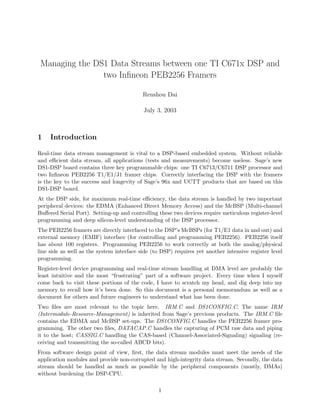
5.1 Relative pointer positions
In Figure 5, the memory blocks are drawn in a circular form. For normal operation, the Rx pointer
is leading IRM DLYBFS (defined in IRM.H file) ahead of the Tx pointer, whereas the DSP pointer
leads IRM DSPPOS (defined in IRM.H) ahead of the Tx pointer. For example, when then Tx
EDMA channel is transmitting data out of memory block 0 to the McBSP and then to the framer
chip, the Rx EDMA channel is receiving data from McBSP and placing them into the memory
block IRM DLYBFS. The DSP-CPU, on the other hand, is processing the received data at block
IRM DSPPOS, and after processing, replaces the data with the data that need to be transmitted
out if necessary. Within each memory, the data is de-interleaved so that IRM BFSZ number of
samples of a particular DS0 always occupies a contiguous section of memory. The DSP CPU
marches through the data channel by channel, and each channel contains IRM BFSZ number of
samples.
8
9. 5.2 Drop-Insert and Terminating modes
As implied in Figure 5, if the DSP-CPU is not performing any processing and generation on the
data, the EDMA Tx and Rx naturally loops the received data out with a fixed amount of delay that
is determined by IRM DLYBFS and IRM BFSZ. Presently, IRM DLYBFS=6, and IRM BFSZ=32,
and this amounts to a delay of 192 samples for each DS0 channel which is equivalent to 24 ms. This
is the default Drop-and-Insert and Monitor mode. All the data looping is handled by the EDMA
without the involvement of the DSP-CPU.
If a DS0 channel performs only receive-type of measurement, and it is in Drop-and-Insert mode,
then the received data is processed, but its content is not altered, and it will be looped out again
by the Tx. If the DS0 channel also involves transmit-type of test, then the received data will be
replaced with newly-generated data that will be sent out.
In terminating mode, the DSP-CPU will fill each DS0 channel with idle code (0x7f for T1 and 0x55
for E1) before TX pointer catches up if a certain DS0 channel does not involve any transmitting-
type of testing. So, terminating mode is actually more expensive to the DSP-CPU time, although
the idle-code filling itself is also done through the so-called QDMA (quick-DMA) process, the
DSP-CPU still has to initiate the QDMA request for each channel of each data block.
5.3 DSP jitter buffering
Figure 5 essentially shows this relationship: the DSP processing pointer is chasing the EDMA Rx
pointer, whereas the EDMA Tx is chasing the DSP pointer. Both the EDMA Rx and Tx pointers
are moving at a regular “hardware” pace (4 ms jumps one block, for example), since the data
movement is essentially paced by the framing pulse and clocks received at the McBSP. The DSP
processing pointer, however, may wander about between the EDMA Tx and Rx pointers, since
the DSP normally takes uneven amount of time to process and generate a new block of data. For
example, if the DSP needs to perform a 128-ms long FFT. For most data blocks, the DSP simply
buffers data (4 ms at a time), which takes insignificant amount of CPU time. But once 128 ms
data have been accumulated, the CPU may need 1 to 2 ms to perform the FFT. If all 24 channel
requires such FFT at the same time, it may take up to 24 to 48 ms. Ideally, DSP should finish
processing the 4 ms block of data in less than 4 ms. The situation just described amounts to
running-out-of-real-time. To combat such situation, the memory blocks between DSP pointer and
Tx pointer in Figure 5 serves as a jitter buffer. If once a while, the DSP-CPU takes more than 4
ms, but by average, uses less than 4 ms per block, then the jitter-buffering scheme in Figure 5 will
guarantee data integrity despite occasional real-time-over-use. As long as the DSP pointer leads
ahead the EDMA Tx pointer, there will be no data integrity issue. In Figure 5, the circular buffer
can tolerate up to IRM DSPPOS-1 block of real-time-over-use at a single moment.
6 Loss of frame or loss of signal
In either internal or external clock modes, the transmitting direction is always active and running
regardless whether or not the T1/E1 physical transmission line has been connected to another
equipment’s receiver. In Figure 5, the EDMA Tx pointer is always moving at the regular constant
pace counter-clock-wise.
The receive side, however, is completely a different story. The receiver operates differently depend-
9
10. ing on whether it is in-frame or out-of-frame.
6.1 Receiver in frame
If the PEB framer chip receives T1/E1 signal from another transmitting equipment and it is in
frame, then the EDMA Rx pointer in Figure 5 should move at similar constant regular pace as the
transmitter. This is the normal operation.
6.2 Receiver out of frame
If loss of frame or loss of signal occurs, then all the received data from PEB2256 to McBSP become
unreliable. Even worse, the framing pulse may arrive at a rate that is far different from the ideal
8000Hz rate. This essentially causes the EDMA Rx pointer in Figure 5 to move at an unpredictable
pace, and can cause corruption even to the transmitting data.
Under this situation, our design goal is to still guarantee the integrity of the transmitting data. For
example, if some user unplugs the wire out of the receive jack, the sending-tone test should still
function without any interruption, although the measure-tone test will be halted until valid signal
comes back again.
To achieve this goal, the following steps are taken: whenever loss of frame is detected by the framer
chip, the framer chip will issue an interrupt (PEB0 to EXT INT4 and PEB1 to EXT INT5) to
the DSP. Inside the interrupt service routine, the DSP simply shuts down the receive data stream
by disabling McBSP receive path. In this way, the erroneous framing pulses and data and clocks
from the PEB receive path are ignored, and the EDMA Rx path is automatically frozen since it is
dependent on the McBSP receive event. In Figure 5, the EDMA Rx pointer is essentially frozen,
but the DSP pointer and EDMA Tx pointer keep moving on as usual.
To make sure the active measurement-type tests (such as measure-tone) are not measuring bogus
data when the T1/E1 receiver loses frame, the block that is going to be processed by the DSP-CPU
is quickly filled with T1/E1 idle code (through QDMA process). This serves two purposes, first of
all, the measurement test is still functioning normally except it is measuring idle signal, secondly,
in drop-insert-mode, our transmitter will not dump out bogus data or keep recycling the recently
received IRM NBFS blocks of data. This idle code refilling is handled in IRM chkdata() function.
Details of this function will be explained later.
6.3 Frame loss recovery
When frame loss is recovered (PEB in frame again), the software procedure to restart the receiving
process is a bit more complicated.
First of all, upon re-framing, the PEB will issue another interrupt to the DSP. Inside the interrupt
service routine, the DSP not only re-enables the McBSP receive path, it also needs to re-position
the EDMA Rx pointer based on the current EDMA Tx pointer position. This is required so that
the circular memory blocks in Figure 5 still function according to design, and to a user, the drop-
insert mode presents a constant loop delay of 24 ms, for example. If this is not done, just imagine
the Rx pointer is “stuck” between the DSP pointer and the EDMA Tx pointer. All the new data
generated by the DSP that is meant to be transmitted out is in fact replaced by the newly received
data. To an operator, the equipment is running in a strange useless mode.
10
11. In essence, the EDMA Rx needs to be jump-started at a position that is IRM DLYBFS blocks
ahead of the current EDMA Tx position. This is all accomplished in the function IRM resync(),
called from the interrupt service routine. Inside the IRM resync, the current EDMA Tx position
is found by reading the PaRAM parameters associated with McBSP Tx0 or McBSP Tx1 as shown
in Figure 4. The position information is then used to calculate the ideal EDMA Rx position, and
the corresponding EDMA parameters are loaded in by the DSP-CPU. More specifically, the block
information (which block is EDMA Tx at now?) is determined by reading the chained-EDMA
position indicator. The finer position within a block is determined by reading out the frame and
element counter values out of the PaRAM active entry of EDMA Tx at entry 12 (PEB0) or entry
14 (PEB1).
So, keep in mind that, constant loss-of-framing and re-framing is quite disruptive to the data
stream.
7 Synchronizing DSP with the EDMA Tx
7.1 Detecting the availability of data
The ultimate goal of the EDMA’s movement of data between the circular memory buffer and
McBSP is for the DSP-CPU to use the data. As shown in Figure 5, the DSP-CPU performs the
“in-situ” operation on the data. That is, for receive type of measurement, the DSP analyzes the
block of data pointed by DSP processing pointer. If transmit type of test is also required for certain
channels, then the to-be-transmitted signal data is then written into the same block of memory.
Otherwise, in drop and insert mode, the data is not altered, hence to outsider, the DS1 connection
forms a natural loop-back. In terminating mode, the DSP will make sure idle code is filled in for
all the DS0 channels where transmitter type of tests are not specified.
As shown in Figure 4, each time a block of data has been moved in or out by the EDMA, the
EDMA will trigger a chained EDMA process. This chained EDMA will move from a naturally-
incrementing memory location with naturally-incrementing numbers from 0 to IRM NBFS-1 to a
fixed destination memory location associated with each of the 4 EDMA channels. The DSP-CPU
then reads (polls) whenever it can the destination memory location. From its content, the DSP-
CPU then knows when the EDMA Tx or Rx is. From the internal record of where EDMA TRx was
before, the DSP-CPU can deduce whether or not one or several blocks of data have been available
since last check.
Intuitively, as shown in Figure 5, the DSP-CPU should just check the EDMA Rx position, and
keeps following it. But unfortunately, the receiving DS1 path may always suffer the potential of
frame loss. When frame is lost, the receiving path is shutdown by shutting down the McBSP path
as discussed before. So the EDMA Rx is not a constant guide. The EDMA Tx, on the other hand, is
always running. Regardless whether or not the DS1 is in frame or out of frame, our test equipment
(from DSP point of view) will continue to send the required signal. So the data availability is in
fact based on the EDMA Tx position. But the EDMA Rx position is also being monitored to detect
any asynchronicity.
11
12. 7.2 Tx and Rx synchronicity
When the hardware is performing correctly, and in external mode, the EDMA Rx and EDMA Tx
should always be moving at the same pace at the block level at least (4 ms, for example), if not at
the bit level. So, they should never be out of synchronization from each other. In internal clock
mode, and if the equipment connected to ours is not clocked correctly (should be in external mode),
there might be some chance of out of synchronization. Regardless of the cause, when in frame,
the relative positions of the EDMA Tx and EDMA Rx are evaluated to detect any out-of-sync (up
to more than one block) situation . When it happens, it will call the IRM sync() function, whose
functionality has already been described before: the EDMA Rx position will jump-started to a new
position based on the current EDMA Tx position.
7.3 DSP real-time overuse
As shown in Figure 5, the DSP processing pointer should always lead ahead of the EDMA Tx
pointer. However, if the DSP-CPU is “stuck” in some real-time-intensive computation (hence the
DSP processing pointer stops moving while the EDMA Tx pointer keeps moving as usual), then
the Tx pointer will overlap or lead ahead of the DSP pointer. This signals that the DSP is running
out of real time. Whenever this is detected, the DSP-CPU will simply force the DSP processing
pointer to jump into the ideal location (IRM DSPPOS blocks ahead of EMDA Tx pointer), and then
reports to the host that DSP real-time overuse has occurred. This implies that the DSP application
modules have skipped over a block of signal. This will cause disruptions to all synchronous tests
that will be manifested as if a positive voice jitter (shortening of delay) has occurred.
The functionalities described above are implemented in the function IRM chkdata() function inside
the IRM.C file.
8 PCM audio capturing
The current 96x prototype also pipes some raw PCM data back to the host per demand. To
facilitate this feature, the DSP-CPU buffers up the selected DS0 data stream into a separate jitter
buffer whenever the DSP-CPU detects the availability of a new block of data. The data capturing
function is called from IRM chkdata(). A separate file DATACAP.C is created to handle this PCM
audio capturing feature.
A separate circular jitter buffer is needed because the incoming T1/E1 data stream arrives at a
regular pace (in 4 ms block by block right now). But the host requests the data (through, HPI and
USB) at an underterministic asynchronous fashion. A jitter buffer hence is needed to balance the
asynchronous natures the data streams at two sides. This is handled inside the DATACAP open()
and DATACAP transfer() functions.
Although the data copying itself is done through the CPU-initiated QDMA, the address calculations
and various management issues do cost quite a bit of CPU cycles, not to mention cost on USB-HPI
bandwidth and the host CPU time. The audio latency cannot be specified, and there is no way
to guarantee the quality (no dropping of packets). It is literally a best-effort approach. In the
final 96x product, when the embedded audio feature is implemented (through EDMA driven by the
framing pulses connected to the external interrupt pins 6 and 7 as briefly shown in Figure 4), this
inefficient approach should be abandoned, replaced with the more deterministic and low-latency
12
13. audio directly from the DSP.
9 CAS signaling bits
The CAS ABCD signaling bits also form part of the data stream, although it is handled in a
separate file CASSIG.C that is closely coupled with IRM.C and DS1CONFIG.C files.
There are three ways of accessing the ABCD signaling bits. The hardware approach requires using
the multi-purpose pins on the PEB2256 chip (RPA, RPB, RPC, RPD, XPA, XPB, XPC, XPD pins)
to transmit and receive the ABCD bits to and from the DSP-CPU. This requires some hardware
modifications, and also runs in conflict with the existing use of RPA and XPA as framing pulses
for the McBSP.
The second approach is purely based on software. Notice, in T1 mode, all 192 bits per frame is fed
to the DSP, and in E1 mode, the signaling time slot 16 is also fed to the DSP. So, theoretically,
the DSP should be able to detect the multi-frame boundary using some expansive bit-oriented
algorithms and then access the ABCD bits directly from the raw data stream. But this causes too
much waste on CPU real-time.
The third approach, which is the one used right now, is an interrupt and register based approach.
First of all, the ABCD signaling bits are readable from the PEB2256 registers RS1 to RS12 (T1
mode), and RS1 to RS16 (E1 mode). For transmitting, the bits should be written into the registers
XS1 to XS12 (T1) or XS16 (E1). The RSn and XSn registers actually share the same addresses.
When reading, the DSP-CPU does not blindly read the PEB registers. It is an interrupt-based ap-
proach. The interrupt associated with the signaling bits is enabled (implemented in DS1CONFIG.C
file). Whenever the framer chip detects a signaling bit change, it interrupts the DSP-CPU. When
responding to the interrupt, the DSP then reads the 12 or 16 RSn registers, and store the contents
in a separate DSP memory location. When the host requests the signaling bits information, the
DSP then analyzes the stored bits, and convert it to a form that is understandable by the host
(some amount of bit manipulations).
When transmitting, the DSP simply writes to the XSn registers. At the end, it writes a 1-bit into
the CASEN bit in the XSP register (E1) or the FMR5 register (T1). Both registers share the same
address.
References
[1] “TMS320C6000 Peripherals Reference Guide”, Texas Instruments Literature Number
SPRU190D, Feb., 2001.
[2] “FALC56 E1/T1/J1 Framer and Line Interface Component for Long and Short-Haul Applica-
tions, PEB 2256 Version 1.2”, Infineon data sheet, DS 2, October, 2001.
13
14. McBSP
FSR
Clock
Data
EDMA
Chained
EDMA
0
1
IRM_NBFS-1
EDMA
block
position
indicator
DSP
CPU
Data access
Data access
1 event
per 8-bit
1 event
per block
McBSP key settings:
1 phase per frame,
24/32 elements per frame,
8 bits per element
EDMA key settings:
element synced (FS=0),
element count=24/32,
frame count=IRM_BFSZ,
element index=24/32,
frame index=1-(elecnt-1)*frmcnt,
count reload and auto-link
Block 0
Block 1
IRM_NBFS-1
DS0 channel 0
channel 1
channel 23/31
PCM byte 0
byte 1
byte 2
IRM_BFSZ-1
Data memory details
Details within a block
Details within a channel
PaRAM setting details
PaRAM entry 0, addr=0x01a00000
entry 1, addr=0x01a00018
entry 12, McBSP0 xmit, link entry=16
entry 13, McBSP0 recv, link=16+IRM_NBFS
14, McBSP1 Tx, link=16+2*IRM_NBFS
15, McBSP1 Rx, link=16+3*IRM_NBFS
TCC8, chained to xmt0,link=16+4*IRM_NBFS
TCC9, chained to rcv0,link=17+4*IRM_NBFS
TCC10, chained to xmt1,link=18+4*IRM_NBFS
TCC11, chained to rcv1,link=19+4*IRM_NBFS
EXT_INT6, drive speaker, link=20+4*IRM_NBFS
EXT_INT7, drive mic, link=21+4*IRM_NBFS
entry 16, link=17
entry 17, link=18
entry 15+IRM_NBFS, link=16
entry 16+IRM_NBFS, link=17+IRM_NBFS
entry 17+IRM_NBFS, link=18+IRM_NBFS
entry 15+2*IRM_NBFS, link=16+2*IRM_NBFS
entry 16+2*IRM_NBFS, link=17+2*IRM_NBFS
entry 17+2*IRM_NBFS, link=18+2*IRM_NBFS
entry 15+3*IRM_NBFS, link=16+2*IRM_NBFS
entry 16+3*IRM_NBFS, link=17+3*IRM_NBFS
entry 17+3*IRM_NBFS, link=18+3*IRM_NBFS
entry 15+4*IRM_NBFS, link=16+3*IRM_NBFS
entry 16+4*IRM_NBFS, link=16+4*IRM_NBFS
entry 17+4*IRM_NBFS, link=17+4*IRM_NBFS
entry 18+4*IRM_NBFS, link=18+4*IRM_NBFS
entry 19+4*IRM_NBFS, link=19+4*IRM_NBFS
entry 20+4*IRM_NBFS, link=20+4*IRM_NBFS
entry 21+4*IRM_NBFS, link=21+4*IRM_NBFS
Figure 4: McBSP, EDMA, chained EDMA and DSP-CPU interconnections
14
15. block 0
1
channel 24/32
1
2
2
Block IRM_NBFS-1
IRM_DSPPOS
IRM_DLYBFS
TX pointer (EDMA TX)
RX pointer (EDMA RX)
DSP pointer
Direction of pointer movement
Figure 5: Relative pointer positions of the EDMA Tx and Rx and the DSP processing
pointer.
15