SlideShare a Scribd company logo
1 of 15
Download to read offline
1
Chapter Two
Diode Characteristics
2.1. PN Junction
2.2. Diode Operations
2.3. PN Diode as a Rectifier
2.4. Zener Diode Characteristics
2.5. LED and Photo Diode
2.1 PN Junction
The region where the block of p- type material is joined to a block of n- type material is called a
PN junction and is a fundamental component of many electronic devices, including diode,
transistors and others. Remember that diffusion current flows whenever there is a surplus of
carriers in one region and a corresponding lack of carriers of the same kind in another region.
Consequently, at the instant the P and N blocks are joined, electrons from the N region diffuse into
the P region, and holes from the P region diffuse into the N region. (Recall that this hole current is
actually the repositioning of holes due to the motion of valence band electrons.)
For each electron that leaves the N region to cross the junction into the P region, a donor atom that
now has a net positive charge is left behind. Similarly, for each hole that leaves the P region (that
is, for each acceptor atom that captures an electron), an acceptor atom acquires a net negative
charge. The upshot of this process is that negatively charged donor atoms accumulate just inside
the p region, and positively charged donor atoms accumulate just inside the N region. This charge
distribution often called space charge.
Depletion region
Figure 2.1: The PN junction showing charged ions after hole and electron diffusion
Δ’
P N
Hole
Electron
2
It is well known that accumulation of electric charge of opposite polarities in two separated regions
cause an electric field to be established between those regions. The accumulation of positive ions
in N material and negative ions in the P material established an electric field across a PN junction.
The direction of field is from the positive N region to the negative P region. Figure 2.1 illustrates
the field Δ’ developed across a PN junction.
The accumulation of negative charge in the p region prevents additional negative charge from
entering that region (like charges repel each other) and, similarly, the positively charged N region
repels additional positive charge. Therefore, after the initial surge of charge across the junction,
the diffusion current dwindles (becoming gradually less) to a negligible amount.
The direction of electric field across the PN junction enables the flow of drift current from the P
to the N region, that is, the flow of electrons from left to right and of holes from right to left, in
figure 2.1. There is therefore a small drift of minority carriers in opposite direction from the
diffusion current. When equilibrium condition has been established, the small reverse drift current
exactly cancels the diffusion current from N to P. the net current across the junction is therefore
zero.
Remember that the P-region holes have been annihilated by electrons, and the N-region electrons
have migrated to the P side. Because all charge carriers have been depleted (removed) from this
region, it is called the depletion region. It is also called barrier region because the electric field
their acts as a barrier to further diffusion current.
The values of barrier potential, VO, depends on the doping levels in the P and N regions, the type
of material (Si and Ge), and the temperature.
VO =
𝐾𝑇
π‘ž
ln
𝑁𝐴 𝑁𝐷
𝑛𝑖2 (2.1)
Where, VO = barrier potential,
K = Boltzmann’s constant = 1.38 Γ— 10βˆ’23
J/0
k,
T = temperature of the material in Kelvin (0
k = 273 + 0
c),
q = electron charge = 1.6 Γ— 10βˆ’19
c
NA = acceptor doping density in the P material,
ND = donor doping density in the N material
3
𝑛𝑖 = intrinsic electron density.
VT =
KT
q
(2.2)
Where, VT = thermal voltage
2.1.1 Forward – biased junction
When an external dc source is connected across a PN junction, the polarity of the connection can
be such that it either opposes or reinforces the barrier. Suppose a voltage source VD is connected
as shown in figure-2.2, with its positive terminal attached to the P side of a PN junction and its
negative terminal attached to the N side. With polarity of connections shown in the figure 2.2, the
external source creates an electric field component across the junction whose direction opposes
the internal field established by the space charge.
In other words, the barrier is reduced, so diffusion current is enhanced. Therefore, current flows
with relative ease through the junction, its direction of flow is from P to N, as shown in figure 2.2.
In this case the junction is said to be forward biased.
h = hole; Δ“ = electron
Figure 2.2: Forward-biased p-n junction, Narrow depletion width
When the PN junction is forward biased, electrons are forced into the N region by the external
source and holes are forced into the P region. As free electrons move toward the junction through
the N material, a corresponding number of holes progresses through the P material. Thus, current
in each region is the result of majority carrier flow. Electrons diffuse through the depletion region
and recombine with holes in the P material. For each hole that recombines with an electron, an
electron from a covalent bond leaves the P region and enters the positive terminal of the external
source, thus maintaining the equality of current entering and leaving the source. Since there is a
reduction in the electric field barrier at the forward- biased junction, there is a corresponding
Δ’
h Δ“
4
reduction in the quantity of ionized acceptor and donor atoms required to maintain the field. As a
result, the depletion region narrows under forward bias.
2.1.2 Reverse - biased junction
When the positive terminal of the source is connected to the N side of the junction and the negative
terminal is connected to the P side (shown in figure 2.3) the polarity of the bias voltage reinforces,
or strengthens, the internal barrier field at the junction. Consequently, diffusion current is inhibited
to an even greater extent than it was with no bias applied. The increased field intensity must be
supported by an increase in the number of ionized donor and acceptor atoms, so the depletion
regions widen under reverse bias.
Figure 2.3: Reverse - biased p-n junction, wide depletion region
Recall that, the unbiased PN junction has a component of drift current consisting of minority
carriers that cross the junction from the P to the N side. This reverse current is the direct result of
the electric field across the depletion region. Since a reverse – biasing voltage increases the
magnitude of that field, we can expect the reverse current to increases correspondingly. The current
magnitude is very much smaller than the current that flows under forward bias.
The distinction between the ways a PN junction reacts to a bias voltage, very little current flow
when it is reverse biased and substantial current flow when it is forward biased, makes it very
useful device in many circuit applications.
2.2 Diode operation
Diode is made up of a small piece of semiconductor material, usually silicon, in which half is
doped as a p region and half is doped as an n region with a pn junction and depletion region in
between. The p region is called the anode and is connected to a conductive terminal. The n region
5
is called the cathode and is connected to a second conductive terminal. The basic diode structure
and schematic symbol are shown in Figure 2–4 given below.
Figure 2.4 schematic symbol of diode.
2.2.1 Characteristics of ideal & practical diode
Understanding the operation of the semiconductor diode is the basis for an understanding of all
semiconductor devices. It is the simplest of semiconductor devices but plays a very vital role in
electronic systems, having characteristics that closely match those of a simple switch. The term
ideal refers to any device or system that has ideal characteristics perfect in every way. The ideal
diode is a two-terminal device having the symbol and characteristics shown in figure 2.5, a and b
respectively. The characteristics of an ideal diode are those of a switch that can conduct current in
only one direction.
Figure 2.5 Conduction (a) and non-conduction (b) state of Ideal diode
The P side of the diode is called its anode and the N side is called its cathode.
ID = IS (𝑒
𝑉𝐷
πœ‚π‘‰π‘‡ βˆ’ 1) (2.3)
ID = current; VD = voltage (positive for forward bias and negative for reverse bias).
IS = saturation current; Ξ· = emission coefficient; VT = thermal voltage.
6
Figure 2.6: I-V relations in a PN junction under forward and reverse bias
1) A silicon diode has a reverse saturation current of 7.12nA at room temperature of 27oc.
Calculate its forward current if it is forward biased with a voltage of 0.7v.
Solution: The given values are
Is = 7.2nA, K=1.38*10e-23 J/K, Q = 1.6*10-19 C
V = + 0.7 v as forward biased.
πœ‚ = 2 for silicon diode
T = 270
𝐢 = 27 + 273 = 3000
𝐾
Now VT = KT/q = 8.62 x 10-5 x 300 = 0.026 v
Using diode current equation,
I = 4.99 x 10⁻³A = 5mA. Thus, the forward current is 5mA.
I) The Ideal Diode Model
The ideal model of a diode is the least accurate approximation and can be represented by a simple
switch as shown in the figure 2.7 below.
Figure 2.7 V-I characteristics of ideals diodes
7
When the diode is forward-biased, it ideally acts like a closed (on) switch, as shown in Figure 2.7
(a). When the diode is reverse-biased, it ideally acts like an open (off) switch, as shown in part (b).
In Figure 2.7 (c), the ideal V-I characteristic curve graphically depicts the ideal diode operation.
II) The Practical Diode Model
The practical model includes the barrier potential. When the diode is forward-biased, it is
equivalent to a closed switch in series with a small equivalent voltage source (VF) equal to the
barrier potential (0.7 V) with the positive side toward the anode, as indicated in Figure 2.8 (a).
This equivalent voltage source represents the barrier potential that must be exceeded by the bias
voltage before the diode will conduct and is not an active source of voltage. When conducting, a
voltage drop of 0.7 V appears across the diode. When the diode is reverse-biased, it is equivalent
to an open switch just as in the ideal model, as shown in Figure 2.8 (b). The barrier potential does
not affect reverse bias, so it is not a factor. The characteristic curve for the practical diode model
is shown in Figure 2.8 (c).
Figure 2.8 V-I characteristics of practical diodes
2.2.2 Breakdown
The reverse current also deviates from that predicted by the ideal diode equation if the reverse
biasing voltage is allowed to approach a certain value called the reverse break down voltage, VBR.
A very small increase in reverse bias voltage in the vicinity of VBR results in a very large increase
in reverse current. In other word the diode no longer exhibits its normal characteristics of
maintaining a very small, essentially constant reverse current with increasing reverse voltage.
8
Figure 2.9: a plot of the I-V relation for diode, showing the sudden increase in reverse current
near the reverse break down voltage.
In ordinary diodes, the breakdown phenomenon occurs because the high electric field in the
depletion region impart high kinetic energy (large velocities) to the carriers crossing the region,
and when these carriers collide with other atoms, they rupture covalent bonds.
The large numbers of carriers that are freed in this way accounts for the increase in reverse current
through the junction. The process is called avalanching. The magnitude of the reverse current that
flows when V approaches VBR can be predicted from the relation:
I =
IS
1βˆ’[
𝑉
𝑉𝐡𝑅
]𝑛
(2.4)
Where n is a constant determined by experiment and has a value between 2 and 6.
The value of the breakdown voltage depends on doping and other physical characteristics that are
controlled in manufacturing. Ordinary diodes may have breakdown voltage ranging from 10 or 20
to hundreds of volts.
2.3 Diode as a Rectifier
Almost all electronics circuits require a dc source of power. For portable low power systems
batteries may be used. More frequently electronic equipment is energized by a power supply, a
piece of equipment which converts the alternating waveform from the power lines into an essential
direct voltage. A device, such as the semiconductor diode, which is capable of converting a
sinusoidal input waveform (whose average value is zero) into a unidirectional waveform, with a
nonzero average component, is called a rectifier. The process of converting AC to DC waveform
is called rectifications. There are two types of rectifications process:
2.3.1 Half-wave rectification
In half-wave rectification either the positive or negative half of the ac wave is passed, while the
other half is blocked. The basic circuit for half – wave rectification is shown in figure 2.10.
9
Figure 2.10: Half-wave rectifier
Over one full cycle, defined by the period T of figure 2.10, the average value (the algebraic sum
of the areas above and below the axis) of vi is zero.
During the interval t = 0 β†’ T/2 in figure 2.10 the polarity of the applied voltage vi is such as to
establish β€œpressure” in the direction indicated and turn on the diode with the polarity appearing
above the diode. Substituting the short-circuit equivalence for the ideal diode will result in the
equivalent circuit of figure 2.11, where it is fairly obvious that the output signal is an exact replica
of the applied signal. The two terminals defining the output voltage are connected directly to the
applied signal via the short-circuit equivalence of the diode.
Figure 2.11: Conduction region (0β†’ T/2)
For the period T/2 β†’ T, the polarity of the input vi is as shown in figure 2.12 and the resulting
polarity across the ideal diode produces an β€œoff” state with an open-circuit equivalent. The result
is the absence of a path for charge to flow and vo = iR = (0) *R = 0 V for the period T/2 β†’ T. The
input vi and the output vo were sketched together in figure 2.13 for comparison purposes.
10
Figure 2.12: Non-conduction region
The output signal vo now has a net positive area above the axis over a full period and an average
value determined by:
Vdc = 0.318𝑉
π‘š (2.5)
Figure 2.13: Half-wave rectified signal
Note that the net effect of half – wave circuit is the conversion of an ac voltage into a (pulsating)
dc voltage.
The effect of using a silicon diode with VT = 0.7 V is demonstrated in figure 2.14 for the forward-
bias region. The applied signal must now be at least 0.7 V before the diode can turn β€œon.” For
levels of vi less than 0.7 V, the diode is still in an open-circuit state and vo = 0 V as shown in the
same figure. When conducting, the difference between vo and vi is a fixed level of VT = 0.7 V and
vo = vi βˆ’ VT, as shown in the figure 2.14. The net effect is a reduction in area above the axis, which
naturally reduces the resulting dc voltage level.
Figure 2.14: Effect of VT on Half-wave rectified signal
11
For situations where Vm ≫ VT, the average value is determined by Eq.2.6.
𝑉𝑑𝑐 β‰… 0.318(𝑉
π‘š βˆ’ 𝑉𝑇 ) (2.6)
The peak inverse voltage (PIV) [or PRV (peak reverse voltage)] rating of the diode is the voltage
rating that must not be exceeded in the reverse-bias region or the diode will enter the Zener
avalanche region. The required PIV rating for the half-wave rectifier can be determined in Eq.2.7.
π‘ƒπΌπ‘‰π‘Ÿπ‘Žπ‘‘π‘–π‘›π‘” β‰₯ 𝑉
π‘š (2.7)
2.3.2 Full - wave rectification
A full – wave rectifier effectively inverts the negative half – pulses of a sine wave to produce an
output that is a sequence of positive half – pulses with no intervals between them. It is more
efficient than the half – wave rectifier.
The dc level (average value) obtained from a sinusoidal input can be improved 100% using a
process called full – wave rectification.
Bridge network: it is the most familiar network for performing a full – wave rectification. It is
shown in figure 2.15 with its four diodes in a bridge configuration.
Figure 2.15: Full – wave bridge rectifier
During the period t = 0 to T/2 the polarity of the input is as shown in figure 2.16a. The resulting
polarities across the ideal diodes are also shown in figure 2.16a to reveal that D2 and D3 are
conducting while D1 and D4 are in the β€œoff” state. The net result is the configuration of figure
2.16b, with its indicated current and polarity across R. Since the diodes are ideal the load voltage
is vo = vi, as shown in the same figure.
12
Figure 2.16: (a) Network of figure 2.15 for the period 0 β†’T/2 of the input voltage vi. (b)
Conduction path for the positive region of vi
For the negative region of the input the conducting diodes are D1 and D4, resulting in the
configuration of figure 2.17. The important result is that the polarity across the load resistor R is
the same as in figure 2.16a, establishing a second positive pulse, as shown in figure 2.17.
Figure 2.17: Conduction path for the negative region of vi
Over one full cycle the input and output voltages will appear as shown in figure 2.18. Since the
area above the axis for one full cycle is now twice that obtained for a half-wave system, the dc
level has also been doubled.
𝑉𝑑𝑐 = 0.636𝑉
π‘š (2.8)
Figure 2.18: input and output waveform for a full-wave rectifier
If silicon rather than ideal diodes is employed as shown in figure 2.19, an application of
Kirchhoff’s voltage law around the conduction path would result in
𝑣𝑖 βˆ’ 𝑉𝑇 βˆ’ π‘£π‘œ βˆ’ 𝑉𝑇 = 0
13
π‘£π‘œ = 𝑣𝑖 βˆ’ 2𝑉𝑇
The peak value of the output voltage vo is therefore
𝑉
π‘œπ‘šπ‘Žπ‘₯
= 𝑉
π‘š βˆ’ 2𝑉𝑇
For situation where Vm≫ 2VT the average value is determined by Eq.2.9
𝑉𝑑𝑐 β‰… 0.636 (𝑉
π‘š βˆ’2𝑉𝑇) (2.9)
Figure 2.19: Determining 𝑉
π‘œπ‘šπ‘Žπ‘₯
for silicon diodes in the bridge configuration
𝑃𝐼𝑉
π‘“π‘’π‘™π‘™βˆ’π‘€π‘Žπ‘£π‘’ π‘π‘Ÿπ‘–π‘‘π‘”π‘’ π‘Ÿπ‘’π‘π‘‘π‘–π‘“π‘–π‘’π‘Ÿ β‰₯ 𝑉
π‘š (2.10)
2.4 Zener diode
Zener diode is a reverse-biased heavily doped p-n junction diode which is operated in the
breakdown region. The symbol of a Zener diode is shown in figure 2.20a. It is like an ordinary p-
n junction diode except that it is properly doped so as to have a sharp breakdown voltage. When
forward biased, its characteristics are similar to that of an ordinary diode. It is always reverse
biased and has sharp breakdown voltage, called the Zener voltage. By controlling the junction
width and doping densities of diode it is possible to make it to breakdown at a sharp specified
Zener voltage from about 2 to 200 V. A Zener diode is specified by its breakdown voltage and the
maximum power dissipation.
Figure 2.20: (a) Zener diode, (b) the normal operation region of Zener diode is shaded
14
The most common application of a Zener diode is the voltage stabilization. The Zener diode in
breakdown maintains an almost constant voltage across itself over a wide current range. The
complete equivalent circuit of the Zener diode in the Zener region includes a small dynamic
resistance and dc battery equal to the Zener potential, as shown in figure 2.21.
For all applications to follow, however, we shall assume as a first approximation that the external
resistors are much larger in magnitude than the Zener-equivalent resistor and that the equivalent
circuit is simply the one indicated in figure 2.21b.
Figure 2.21: Zener equivalent circuit (a) complete (b) approximate
Zener diodes are most frequently used in regulator networks or as a reference voltage.
2.5 LED, LCD and Photo Diode
2.5.1 Light - Emitting Diodes
The increasing use of digital displays in calculators, watches, and all forms of instrumentation has
contributed to the current extensive interest in structures that will emit light when properly biased.
The two types in common use today to perform this function are the light-emitting diode (LED)
and the liquid-crystal display (LCD). As the name implies, the light-emitting diode (LED) is a
diode that will give off visible light when it is energized. In any forward-biased p-n junction there
is, within the structure and primarily close to the junction, a recombination of holes and electrons.
This recombination requires that the energy possessed by the unbound free electron be transferred
to another state.
In all semiconductor p-n junctions some of this energy will be given off as heat and some in the
form of photons. In silicon and germanium, the greater percentage is given up in the form of heat
and the emitted light is insignificant. In other materials, such as gallium arsenide phosphide
(GaAsP) or gallium phosphide (GaP), the number of photons of light energy emitted is sufficient
15
to create a very visible light source. The process of giving off light by applying an electrical source
of energy is called electroluminescence.
As shown in figure below with its graphic symbol, the conducting surface connected to the p-
material is much smaller, to permit the emergence of the maximum number of photons of light
energy. Note in the figure that the recombination of the injected carriers due to the forward-biased
junction results in emitted light at the site of recombination. There may, of course, be some
absorption of the packages of photon energy in the structure itself, but a very large percentage are
able to leave, as shown in figure.
Figure 2.22: (a) Process of electroluminescence in the LED; (b) graphic symbol
2.5.2 Photodiodes
While LEDs emit light, Photodiodes are sensitive to received light. They are constructed so their
p-n junction can be exposed to the outside through a clear window or lens. In Photoconductive
mode the saturation current increases in proportion to the intensity of the received light. This type
of diode is used in CD players. In Photovoltaic mode, when the p-n junction is exposed to a certain
wavelength of light, the diode generates voltage and can be used as an energy source. This type of
diode is used in the production of solar power.
Figure 2.23: Schematic symbols for photodiodes

More Related Content

What's hot

P n junction characteristics
P n junction characteristicsP n junction characteristics
P n junction characteristicsAshvani Shukla
Β 
Diode Applications & Transistor Basics
Diode Applications & Transistor BasicsDiode Applications & Transistor Basics
Diode Applications & Transistor BasicsA B Shinde
Β 
Pn junction diodes (presentation)
Pn junction diodes (presentation)Pn junction diodes (presentation)
Pn junction diodes (presentation)Alan Bullard
Β 
Pn junction diode class 12 investegatory project
Pn junction diode class 12 investegatory projectPn junction diode class 12 investegatory project
Pn junction diode class 12 investegatory projectabhijeet singh
Β 
Rec101 unit 1 (part ii) pn junction diode
Rec101 unit 1 (part ii)  pn junction diodeRec101 unit 1 (part ii)  pn junction diode
Rec101 unit 1 (part ii) pn junction diodeDr Naim R Kidwai
Β 
[FULL ANIMATED(Download to view)] Unbiased diode, Forward biased , reverse bi...
[FULL ANIMATED(Download to view)] Unbiased diode, Forward biased , reverse bi...[FULL ANIMATED(Download to view)] Unbiased diode, Forward biased , reverse bi...
[FULL ANIMATED(Download to view)] Unbiased diode, Forward biased , reverse bi...Pratik Nakrani
Β 
Semi conductor diode
Semi conductor diodeSemi conductor diode
Semi conductor diodeSidharth Sharma
Β 
Semiconductor diode
Semiconductor diodeSemiconductor diode
Semiconductor diodeAnsari Maviya
Β 
P n junction diode
P n junction diodeP n junction diode
P n junction diodeHarsh Vijay
Β 
BASIC ELECTRONICS , By Ritwik Tripathi Dept Of EEE, Dr. C.V.Raman University
BASIC ELECTRONICS , By Ritwik Tripathi Dept Of EEE, Dr. C.V.Raman UniversityBASIC ELECTRONICS , By Ritwik Tripathi Dept Of EEE, Dr. C.V.Raman University
BASIC ELECTRONICS , By Ritwik Tripathi Dept Of EEE, Dr. C.V.Raman UniversityRana Sharma
Β 
EST 130, PN Junction Diodes
EST 130, PN Junction DiodesEST 130, PN Junction Diodes
EST 130, PN Junction DiodesCKSunith1
Β 
Patrick Henry Entropic - Characteristics of Semiconductor Diode
Patrick Henry Entropic - Characteristics of Semiconductor DiodePatrick Henry Entropic - Characteristics of Semiconductor Diode
Patrick Henry Entropic - Characteristics of Semiconductor DiodePatrick Henry Entropic
Β 
Pn diode presentation
Pn diode presentationPn diode presentation
Pn diode presentationBilawal Fiaz
Β 
Semiconductor diode
Semiconductor diodeSemiconductor diode
Semiconductor diodesushil sirsat
Β 
Diodes and rectifiers
Diodes and rectifiersDiodes and rectifiers
Diodes and rectifiersAnkit Dubey
Β 
Semiconductor diodes
Semiconductor diodesSemiconductor diodes
Semiconductor diodespriyanka singh
Β 
BASIC ELECTRONICS!!
BASIC ELECTRONICS!!BASIC ELECTRONICS!!
BASIC ELECTRONICS!!Daniel Musyoka
Β 

What's hot (20)

P n junction characteristics
P n junction characteristicsP n junction characteristics
P n junction characteristics
Β 
Diode Applications & Transistor Basics
Diode Applications & Transistor BasicsDiode Applications & Transistor Basics
Diode Applications & Transistor Basics
Β 
Pn junction diodes (presentation)
Pn junction diodes (presentation)Pn junction diodes (presentation)
Pn junction diodes (presentation)
Β 
Pn junction diode class 12 investegatory project
Pn junction diode class 12 investegatory projectPn junction diode class 12 investegatory project
Pn junction diode class 12 investegatory project
Β 
Rec101 unit 1 (part ii) pn junction diode
Rec101 unit 1 (part ii)  pn junction diodeRec101 unit 1 (part ii)  pn junction diode
Rec101 unit 1 (part ii) pn junction diode
Β 
[FULL ANIMATED(Download to view)] Unbiased diode, Forward biased , reverse bi...
[FULL ANIMATED(Download to view)] Unbiased diode, Forward biased , reverse bi...[FULL ANIMATED(Download to view)] Unbiased diode, Forward biased , reverse bi...
[FULL ANIMATED(Download to view)] Unbiased diode, Forward biased , reverse bi...
Β 
Semi conductor diode
Semi conductor diodeSemi conductor diode
Semi conductor diode
Β 
beee ppt upload
 beee ppt upload beee ppt upload
beee ppt upload
Β 
PN JUNCTION
PN JUNCTIONPN JUNCTION
PN JUNCTION
Β 
Semiconductor diode
Semiconductor diodeSemiconductor diode
Semiconductor diode
Β 
P n junction diode
P n junction diodeP n junction diode
P n junction diode
Β 
BASIC ELECTRONICS , By Ritwik Tripathi Dept Of EEE, Dr. C.V.Raman University
BASIC ELECTRONICS , By Ritwik Tripathi Dept Of EEE, Dr. C.V.Raman UniversityBASIC ELECTRONICS , By Ritwik Tripathi Dept Of EEE, Dr. C.V.Raman University
BASIC ELECTRONICS , By Ritwik Tripathi Dept Of EEE, Dr. C.V.Raman University
Β 
EST 130, PN Junction Diodes
EST 130, PN Junction DiodesEST 130, PN Junction Diodes
EST 130, PN Junction Diodes
Β 
Patrick Henry Entropic - Characteristics of Semiconductor Diode
Patrick Henry Entropic - Characteristics of Semiconductor DiodePatrick Henry Entropic - Characteristics of Semiconductor Diode
Patrick Henry Entropic - Characteristics of Semiconductor Diode
Β 
Pn diode presentation
Pn diode presentationPn diode presentation
Pn diode presentation
Β 
Semiconductor diode
Semiconductor diodeSemiconductor diode
Semiconductor diode
Β 
Diode
DiodeDiode
Diode
Β 
Diodes and rectifiers
Diodes and rectifiersDiodes and rectifiers
Diodes and rectifiers
Β 
Semiconductor diodes
Semiconductor diodesSemiconductor diodes
Semiconductor diodes
Β 
BASIC ELECTRONICS!!
BASIC ELECTRONICS!!BASIC ELECTRONICS!!
BASIC ELECTRONICS!!
Β 

Similar to Chap 2

Electronics ichapter1
Electronics ichapter1Electronics ichapter1
Electronics ichapter1Ankit Dubey
Β 
AE UNIT I.ppt
AE UNIT I.pptAE UNIT I.ppt
AE UNIT I.pptArunS118525
Β 
EC8252-Electronic Devices Question Bank.pdf
EC8252-Electronic Devices Question Bank.pdfEC8252-Electronic Devices Question Bank.pdf
EC8252-Electronic Devices Question Bank.pdfRajaSekaran923497
Β 
Minor project report on pn junction, zener diode, led characteristics
Minor project report on pn junction, zener diode, led characteristicsMinor project report on pn junction, zener diode, led characteristics
Minor project report on pn junction, zener diode, led characteristicsom prakash bishnoi
Β 
Electronics Engineering Diode , Transistor ,BJT
Electronics Engineering Diode , Transistor ,BJTElectronics Engineering Diode , Transistor ,BJT
Electronics Engineering Diode , Transistor ,BJTyadavsuyash008
Β 
pn-junctiondiodeJJNINIIJOIOOIMOMOKMOMOIM
pn-junctiondiodeJJNINIIJOIOOIMOMOKMOMOIMpn-junctiondiodeJJNINIIJOIOOIMOMOKMOMOIM
pn-junctiondiodeJJNINIIJOIOOIMOMOKMOMOIMSaravanan Pazapughal
Β 
227 sample chapter
227 sample chapter227 sample chapter
227 sample chapterAnkit Dubey
Β 
CA1-ELECTRONICS ENGINEERING ON PN JUNCTION.pdf
CA1-ELECTRONICS ENGINEERING ON PN JUNCTION.pdfCA1-ELECTRONICS ENGINEERING ON PN JUNCTION.pdf
CA1-ELECTRONICS ENGINEERING ON PN JUNCTION.pdfsumansafui97
Β 
PN Junction.pptx
PN Junction.pptxPN Junction.pptx
PN Junction.pptxAsifRahaman16
Β 
A BASIC INTRODUCTION TO SEMICONDUCTOR DEVICES - THE
A BASIC INTRODUCTION TO SEMICONDUCTOR DEVICES - THEA BASIC INTRODUCTION TO SEMICONDUCTOR DEVICES - THE
A BASIC INTRODUCTION TO SEMICONDUCTOR DEVICES - THEWinston Bent A.S.S.
Β 
BEEIE UNIT IV PPT.ppt
BEEIE UNIT IV PPT.pptBEEIE UNIT IV PPT.ppt
BEEIE UNIT IV PPT.pptDEEBIKAR2
Β 
Type of pn junction & rectifiers plus Transistor
Type of pn junction & rectifiers plus TransistorType of pn junction & rectifiers plus Transistor
Type of pn junction & rectifiers plus TransistorMuhammad Adeel Shakir
Β 
Physics project
Physics projectPhysics project
Physics projectsubrat singh
Β 

Similar to Chap 2 (20)

Electronics ichapter1
Electronics ichapter1Electronics ichapter1
Electronics ichapter1
Β 
AE UNIT I.ppt
AE UNIT I.pptAE UNIT I.ppt
AE UNIT I.ppt
Β 
EC8252-Electronic Devices Question Bank.pdf
EC8252-Electronic Devices Question Bank.pdfEC8252-Electronic Devices Question Bank.pdf
EC8252-Electronic Devices Question Bank.pdf
Β 
Chapter2
Chapter2Chapter2
Chapter2
Β 
Minor project report on pn junction, zener diode, led characteristics
Minor project report on pn junction, zener diode, led characteristicsMinor project report on pn junction, zener diode, led characteristics
Minor project report on pn junction, zener diode, led characteristics
Β 
Electronics Engineering Diode , Transistor ,BJT
Electronics Engineering Diode , Transistor ,BJTElectronics Engineering Diode , Transistor ,BJT
Electronics Engineering Diode , Transistor ,BJT
Β 
pn-junctiondiodeJJNINIIJOIOOIMOMOKMOMOIM
pn-junctiondiodeJJNINIIJOIOOIMOMOKMOMOIMpn-junctiondiodeJJNINIIJOIOOIMOMOKMOMOIM
pn-junctiondiodeJJNINIIJOIOOIMOMOKMOMOIM
Β 
BEEE.pptx
BEEE.pptxBEEE.pptx
BEEE.pptx
Β 
227 sample chapter
227 sample chapter227 sample chapter
227 sample chapter
Β 
Theory of solids
Theory of solidsTheory of solids
Theory of solids
Β 
CA1-ELECTRONICS ENGINEERING ON PN JUNCTION.pdf
CA1-ELECTRONICS ENGINEERING ON PN JUNCTION.pdfCA1-ELECTRONICS ENGINEERING ON PN JUNCTION.pdf
CA1-ELECTRONICS ENGINEERING ON PN JUNCTION.pdf
Β 
PN Junction.pptx
PN Junction.pptxPN Junction.pptx
PN Junction.pptx
Β 
A BASIC INTRODUCTION TO SEMICONDUCTOR DEVICES - THE
A BASIC INTRODUCTION TO SEMICONDUCTOR DEVICES - THEA BASIC INTRODUCTION TO SEMICONDUCTOR DEVICES - THE
A BASIC INTRODUCTION TO SEMICONDUCTOR DEVICES - THE
Β 
BEEIE UNIT IV PPT.ppt
BEEIE UNIT IV PPT.pptBEEIE UNIT IV PPT.ppt
BEEIE UNIT IV PPT.ppt
Β 
Pn junction diode
Pn junction diodePn junction diode
Pn junction diode
Β 
Type of pn junction & rectifiers plus Transistor
Type of pn junction & rectifiers plus TransistorType of pn junction & rectifiers plus Transistor
Type of pn junction & rectifiers plus Transistor
Β 
Edcqnaunit 8
Edcqnaunit 8Edcqnaunit 8
Edcqnaunit 8
Β 
Physics project
Physics projectPhysics project
Physics project
Β 
Edc unit 8
Edc unit 8Edc unit 8
Edc unit 8
Β 
Lec-2.pdf
Lec-2.pdfLec-2.pdf
Lec-2.pdf
Β 

Recently uploaded

Artificial-Intelligence-in-Electronics (K).pptx
Artificial-Intelligence-in-Electronics (K).pptxArtificial-Intelligence-in-Electronics (K).pptx
Artificial-Intelligence-in-Electronics (K).pptxbritheesh05
Β 
microprocessor 8085 and its interfacing
microprocessor 8085  and its interfacingmicroprocessor 8085  and its interfacing
microprocessor 8085 and its interfacingjaychoudhary37
Β 
HARMONY IN THE HUMAN BEING - Unit-II UHV-2
HARMONY IN THE HUMAN BEING - Unit-II UHV-2HARMONY IN THE HUMAN BEING - Unit-II UHV-2
HARMONY IN THE HUMAN BEING - Unit-II UHV-2RajaP95
Β 
Model Call Girl in Narela Delhi reach out to us at πŸ”8264348440πŸ”
Model Call Girl in Narela Delhi reach out to us at πŸ”8264348440πŸ”Model Call Girl in Narela Delhi reach out to us at πŸ”8264348440πŸ”
Model Call Girl in Narela Delhi reach out to us at πŸ”8264348440πŸ”soniya singh
Β 
Oxy acetylene welding presentation note.
Oxy acetylene welding presentation note.Oxy acetylene welding presentation note.
Oxy acetylene welding presentation note.eptoze12
Β 
Biology for Computer Engineers Course Handout.pptx
Biology for Computer Engineers Course Handout.pptxBiology for Computer Engineers Course Handout.pptx
Biology for Computer Engineers Course Handout.pptxDeepakSakkari2
Β 
CCS355 Neural Network & Deep Learning UNIT III notes and Question bank .pdf
CCS355 Neural Network & Deep Learning UNIT III notes and Question bank .pdfCCS355 Neural Network & Deep Learning UNIT III notes and Question bank .pdf
CCS355 Neural Network & Deep Learning UNIT III notes and Question bank .pdfAsst.prof M.Gokilavani
Β 
CCS355 Neural Network & Deep Learning Unit II Notes with Question bank .pdf
CCS355 Neural Network & Deep Learning Unit II Notes with Question bank .pdfCCS355 Neural Network & Deep Learning Unit II Notes with Question bank .pdf
CCS355 Neural Network & Deep Learning Unit II Notes with Question bank .pdfAsst.prof M.Gokilavani
Β 
Software and Systems Engineering Standards: Verification and Validation of Sy...
Software and Systems Engineering Standards: Verification and Validation of Sy...Software and Systems Engineering Standards: Verification and Validation of Sy...
Software and Systems Engineering Standards: Verification and Validation of Sy...VICTOR MAESTRE RAMIREZ
Β 
IVE Industry Focused Event - Defence Sector 2024
IVE Industry Focused Event - Defence Sector 2024IVE Industry Focused Event - Defence Sector 2024
IVE Industry Focused Event - Defence Sector 2024Mark Billinghurst
Β 
Application of Residue Theorem to evaluate real integrations.pptx
Application of Residue Theorem to evaluate real integrations.pptxApplication of Residue Theorem to evaluate real integrations.pptx
Application of Residue Theorem to evaluate real integrations.pptx959SahilShah
Β 
Sachpazis Costas: Geotechnical Engineering: A student's Perspective Introduction
Sachpazis Costas: Geotechnical Engineering: A student's Perspective IntroductionSachpazis Costas: Geotechnical Engineering: A student's Perspective Introduction
Sachpazis Costas: Geotechnical Engineering: A student's Perspective IntroductionDr.Costas Sachpazis
Β 
Microscopic Analysis of Ceramic Materials.pptx
Microscopic Analysis of Ceramic Materials.pptxMicroscopic Analysis of Ceramic Materials.pptx
Microscopic Analysis of Ceramic Materials.pptxpurnimasatapathy1234
Β 
Call Girls Delhi {Jodhpur} 9711199012 high profile service
Call Girls Delhi {Jodhpur} 9711199012 high profile serviceCall Girls Delhi {Jodhpur} 9711199012 high profile service
Call Girls Delhi {Jodhpur} 9711199012 high profile servicerehmti665
Β 
Past, Present and Future of Generative AI
Past, Present and Future of Generative AIPast, Present and Future of Generative AI
Past, Present and Future of Generative AIabhishek36461
Β 
What are the advantages and disadvantages of membrane structures.pptx
What are the advantages and disadvantages of membrane structures.pptxWhat are the advantages and disadvantages of membrane structures.pptx
What are the advantages and disadvantages of membrane structures.pptxwendy cai
Β 

Recently uploaded (20)

β˜… CALL US 9953330565 ( HOT Young Call Girls In Badarpur delhi NCR
β˜… CALL US 9953330565 ( HOT Young Call Girls In Badarpur delhi NCRβ˜… CALL US 9953330565 ( HOT Young Call Girls In Badarpur delhi NCR
β˜… CALL US 9953330565 ( HOT Young Call Girls In Badarpur delhi NCR
Β 
Artificial-Intelligence-in-Electronics (K).pptx
Artificial-Intelligence-in-Electronics (K).pptxArtificial-Intelligence-in-Electronics (K).pptx
Artificial-Intelligence-in-Electronics (K).pptx
Β 
microprocessor 8085 and its interfacing
microprocessor 8085  and its interfacingmicroprocessor 8085  and its interfacing
microprocessor 8085 and its interfacing
Β 
HARMONY IN THE HUMAN BEING - Unit-II UHV-2
HARMONY IN THE HUMAN BEING - Unit-II UHV-2HARMONY IN THE HUMAN BEING - Unit-II UHV-2
HARMONY IN THE HUMAN BEING - Unit-II UHV-2
Β 
Model Call Girl in Narela Delhi reach out to us at πŸ”8264348440πŸ”
Model Call Girl in Narela Delhi reach out to us at πŸ”8264348440πŸ”Model Call Girl in Narela Delhi reach out to us at πŸ”8264348440πŸ”
Model Call Girl in Narela Delhi reach out to us at πŸ”8264348440πŸ”
Β 
Exploring_Network_Security_with_JA3_by_Rakesh Seal.pptx
Exploring_Network_Security_with_JA3_by_Rakesh Seal.pptxExploring_Network_Security_with_JA3_by_Rakesh Seal.pptx
Exploring_Network_Security_with_JA3_by_Rakesh Seal.pptx
Β 
Oxy acetylene welding presentation note.
Oxy acetylene welding presentation note.Oxy acetylene welding presentation note.
Oxy acetylene welding presentation note.
Β 
Biology for Computer Engineers Course Handout.pptx
Biology for Computer Engineers Course Handout.pptxBiology for Computer Engineers Course Handout.pptx
Biology for Computer Engineers Course Handout.pptx
Β 
CCS355 Neural Network & Deep Learning UNIT III notes and Question bank .pdf
CCS355 Neural Network & Deep Learning UNIT III notes and Question bank .pdfCCS355 Neural Network & Deep Learning UNIT III notes and Question bank .pdf
CCS355 Neural Network & Deep Learning UNIT III notes and Question bank .pdf
Β 
CCS355 Neural Network & Deep Learning Unit II Notes with Question bank .pdf
CCS355 Neural Network & Deep Learning Unit II Notes with Question bank .pdfCCS355 Neural Network & Deep Learning Unit II Notes with Question bank .pdf
CCS355 Neural Network & Deep Learning Unit II Notes with Question bank .pdf
Β 
Software and Systems Engineering Standards: Verification and Validation of Sy...
Software and Systems Engineering Standards: Verification and Validation of Sy...Software and Systems Engineering Standards: Verification and Validation of Sy...
Software and Systems Engineering Standards: Verification and Validation of Sy...
Β 
IVE Industry Focused Event - Defence Sector 2024
IVE Industry Focused Event - Defence Sector 2024IVE Industry Focused Event - Defence Sector 2024
IVE Industry Focused Event - Defence Sector 2024
Β 
Application of Residue Theorem to evaluate real integrations.pptx
Application of Residue Theorem to evaluate real integrations.pptxApplication of Residue Theorem to evaluate real integrations.pptx
Application of Residue Theorem to evaluate real integrations.pptx
Β 
Sachpazis Costas: Geotechnical Engineering: A student's Perspective Introduction
Sachpazis Costas: Geotechnical Engineering: A student's Perspective IntroductionSachpazis Costas: Geotechnical Engineering: A student's Perspective Introduction
Sachpazis Costas: Geotechnical Engineering: A student's Perspective Introduction
Β 
Microscopic Analysis of Ceramic Materials.pptx
Microscopic Analysis of Ceramic Materials.pptxMicroscopic Analysis of Ceramic Materials.pptx
Microscopic Analysis of Ceramic Materials.pptx
Β 
Call Girls Delhi {Jodhpur} 9711199012 high profile service
Call Girls Delhi {Jodhpur} 9711199012 high profile serviceCall Girls Delhi {Jodhpur} 9711199012 high profile service
Call Girls Delhi {Jodhpur} 9711199012 high profile service
Β 
Call Us -/9953056974- Call Girls In Vikaspuri-/- Delhi NCR
Call Us -/9953056974- Call Girls In Vikaspuri-/- Delhi NCRCall Us -/9953056974- Call Girls In Vikaspuri-/- Delhi NCR
Call Us -/9953056974- Call Girls In Vikaspuri-/- Delhi NCR
Β 
9953056974 Call Girls In South Ex, Escorts (Delhi) NCR.pdf
9953056974 Call Girls In South Ex, Escorts (Delhi) NCR.pdf9953056974 Call Girls In South Ex, Escorts (Delhi) NCR.pdf
9953056974 Call Girls In South Ex, Escorts (Delhi) NCR.pdf
Β 
Past, Present and Future of Generative AI
Past, Present and Future of Generative AIPast, Present and Future of Generative AI
Past, Present and Future of Generative AI
Β 
What are the advantages and disadvantages of membrane structures.pptx
What are the advantages and disadvantages of membrane structures.pptxWhat are the advantages and disadvantages of membrane structures.pptx
What are the advantages and disadvantages of membrane structures.pptx
Β 

Chap 2

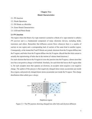
  • 1. 1 Chapter Two Diode Characteristics 2.1. PN Junction 2.2. Diode Operations 2.3. PN Diode as a Rectifier 2.4. Zener Diode Characteristics 2.5. LED and Photo Diode 2.1 PN Junction The region where the block of p- type material is joined to a block of n- type material is called a PN junction and is a fundamental component of many electronic devices, including diode, transistors and others. Remember that diffusion current flows whenever there is a surplus of carriers in one region and a corresponding lack of carriers of the same kind in another region. Consequently, at the instant the P and N blocks are joined, electrons from the N region diffuse into the P region, and holes from the P region diffuse into the N region. (Recall that this hole current is actually the repositioning of holes due to the motion of valence band electrons.) For each electron that leaves the N region to cross the junction into the P region, a donor atom that now has a net positive charge is left behind. Similarly, for each hole that leaves the P region (that is, for each acceptor atom that captures an electron), an acceptor atom acquires a net negative charge. The upshot of this process is that negatively charged donor atoms accumulate just inside the p region, and positively charged donor atoms accumulate just inside the N region. This charge distribution often called space charge. Depletion region Figure 2.1: The PN junction showing charged ions after hole and electron diffusion Δ’ P N Hole Electron
  • 2. 2 It is well known that accumulation of electric charge of opposite polarities in two separated regions cause an electric field to be established between those regions. The accumulation of positive ions in N material and negative ions in the P material established an electric field across a PN junction. The direction of field is from the positive N region to the negative P region. Figure 2.1 illustrates the field Δ’ developed across a PN junction. The accumulation of negative charge in the p region prevents additional negative charge from entering that region (like charges repel each other) and, similarly, the positively charged N region repels additional positive charge. Therefore, after the initial surge of charge across the junction, the diffusion current dwindles (becoming gradually less) to a negligible amount. The direction of electric field across the PN junction enables the flow of drift current from the P to the N region, that is, the flow of electrons from left to right and of holes from right to left, in figure 2.1. There is therefore a small drift of minority carriers in opposite direction from the diffusion current. When equilibrium condition has been established, the small reverse drift current exactly cancels the diffusion current from N to P. the net current across the junction is therefore zero. Remember that the P-region holes have been annihilated by electrons, and the N-region electrons have migrated to the P side. Because all charge carriers have been depleted (removed) from this region, it is called the depletion region. It is also called barrier region because the electric field their acts as a barrier to further diffusion current. The values of barrier potential, VO, depends on the doping levels in the P and N regions, the type of material (Si and Ge), and the temperature. VO = 𝐾𝑇 π‘ž ln 𝑁𝐴 𝑁𝐷 𝑛𝑖2 (2.1) Where, VO = barrier potential, K = Boltzmann’s constant = 1.38 Γ— 10βˆ’23 J/0 k, T = temperature of the material in Kelvin (0 k = 273 + 0 c), q = electron charge = 1.6 Γ— 10βˆ’19 c NA = acceptor doping density in the P material, ND = donor doping density in the N material
  • 3. 3 𝑛𝑖 = intrinsic electron density. VT = KT q (2.2) Where, VT = thermal voltage 2.1.1 Forward – biased junction When an external dc source is connected across a PN junction, the polarity of the connection can be such that it either opposes or reinforces the barrier. Suppose a voltage source VD is connected as shown in figure-2.2, with its positive terminal attached to the P side of a PN junction and its negative terminal attached to the N side. With polarity of connections shown in the figure 2.2, the external source creates an electric field component across the junction whose direction opposes the internal field established by the space charge. In other words, the barrier is reduced, so diffusion current is enhanced. Therefore, current flows with relative ease through the junction, its direction of flow is from P to N, as shown in figure 2.2. In this case the junction is said to be forward biased. h = hole; Δ“ = electron Figure 2.2: Forward-biased p-n junction, Narrow depletion width When the PN junction is forward biased, electrons are forced into the N region by the external source and holes are forced into the P region. As free electrons move toward the junction through the N material, a corresponding number of holes progresses through the P material. Thus, current in each region is the result of majority carrier flow. Electrons diffuse through the depletion region and recombine with holes in the P material. For each hole that recombines with an electron, an electron from a covalent bond leaves the P region and enters the positive terminal of the external source, thus maintaining the equality of current entering and leaving the source. Since there is a reduction in the electric field barrier at the forward- biased junction, there is a corresponding Δ’ h Δ“
  • 4. 4 reduction in the quantity of ionized acceptor and donor atoms required to maintain the field. As a result, the depletion region narrows under forward bias. 2.1.2 Reverse - biased junction When the positive terminal of the source is connected to the N side of the junction and the negative terminal is connected to the P side (shown in figure 2.3) the polarity of the bias voltage reinforces, or strengthens, the internal barrier field at the junction. Consequently, diffusion current is inhibited to an even greater extent than it was with no bias applied. The increased field intensity must be supported by an increase in the number of ionized donor and acceptor atoms, so the depletion regions widen under reverse bias. Figure 2.3: Reverse - biased p-n junction, wide depletion region Recall that, the unbiased PN junction has a component of drift current consisting of minority carriers that cross the junction from the P to the N side. This reverse current is the direct result of the electric field across the depletion region. Since a reverse – biasing voltage increases the magnitude of that field, we can expect the reverse current to increases correspondingly. The current magnitude is very much smaller than the current that flows under forward bias. The distinction between the ways a PN junction reacts to a bias voltage, very little current flow when it is reverse biased and substantial current flow when it is forward biased, makes it very useful device in many circuit applications. 2.2 Diode operation Diode is made up of a small piece of semiconductor material, usually silicon, in which half is doped as a p region and half is doped as an n region with a pn junction and depletion region in between. The p region is called the anode and is connected to a conductive terminal. The n region
  • 5. 5 is called the cathode and is connected to a second conductive terminal. The basic diode structure and schematic symbol are shown in Figure 2–4 given below. Figure 2.4 schematic symbol of diode. 2.2.1 Characteristics of ideal & practical diode Understanding the operation of the semiconductor diode is the basis for an understanding of all semiconductor devices. It is the simplest of semiconductor devices but plays a very vital role in electronic systems, having characteristics that closely match those of a simple switch. The term ideal refers to any device or system that has ideal characteristics perfect in every way. The ideal diode is a two-terminal device having the symbol and characteristics shown in figure 2.5, a and b respectively. The characteristics of an ideal diode are those of a switch that can conduct current in only one direction. Figure 2.5 Conduction (a) and non-conduction (b) state of Ideal diode The P side of the diode is called its anode and the N side is called its cathode. ID = IS (𝑒 𝑉𝐷 πœ‚π‘‰π‘‡ βˆ’ 1) (2.3) ID = current; VD = voltage (positive for forward bias and negative for reverse bias). IS = saturation current; Ξ· = emission coefficient; VT = thermal voltage.
  • 6. 6 Figure 2.6: I-V relations in a PN junction under forward and reverse bias 1) A silicon diode has a reverse saturation current of 7.12nA at room temperature of 27oc. Calculate its forward current if it is forward biased with a voltage of 0.7v. Solution: The given values are Is = 7.2nA, K=1.38*10e-23 J/K, Q = 1.6*10-19 C V = + 0.7 v as forward biased. πœ‚ = 2 for silicon diode T = 270 𝐢 = 27 + 273 = 3000 𝐾 Now VT = KT/q = 8.62 x 10-5 x 300 = 0.026 v Using diode current equation, I = 4.99 x 10⁻³A = 5mA. Thus, the forward current is 5mA. I) The Ideal Diode Model The ideal model of a diode is the least accurate approximation and can be represented by a simple switch as shown in the figure 2.7 below. Figure 2.7 V-I characteristics of ideals diodes
  • 7. 7 When the diode is forward-biased, it ideally acts like a closed (on) switch, as shown in Figure 2.7 (a). When the diode is reverse-biased, it ideally acts like an open (off) switch, as shown in part (b). In Figure 2.7 (c), the ideal V-I characteristic curve graphically depicts the ideal diode operation. II) The Practical Diode Model The practical model includes the barrier potential. When the diode is forward-biased, it is equivalent to a closed switch in series with a small equivalent voltage source (VF) equal to the barrier potential (0.7 V) with the positive side toward the anode, as indicated in Figure 2.8 (a). This equivalent voltage source represents the barrier potential that must be exceeded by the bias voltage before the diode will conduct and is not an active source of voltage. When conducting, a voltage drop of 0.7 V appears across the diode. When the diode is reverse-biased, it is equivalent to an open switch just as in the ideal model, as shown in Figure 2.8 (b). The barrier potential does not affect reverse bias, so it is not a factor. The characteristic curve for the practical diode model is shown in Figure 2.8 (c). Figure 2.8 V-I characteristics of practical diodes 2.2.2 Breakdown The reverse current also deviates from that predicted by the ideal diode equation if the reverse biasing voltage is allowed to approach a certain value called the reverse break down voltage, VBR. A very small increase in reverse bias voltage in the vicinity of VBR results in a very large increase in reverse current. In other word the diode no longer exhibits its normal characteristics of maintaining a very small, essentially constant reverse current with increasing reverse voltage.
  • 8. 8 Figure 2.9: a plot of the I-V relation for diode, showing the sudden increase in reverse current near the reverse break down voltage. In ordinary diodes, the breakdown phenomenon occurs because the high electric field in the depletion region impart high kinetic energy (large velocities) to the carriers crossing the region, and when these carriers collide with other atoms, they rupture covalent bonds. The large numbers of carriers that are freed in this way accounts for the increase in reverse current through the junction. The process is called avalanching. The magnitude of the reverse current that flows when V approaches VBR can be predicted from the relation: I = IS 1βˆ’[ 𝑉 𝑉𝐡𝑅 ]𝑛 (2.4) Where n is a constant determined by experiment and has a value between 2 and 6. The value of the breakdown voltage depends on doping and other physical characteristics that are controlled in manufacturing. Ordinary diodes may have breakdown voltage ranging from 10 or 20 to hundreds of volts. 2.3 Diode as a Rectifier Almost all electronics circuits require a dc source of power. For portable low power systems batteries may be used. More frequently electronic equipment is energized by a power supply, a piece of equipment which converts the alternating waveform from the power lines into an essential direct voltage. A device, such as the semiconductor diode, which is capable of converting a sinusoidal input waveform (whose average value is zero) into a unidirectional waveform, with a nonzero average component, is called a rectifier. The process of converting AC to DC waveform is called rectifications. There are two types of rectifications process: 2.3.1 Half-wave rectification In half-wave rectification either the positive or negative half of the ac wave is passed, while the other half is blocked. The basic circuit for half – wave rectification is shown in figure 2.10.
  • 9. 9 Figure 2.10: Half-wave rectifier Over one full cycle, defined by the period T of figure 2.10, the average value (the algebraic sum of the areas above and below the axis) of vi is zero. During the interval t = 0 β†’ T/2 in figure 2.10 the polarity of the applied voltage vi is such as to establish β€œpressure” in the direction indicated and turn on the diode with the polarity appearing above the diode. Substituting the short-circuit equivalence for the ideal diode will result in the equivalent circuit of figure 2.11, where it is fairly obvious that the output signal is an exact replica of the applied signal. The two terminals defining the output voltage are connected directly to the applied signal via the short-circuit equivalence of the diode. Figure 2.11: Conduction region (0β†’ T/2) For the period T/2 β†’ T, the polarity of the input vi is as shown in figure 2.12 and the resulting polarity across the ideal diode produces an β€œoff” state with an open-circuit equivalent. The result is the absence of a path for charge to flow and vo = iR = (0) *R = 0 V for the period T/2 β†’ T. The input vi and the output vo were sketched together in figure 2.13 for comparison purposes.
  • 10. 10 Figure 2.12: Non-conduction region The output signal vo now has a net positive area above the axis over a full period and an average value determined by: Vdc = 0.318𝑉 π‘š (2.5) Figure 2.13: Half-wave rectified signal Note that the net effect of half – wave circuit is the conversion of an ac voltage into a (pulsating) dc voltage. The effect of using a silicon diode with VT = 0.7 V is demonstrated in figure 2.14 for the forward- bias region. The applied signal must now be at least 0.7 V before the diode can turn β€œon.” For levels of vi less than 0.7 V, the diode is still in an open-circuit state and vo = 0 V as shown in the same figure. When conducting, the difference between vo and vi is a fixed level of VT = 0.7 V and vo = vi βˆ’ VT, as shown in the figure 2.14. The net effect is a reduction in area above the axis, which naturally reduces the resulting dc voltage level. Figure 2.14: Effect of VT on Half-wave rectified signal
  • 11. 11 For situations where Vm ≫ VT, the average value is determined by Eq.2.6. 𝑉𝑑𝑐 β‰… 0.318(𝑉 π‘š βˆ’ 𝑉𝑇 ) (2.6) The peak inverse voltage (PIV) [or PRV (peak reverse voltage)] rating of the diode is the voltage rating that must not be exceeded in the reverse-bias region or the diode will enter the Zener avalanche region. The required PIV rating for the half-wave rectifier can be determined in Eq.2.7. π‘ƒπΌπ‘‰π‘Ÿπ‘Žπ‘‘π‘–π‘›π‘” β‰₯ 𝑉 π‘š (2.7) 2.3.2 Full - wave rectification A full – wave rectifier effectively inverts the negative half – pulses of a sine wave to produce an output that is a sequence of positive half – pulses with no intervals between them. It is more efficient than the half – wave rectifier. The dc level (average value) obtained from a sinusoidal input can be improved 100% using a process called full – wave rectification. Bridge network: it is the most familiar network for performing a full – wave rectification. It is shown in figure 2.15 with its four diodes in a bridge configuration. Figure 2.15: Full – wave bridge rectifier During the period t = 0 to T/2 the polarity of the input is as shown in figure 2.16a. The resulting polarities across the ideal diodes are also shown in figure 2.16a to reveal that D2 and D3 are conducting while D1 and D4 are in the β€œoff” state. The net result is the configuration of figure 2.16b, with its indicated current and polarity across R. Since the diodes are ideal the load voltage is vo = vi, as shown in the same figure.
  • 12. 12 Figure 2.16: (a) Network of figure 2.15 for the period 0 β†’T/2 of the input voltage vi. (b) Conduction path for the positive region of vi For the negative region of the input the conducting diodes are D1 and D4, resulting in the configuration of figure 2.17. The important result is that the polarity across the load resistor R is the same as in figure 2.16a, establishing a second positive pulse, as shown in figure 2.17. Figure 2.17: Conduction path for the negative region of vi Over one full cycle the input and output voltages will appear as shown in figure 2.18. Since the area above the axis for one full cycle is now twice that obtained for a half-wave system, the dc level has also been doubled. 𝑉𝑑𝑐 = 0.636𝑉 π‘š (2.8) Figure 2.18: input and output waveform for a full-wave rectifier If silicon rather than ideal diodes is employed as shown in figure 2.19, an application of Kirchhoff’s voltage law around the conduction path would result in 𝑣𝑖 βˆ’ 𝑉𝑇 βˆ’ π‘£π‘œ βˆ’ 𝑉𝑇 = 0
  • 13. 13 π‘£π‘œ = 𝑣𝑖 βˆ’ 2𝑉𝑇 The peak value of the output voltage vo is therefore 𝑉 π‘œπ‘šπ‘Žπ‘₯ = 𝑉 π‘š βˆ’ 2𝑉𝑇 For situation where Vm≫ 2VT the average value is determined by Eq.2.9 𝑉𝑑𝑐 β‰… 0.636 (𝑉 π‘š βˆ’2𝑉𝑇) (2.9) Figure 2.19: Determining 𝑉 π‘œπ‘šπ‘Žπ‘₯ for silicon diodes in the bridge configuration 𝑃𝐼𝑉 π‘“π‘’π‘™π‘™βˆ’π‘€π‘Žπ‘£π‘’ π‘π‘Ÿπ‘–π‘‘π‘”π‘’ π‘Ÿπ‘’π‘π‘‘π‘–π‘“π‘–π‘’π‘Ÿ β‰₯ 𝑉 π‘š (2.10) 2.4 Zener diode Zener diode is a reverse-biased heavily doped p-n junction diode which is operated in the breakdown region. The symbol of a Zener diode is shown in figure 2.20a. It is like an ordinary p- n junction diode except that it is properly doped so as to have a sharp breakdown voltage. When forward biased, its characteristics are similar to that of an ordinary diode. It is always reverse biased and has sharp breakdown voltage, called the Zener voltage. By controlling the junction width and doping densities of diode it is possible to make it to breakdown at a sharp specified Zener voltage from about 2 to 200 V. A Zener diode is specified by its breakdown voltage and the maximum power dissipation. Figure 2.20: (a) Zener diode, (b) the normal operation region of Zener diode is shaded
  • 14. 14 The most common application of a Zener diode is the voltage stabilization. The Zener diode in breakdown maintains an almost constant voltage across itself over a wide current range. The complete equivalent circuit of the Zener diode in the Zener region includes a small dynamic resistance and dc battery equal to the Zener potential, as shown in figure 2.21. For all applications to follow, however, we shall assume as a first approximation that the external resistors are much larger in magnitude than the Zener-equivalent resistor and that the equivalent circuit is simply the one indicated in figure 2.21b. Figure 2.21: Zener equivalent circuit (a) complete (b) approximate Zener diodes are most frequently used in regulator networks or as a reference voltage. 2.5 LED, LCD and Photo Diode 2.5.1 Light - Emitting Diodes The increasing use of digital displays in calculators, watches, and all forms of instrumentation has contributed to the current extensive interest in structures that will emit light when properly biased. The two types in common use today to perform this function are the light-emitting diode (LED) and the liquid-crystal display (LCD). As the name implies, the light-emitting diode (LED) is a diode that will give off visible light when it is energized. In any forward-biased p-n junction there is, within the structure and primarily close to the junction, a recombination of holes and electrons. This recombination requires that the energy possessed by the unbound free electron be transferred to another state. In all semiconductor p-n junctions some of this energy will be given off as heat and some in the form of photons. In silicon and germanium, the greater percentage is given up in the form of heat and the emitted light is insignificant. In other materials, such as gallium arsenide phosphide (GaAsP) or gallium phosphide (GaP), the number of photons of light energy emitted is sufficient
  • 15. 15 to create a very visible light source. The process of giving off light by applying an electrical source of energy is called electroluminescence. As shown in figure below with its graphic symbol, the conducting surface connected to the p- material is much smaller, to permit the emergence of the maximum number of photons of light energy. Note in the figure that the recombination of the injected carriers due to the forward-biased junction results in emitted light at the site of recombination. There may, of course, be some absorption of the packages of photon energy in the structure itself, but a very large percentage are able to leave, as shown in figure. Figure 2.22: (a) Process of electroluminescence in the LED; (b) graphic symbol 2.5.2 Photodiodes While LEDs emit light, Photodiodes are sensitive to received light. They are constructed so their p-n junction can be exposed to the outside through a clear window or lens. In Photoconductive mode the saturation current increases in proportion to the intensity of the received light. This type of diode is used in CD players. In Photovoltaic mode, when the p-n junction is exposed to a certain wavelength of light, the diode generates voltage and can be used as an energy source. This type of diode is used in the production of solar power. Figure 2.23: Schematic symbols for photodiodes