
Recommended
More Related Content
What's hot
What's hot (20)
Similar to Semiconductor Diode Basics
Similar to Semiconductor Diode Basics (20)
More from HarshitParkar6677
More from HarshitParkar6677 (20)
Recently uploaded
Recently uploaded (20)
Semiconductor Diode Basics
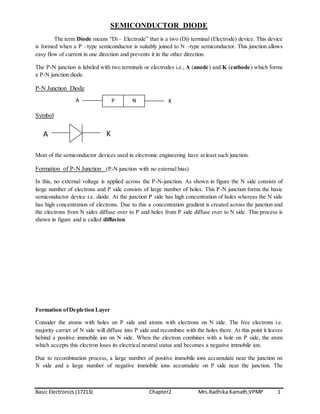
- 1. Basic Electronics (17213) Chapter2 Mrs.Radhika Kamath,VPMP 1 SEMICONDUCTOR DIODE The term Diode means “Di – Electrode” that is a two (Di) terminal (Electrode) device. This device is formed when a P –type semiconductor is suitably joined to N –type semiconductor. This junction allows easy flow of current in one direction and prevents it in the other direction. The P-N junction is labeled with two terminals or electrodes i.e., A (anode) and K (cathode) which forms a P-N junction diode. P-N Junction Diode Symbol Most of the semiconductor devices used in electronic engineering have at least such junction. Formation of P-N Junction (P-N junction with no external bias) In this, no external voltage is applied across the P-N-junction. As shown in figure the N side consists of large number of electrons and P side consists of large number of holes. This P-N junction forms the basic semiconductor device i.e. diode. At the junction P side has high concentration of holes whereas the N side has high concentration of electrons. Due to this a concentration gradient is created across the junction and the electrons from N sides diffuse over to P and holes from P side diffuse over to N side. This process is shown in figure and is called diffusion. Formation ofDepletion Layer Consider the atoms with holes on P side and atoms with electrons on N side. The free electrons i.e. majority carrier of N side will diffuse into P side and recombine with the holes there. At this point it leaves behind a positive immobile ion on N side. When the electron combines with a hole on P side, the atom which accepts this electron loses its electrical neutral status and becomes a negative immobile ion. Due to recombination process, a large number of positive immobile ions accumulate near the junction on N side and a large number of negative immobile ions accumulate on P side near the junction. The A K P NA K
- 2. Basic Electronics (17213) Chapter2 Mrs.Radhika Kamath,VPMP 2 negatively charged ions in P-side start repelling the electrons which attempt to diffuse on P-side and thus further diffusion totally stops. Thus, a region has only immobile icons and no free charge carriers like holes or electrons. This region which is “depleted” of the free charge carriers is called depletion region or space charge region. The width of this region is very small of the order of 0.5 to 1 micron, (1 micron = 1 X 10⁻⁶ meter) as compared to the widths of P and N regions. Barrier Potential or Junction Potential: The immobile positive and negative ions on the opposite sides of the PN junction develops an electric field across the junction. This electric field is called the Barrier Potential or Junction Potential.This is also termed as cut-in voltage. The junction potential for silicon is 0.7 V and for germanium it is 0.3V. The barrier potential does not allow the electrons and holes to cross the junction. To overcome this we have to apply external voltage of appropriate polarity. The moment the external voltage is greater than junction potential or cut- in voltage, the electrons and holes can holes can travel across the junction. External Biasing ofP-N junction Applying external voltage to the P-N junction is called external biasing. This voltage can be applied in two ways: i. Forward Bias ii. Reverse Bias I. Forward Biasing ofa P-N junction diode When a positive terminal of external DC supply voltage is connected to P region (anode) of diode and a negative terminal is connected to N region (cathode) of diode, then it is a forward biasing condition as shown in figure. Due to forward biased condition, free electrons from N-side are pushed towards P side holes from P side are pushed towards N side. This effectively reduces the width of the depletion region and
- 3. Basic Electronics (17213) Chapter2 Mrs.Radhika Kamath,VPMP 3 thus barrier potential is reduced. The diode is in ON state. The moment applied to voltage increases above barrier potential or cut-in voltage and a heavy current starts flowing through the diode as shown in figure. II. Reverse Biasing of PN junction Diode When a positive terminal of external DC power supply, is connected to N region (cathode) of a diode and negative terminal is connected to P region (anode) of a diode then it is reverse biasing condition of diode as shown in figure. Due to voltage applies in the polarities shown in figure the electrons and holes move away from the junction and the width of depletion region increases and diode is in OFF state, as there is no current flowing across the junction due to the majority carriers. But there is a small amount (µA) of current flowing in reverse direction due to the minority carriers i.e. holes in N region and electrons in P region. This reverse current is dependent upon the temperature. If the reverse voltage is increased beyond reverse current flows through the diode and diode is permanently damaged.
- 4. Basic Electronics (17213) Chapter2 Mrs.Radhika Kamath,VPMP 4 Experimental set up for V-I Characteristics ofa P-N Junction Diode As shown in figure the set up comprises of voltmeter connected across the diode and ammeter connected in series to measure voltage and current values. The V-I characteristics of a diode are studied under three conditions: 1. Zero external voltage: - In figure when the switch is open, the potential barrier at the PN junction will not permit the current flow. Hence the circuit current is zero as indicated by point O is characteristics of figure. 2. Forward bias: - When the switch in figure positive supply terminal is applied to P regions (anode) and negative to N region cathode under this condition, the diode is forward biased. Then applied voltage exceeds the cut in voltage(0.3V for Ge or 0.6V for Si) a heavy anode current starts flowing across. The junction which is shown in figure. Once the diode is in conduction, there is a steady voltage drop of 0.7V across it and the anode current goes on increasing according to the applied voltage. 3. Reverse bias:- in the set up of figure is we interchange the polarity of DC supply then negative terminal will be connected to P region (anode) and positive or N region (cathode). Under such conditions the depletion width will increase and junction resistance becomes very high. Practically no current flows through the junction except the reverse saturation current due to minority charge carriers. If reverse voltage is increases steadily, the kinetic energy of electrons (minority carriers) may become high to knock out the electrons from atoms. Here the junction breakdown occurs. There is a sudden increase in reverse current as shown in figure of V-I characteristics. This may destroy the P-N junction permanently. Hence,it is advised not to apply reverse breakdown voltage.
- 5. Basic Electronics (17213) Chapter2 Mrs.Radhika Kamath,VPMP 5 Ideal Diode: In Ideal condition, the diode acts as a perfect conductor when forward biased and as a perfect insulator when reverse biased. The VI characteristics of such an ideal diode is as shown below. An ideal diode acts like an automatic switch. The switch is closed when the diode is forward biased and is open when it is reverse biased. Also, ideal diode is a device which conducts with zero resistance when forward biased and appears as infinite resistance when reverse biased. Comparison ofSi and Ge Diode Parameter Si diode Ge diode 1 Material used Silicon Germanium 2 Cut in voltage 0.7V 0.3V 3 Breakdown voltage Higher Lower 4 Reverse saturation current In nA In µA 5 Temperature range 200o C 100o C 6 Applications Rectifier, clippers, clampers, Signal conditioning circuits etc. Low voltage and low temperature applications. 7 Peak Inverse Voltage 1000V 400V Important Definitions Knee voltage It is the forward voltage at which, the forward current through junction starts increasing rapidly. It is also termed as cut-in voltage. Its value is 0.7V for silicon diode and 0.3V for germanium diode. Static Resistance A DC current flows through the diode when a DC voltage is applied. The operating point on characteristic curve of diode does not change its position with time. The resistance of diode at operating point is obtained by taking ration of VF to IF. This resistance offered by diode to the forward biased DC operating conditions is called static resistance or DC resistance. AC or Dynamic Resistance (Rf) When AC voltage is applied to a diode, the operating point does not remain fixed. Its position will keep on changing continuously due to the change in input voltage as shown in figure. In that case,dynamic forward resistance is defined as:
- 6. Basic Electronics (17213) Chapter2 Mrs.Radhika Kamath,VPMP 6 Dynamic resistance RF = ΔVF/ΔIF Breakdown Voltage It is the minimum reverse voltage at which P-N junction breaks down with a sudden rise in the reverse current. PIV (Peak Inverse Voltage) :It is the maximum voltage that can be applied to the diode without damaging it. Maximum forward voltage: It is the maximum forward voltage that the diode can withstand without burnout. Power dissipation:Maximum power that the diode can safely dissipate on a continuous basis. Zener Diode A Zener diode is a special type of properly doped crystal diode which is designed to operate in the reverse breakdown region. A Zener diode is heavily doped to reduce the reverse breakdown voltage compared to ordinary P-N junction diode. Thus, the width of depletion layer of Zener diode is very less. Symbol and working principle of Zener Diode As shown in figure Zener diode symbol with two terminals anode (A) and cathode (K) is drawn. As shown in figure, when a reverse bias on Zener diode is increases, at a critical voltage called Zener breakdown voltage, the reverse current increases sharply to high value and a sudden increase in current is observed. (A satisfactory explanation of this phenomenon was first given by the scientist C-Zener. Hence, this special diode is named after him.) Figure shows the V-I characteristics of Zener diode and the Zener breakdown voltage Vz in the reverse biased region. VI Characteristics ofZener Diode:
- 7. Basic Electronics (17213) Chapter2 Mrs.Radhika Kamath,VPMP 7 Forward Biasing ofZener Diode When anode is connected to positive terminal and cathode to a negative terminal of a battery, the Zener diode is forward biased. In this mode, it works similar to a P-N junction diode as shown in above fig. The zener diode is normally not used in forward biased condition. Reverse Biasing ofZener Diode When anode is connected to a negative terminal and cathode is connected to positive terminal of a battery, the Zener diode is reverse biased. At knee or Zener breakdown voltage, a heavy reverse current also called as Zener current (Iz) starts flowing through the Zener. This point onwards the voltage across and the Zener remains constant and hence, Zener can be used as a voltage regulator in this region. The breakdown voltage depends on the amount of doping. If diode is heavily doped, then breakdown voltage is low. If diode is lightly doped, then the breakdown occurs at high voltage. Salient Features ofZener Diode i. Always operated in reverse biased fashion. ii. Zener breakdown voltage is proportional to the amount of doping. iii. In a circuit, always operate with one current limiting resister. iv. In forward biased conditions, it shows characteristics similar to P-N junction diode. Application Zener diode as Voltage Regulator i. In protection circuits for MOSFET ii. In clipping circuits iii. In pulse amplifier iv. In regulated power supplies Zener diode as Voltage Regulator A reverse biased Zener diode is used to provide a constant voltage across the load resister RL. Breakdown Mechanisms in Zener Diode Two different mechanisms of breakdown are observed in Zener diode: i. Zener Breakdown ii. Avalanche Breakdown 1. Zener Breakdown This breakdown is observed in Zener diodes having VE less than 5 V or between 5 to 8 V. When a reverse voltage for such Zener is applied, it imposes a very intense electric field across a narrow depletion width of the zener diode. The field intensity is approx. 3 X 10⁵ V/cm. This ruptures the covalent bonds and valence electrons are pulled into conduction band. These free electrons now can constitute a large reverse current at the Zener breakdown voltage. This effect is called “Zener Breakdown”. At this point, the diode from excessive heating. This breakdown voltage decreases further if there is increase in junction temperature. 2. Avalanche breakdown This breakdown is observed in the Zener diodes having VZ greater than 8 V. When a reverse voltage is applied, the conduction takes place due to the minority carriers. With increase reverse bias, these minority carriers acquire more kinetic energy and they collide with the stationary
- 8. Basic Electronics (17213) Chapter2 Mrs.Radhika Kamath,VPMP 8 atoms. During this process, they break covalent bonds to make the valence electrons jump into the conduction band for free conduction. The newly generated electrons again get accelerated to knock out more valence electrons with further collisions. This cumulative process is called “carrier multiplication”. Thus in a very short time, a large reverse current starts flowing through the Zener diode and the breakdown thus occurred is called “Avalanche Breakdown” or a “Avalanche Effect” a current limiting resistor, in series with Zener diode, avoids the damage due to excessive heating. The avalanche breakdown voltage increases with increase in junction temperature. Difference between Zener Breakdown and Avalanche Breakdown Zener Breakdown Avalanche Breakdown 1 Observed in the Zener diodes having VZ between 5 to 8 V. Observed in the Zener diodes having VZ greater than 8 V. 2 The Zener breakdown is very sharp. The avalanche breakdown shows gradual change. 3 Due to very intense field across the narrow depletion region, the valence electrons are pulled into conduction band in this breakdown. Due to collision of accelerated minority carriers, the valence electrons are pushed into conduction band. 4 The breakdown voltage decreases with increase in temperature. The breakdown voltage increases with increase in temperature.