CSL Seminar presented by Cassiano Campes - 17-07-05
•
1 like•268 views

This is the Seminar presentation performed during the CSL seminar on July 5th, 2017. The referred paper is the following: Cai, Yu, et al. "Vulnerabilities in MLC NAND flash memory programming: experimental analysis, exploits, and mitigation techniques." High Performance Computer Architecture (HPCA), 2017 IEEE International Symposium on. IEEE, 2017.

Recommended
Recommended
More Related Content
Similar to CSL Seminar presented by Cassiano Campes - 17-07-05
Similar to CSL Seminar presented by Cassiano Campes - 17-07-05 (20)
More from Cassiano Campes
Recently uploaded
Recently uploaded (20)
CSL Seminar presented by Cassiano Campes - 17-07-05
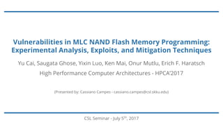
- 1. Vulnerabilities in MLC NAND Flash Memory Programming: Experimental Analysis, Exploits, and Mitigation Techniques CSL Seminar - July 5th , 2017 Yu Cai, Saugata Ghose, Yixin Luo, Ken Mai, Onur Mutlu, Erich F. Haratsch High Performance Computer Architectures - HPCA’2017 (Presented by: Cassiano Campes - cassiano.campes@csl.skku.edu)
- 2. Introduction: NAND Flash Technology 2Computer Systems Laboratory
- 3. How data is Stored in NAND Flash 3 ■ Data is represented through voltage thresholds ■ Floating gate stores the voltage level Computer Systems Laboratory ■ Greatly reduced per-bit costs by storing multiple bits per cell ■ MLC, TLC, QLC technologies
- 4. Voltage Thresholds in a NAND Flash 4 ■ Data is represented by using different voltage thresholds Computer Systems Laboratory
- 5. Read Operation: 2-bits MLC 5Computer Systems Laboratory ■ Data depends on the threshold voltage inside FG
- 6. Read Operation: 2-bits MLC 6Computer Systems Laboratory ■ Data depends on the threshold voltage inside FG
- 7. Read Operation: 2-bits MLC 7Computer Systems Laboratory ■ Reading the MSB page from a flash cell Voltage references
- 8. Read Operation: 2-bits MLC 8Computer Systems Laboratory ■ Reading the MSB page from a flash cell Voltage references
- 9. Read Operation: 2-bits MLC 9Computer Systems Laboratory ■ Reading the LSB page from a flash cell Voltage references
- 10. Read Operation: 2-bits MLC 10Computer Systems Laboratory ■ Reading the LSB page from a flash cell Voltage references
- 11. Write States of a Flash Cell 11Computer Systems Laboratory
- 12. Write States of a Flash Cell 12Computer Systems Laboratory Erased as 11
- 13. Write States of a Flash Cell 13Computer Systems Laboratory *ISPP: incremental step pulse programming
- 14. Write States of a Flash Cell 14Computer Systems Laboratory ISPP write *ISPP: incremental step pulse programming
- 15. Write States of a Flash Celll 15Computer Systems Laboratory ΔVth
- 16. Write States of a Flash Cell 16Computer Systems Laboratory Check state
- 17. Write States of a Flash Cell 17Computer Systems Laboratory
- 18. Write States of a Flash Cell 18Computer Systems Laboratory ISPP write *ISPP: incremental step pulse programming
- 19. Write States of a Flash Cell 19Computer Systems Laboratory ΔVth ΔVth
- 20. Cell-to-cell Program Interference 20Computer Systems Laboratory ■ Threshold voltage of a neighboring cell may increase ■ Worsens as flash memory scales (1X nm) ■ Mitigation: two-step programming ■ LSB programming ■ MSB programming
- 21. Shadow Program Sequencing 21Computer Systems Laboratory ■ Each page within a block is assigned a unique page number ■ LSB: 2i -1 ■ MSB: 2i + 2
- 22. Shadow Program Sequencing 22Computer Systems Laboratory
- 23. Shadow Program Sequencing 23Computer Systems Laboratory
- 24. Shadow Program Sequencing 24Computer Systems Laboratory
- 25. Shadow Program Sequencing 25Computer Systems Laboratory
- 26. Shadow Program Sequencing 26Computer Systems Laboratory
- 27. Shadow Program Sequencing 27Computer Systems Laboratory
- 28. Shadow Program Sequencing 28Computer Systems Laboratory
- 29. Shadow Program Sequencing 29Computer Systems Laboratory
- 30. Read Disturb 30Computer Systems Laboratory ■ Read to one data page can affect neighboring cells ■ Unread pages may shift its threshold voltages slightly
- 31. Error-Correction Code 31Computer Systems Laboratory ■ Provides mechanisms to correct errors in pages ■ Can correct few bit errors ■ ECC is kept in the NAND controller
- 32. Raw Bit Error Rate, ECC and Lifetime 32Computer Systems Laboratory ■ RBER are the raw bit errors before data is corrected by ECC ■ RBER occurs at any point of the NAND lifetime ■ RBER limits the total lifetime of memory ■ Naturally, as the cell wears out, more RBER occurs
- 33. Raw Bit Error Rate, ECC and Lifetime 33Computer Systems Laboratory ■ Function of ECC capacity and P/E cycles determines lifetime
- 34. Error Sources in Two-step Programming 34Computer Systems Laboratory ■ MSB depends on the LSB values to be written ■ LSB does not pass through the ECC engine (latency)
- 35. Problems: Characterization of Error Sources 35Computer Systems Laboratory
- 36. Cell-to-Cell Program Interference 36Computer Systems Laboratory ■ Interference on the LSB page is no longer negligible
- 37. Interference in the ER State 37Computer Systems Laboratory ■ RBER are the raw bit errors before data is corrected by ECC ■ RBER occurs at any point of the NAND lifetime ■ RBER limits the total lifetime of memory ■ Naturally, as the cell wears out, more RBER occurs
- 38. Read Disturb 38Computer Systems Laboratory ■ Cells with lower voltage threshold level are affected ■ Unprogrammed or partially-programmed cells are more likely to experience errors from read disturb ■ Quantify the impact of read disturb on: ■ Unprogrammed and partially-programmed cells
- 39. Read Disturb Experiments 39Computer Systems Laboratory Region A: fully programmed; Region B: partially programmed; Region C: unprogrammed
- 40. Read Disturb Experiments 40Computer Systems Laboratory Region A: fully programmed; Region B: partially programmed; Region C: unprogrammed
- 41. Vulnerabilities: Security exploit sketches 41Computer Systems Laboratory
- 42. Security Exploit Sketches 42Computer Systems Laboratory ■ Multiple applications share an SSD ■ Data from different apps stored in same physical SSD ■ SSDs maintain one open block for writes ■ Malicious application can inject errors into the files of others
- 43. Interference Based Exploit 43Computer Systems Laboratory ■ Worst-case data pattern (all 0s) cause 4.9x RBER neighboring page
- 44. Read Disturb Based Exploit 44Computer Systems Laboratory ■ Reading specific pages to disturb unprogrammed ones ■ fopen(), fread(), fflush(), fclose() repeatedly ■ Rapid Reads may be avoided by SSDs internal cache ■ However, simply read different pages to pollute cache ■ Read takes 100us -> 10K reads/second
- 45. Enhancement: Protection and Mitigation Mechanisms 45Computer Systems Laboratory
- 46. Protection and Mitigation Mechanisms 46Computer Systems Laboratory ■ Proposed three solutions for the problems studied
- 47. Buffering LSB Data in the Controller 47Computer Systems Laboratory * No more than two LSB pages need to be stored in the DRAM buffer at any given time
- 48. Adaptive LSB Read Reference Voltage 48Computer Systems Laboratory ■ Optimize the read reference voltage used in LSB ■ New threshold accounts the shifts ■ Reduces the number of RBER 32%
- 49. Multiple Pass-Through Voltages 49Computer Systems Laboratory ■ Reduce the gap between the threshold and reference
- 50. Multiple Pass-Through Voltages 50Computer Systems Laboratory ■ Improvements in lifetime compared to the RBER
- 51. Q&A! Thank you 51Computer Systems Laboratory
- 52. References 52Computer Systems Laboratory ■ Cai, Yu, et al. "Vulnerabilities in MLC NAND flash memory programming: experimental analysis, exploits, and mitigation techniques." High Performance Computer Architecture (HPCA), 2017 IEEE International Symposium on. IEEE, 2017.
- 53. Disclaimer 53Computer Systems Laboratory ■ All the contents here presented are based on the Cai’s research paper and his presentation found at: ■ https://people.inf.ethz.ch/omutlu/pub/flash-memory-programming-vulnerabilities_hpca17.pdf ■ http://www.ece.cmu.edu/~safari/pubs/flash-memory-programming-vulnerabilities_hpca17-talk.pdf ■ Thanks for the authors for this great research!