SlideShare a Scribd company logo
1 of 1
Download to read offline
CVD Growth of Single-Layer TMD films into Pre-Fabricated Substrate Structures
Brandon Davis, E. Preciado, V. Klee, A. E. Nguyen, I. Liu , D. Barroso, S. Naghibi, I. Liao, G Von Son, D. Martinez-Ta, Ludwig Bartels
University of California, Riverside
I. Motivation
Process Flow
V. Substrate Preparation: Suspended Growth
VI. Outlook
Before
Si
Metal
SiO2
MoS2
HfO2
After
X S S
G
D
Channel
a)
VII. Acknowledgements
Transport shows MoS2
photo-response. Design
for scalability using
photo lithography. Pillar
is under cut to prevent
continuous metal thin
film on the sidewall.
In collaboration with:
Volker Sorger
Mark Bockrath
Exposure
Silicon
SiO2
Photoresist
TMD
Key Spin Coat Resist
PL top off trench
DevelopmentEtch StepCVD Growth
II. Goal
Local Seeding Growth of TMD material exactly
where needed. At any orientation.
II. Substrate Preparation: Local Seeding
Nucleation of TMD Growth
Photo Mask
Photo Resist
Cr Layer
SiO2
Si
Exposure MoS CVD2Develop Cr Wet Etch
& Resist Strip
O Plasma Etch
& Cr Strip
2
IV. Substrate Preparation: Local Seeding
7 m
7 m
b)
c)
a)
2 m
(Left) Optical micrographs of a
patterned SiO2/Si substrate after
growth of MoS2 single-layer islands. Ø
= 2 μm holes through the substrate
oxide seed the formation of
crystalline-single-layer MoS2 islands.
2 m
(Left) AFM image
of the area
highlighted by a
white frame. AFM
confirms
homogeneous
single-layer
height.Grain
Boundaries
Photon Energy (eV)
300 400 500 600
Intensity(a.u.)Intensity(a.u.)
Raman Shift (cm-1
)
E1
2g A1g
a)
b)
1.4 1.6 1.8 2.0 2.2
(right) Raman and
photoluminescence
(PL) spectroscopy of
the MoS2 islands on
the sample. (left) PL
mapping shows high
homogeneity of the
film. A bright feature
Suspended
Material
at the location of the substrate hole
corresponds to suspended material.
CVD Growth
Tube Furnace
High Vacuum
TMD materials can be
grown by various CVD
methods.
Depending on the method,
the resultant material are
isolated highly-crystalline
islands randomly oriented
on a substrate (tube
furnace) or a homogenous,
substrate-scale film
(vacuum CVD).
Wafer-Scale: the ONLY Goal?
Conventional semiconductor epitaxy suggests
wafer-scale growth as the key goal of film
preparation. The 2D nature of the films,
however, may limit the utility of the this
approach
Vs.
D. E. Johnston, et al. “One-volt operation of High-Current Vertical channel Polymer
semiconductor Field-Effect Transistors” Nano let, 2012, 12(8), pp 4181-4186
2cm
2cm
Sample Clamp
The sample is created
by using a chromium
hard mask. First, a layer
of Chromium must be
deposited onto the
substrate, the pattern is
transferred. using
Photolithography and a
wet etch. A dry etch is
then performed. Finally
The sample has MoS2
grown onto them
Trench
10μm
• Photo mapping of
suspended vs non
suspended growth
• Suspended growth shows
a higher intensity PL then
the non suspended • The PL of non
suspended is
measured at 1.85 eV
when suspended.
• The PL of the
suspended is
measured at 1.82 eV
showing a difference
10 µm
Photo mapping over trench
PL over trench
1.76 1.81 1.85 1.89
0
5000
10000
15000
20000
25000
Intensity(a.u.)
Photon Energy (eV)
On Silicon
Suspended
170 340 510 680
0
500
1000
1500
2000
2500
3000
3500
Intensity(a.u.)
Raman Shift (cm-1)
Si
SiO2
Metal
MoS2
I. Suspended Growth: Preliminary Results
Pillared substrates
-600
-400
-200
0
200
400
600
-2 -1 0 1 2
Isd(pA)
Vsd (V)
light ON
50 µm
d)
ab
bc
cd
MoS2
MoSe2
No Substrate Quenching
Over Hole
MoSe2 Film grown over hole arrays. The PL
map show that the area over the center of
the hole has a higher intensity then the area
surrounding the hole.
100 μm
c)

More Related Content

Viewers also liked

Properties of Self-Aligned Short-Channel Graphene Field-Effect Transistors Ba...
Properties of Self-Aligned Short-Channel Graphene Field-Effect Transistors Ba...Properties of Self-Aligned Short-Channel Graphene Field-Effect Transistors Ba...
Properties of Self-Aligned Short-Channel Graphene Field-Effect Transistors Ba...Abidur Rahman
 
Pilar de Miguel-Política de innovación y de transferencia del CDTI
Pilar de Miguel-Política de innovación y de transferencia del CDTIPilar de Miguel-Política de innovación y de transferencia del CDTI
Pilar de Miguel-Política de innovación y de transferencia del CDTIFundación Ramón Areces
 
Francisco Guinea-Recent advances in graphene research
Francisco Guinea-Recent advances in graphene researchFrancisco Guinea-Recent advances in graphene research
Francisco Guinea-Recent advances in graphene researchFundación Ramón Areces
 
JeongSeuk_Kang_Research_Presentation_Dec2014
JeongSeuk_Kang_Research_Presentation_Dec2014JeongSeuk_Kang_Research_Presentation_Dec2014
JeongSeuk_Kang_Research_Presentation_Dec2014Louis Kang
 
rebeccapwong_SCI_poster_final
rebeccapwong_SCI_poster_finalrebeccapwong_SCI_poster_final
rebeccapwong_SCI_poster_finalRebecca Wong
 
Hexagonal Boron Nitride - Ubiquitous Layered dielectric for Two-Dimensional E...
Hexagonal Boron Nitride - Ubiquitous Layered dielectric for Two-Dimensional E...Hexagonal Boron Nitride - Ubiquitous Layered dielectric for Two-Dimensional E...
Hexagonal Boron Nitride - Ubiquitous Layered dielectric for Two-Dimensional E...Nikhil Jain
 
M. García Hernández-Graphene Flagship: an opportunity and a challenge
M. García Hernández-Graphene Flagship: an opportunity and a challengeM. García Hernández-Graphene Flagship: an opportunity and a challenge
M. García Hernández-Graphene Flagship: an opportunity and a challengeFundación Ramón Areces
 
Advance ceramics: Boron nitride nanosheets
Advance ceramics: Boron nitride nanosheetsAdvance ceramics: Boron nitride nanosheets
Advance ceramics: Boron nitride nanosheetsLuigi Mari Opeña
 
Iván Brihuega-Probing graphene physics at the atomic scale
Iván Brihuega-Probing graphene physics at the atomic scaleIván Brihuega-Probing graphene physics at the atomic scale
Iván Brihuega-Probing graphene physics at the atomic scaleFundación Ramón Areces
 
Midterm Symposium Presentation
Midterm Symposium PresentationMidterm Symposium Presentation
Midterm Symposium PresentationPaulo Fonseca
 
Two-Dimensional Layered Materials for Battery Application--Yifei Li
Two-Dimensional Layered Materials for Battery Application--Yifei LiTwo-Dimensional Layered Materials for Battery Application--Yifei Li
Two-Dimensional Layered Materials for Battery Application--Yifei LiYifei Li
 
seawater desalination using MoS2 nanopore POWER POINT
seawater desalination using MoS2 nanopore POWER POINTseawater desalination using MoS2 nanopore POWER POINT
seawater desalination using MoS2 nanopore POWER POINTprincely oriomojor
 
Luis Abreu-Haciendo camino con el profesor Segovia de Arana
Luis Abreu-Haciendo camino con el profesor Segovia de AranaLuis Abreu-Haciendo camino con el profesor Segovia de Arana
Luis Abreu-Haciendo camino con el profesor Segovia de AranaFundación Ramón Areces
 
Andrés Castellano-Gómez-Exotic 2D materials
Andrés Castellano-Gómez-Exotic 2D materialsAndrés Castellano-Gómez-Exotic 2D materials
Andrés Castellano-Gómez-Exotic 2D materialsFundación Ramón Areces
 
Graphene and hexagonal boron nitride filled epoxy nanocomposites
Graphene and hexagonal boron nitride filled epoxy nanocompositesGraphene and hexagonal boron nitride filled epoxy nanocomposites
Graphene and hexagonal boron nitride filled epoxy nanocompositesArun Yadav
 

Viewers also liked (20)

bht_Freiberg_Morshchagin
bht_Freiberg_Morshchaginbht_Freiberg_Morshchagin
bht_Freiberg_Morshchagin
 
Properties of Self-Aligned Short-Channel Graphene Field-Effect Transistors Ba...
Properties of Self-Aligned Short-Channel Graphene Field-Effect Transistors Ba...Properties of Self-Aligned Short-Channel Graphene Field-Effect Transistors Ba...
Properties of Self-Aligned Short-Channel Graphene Field-Effect Transistors Ba...
 
Pilar de Miguel-Política de innovación y de transferencia del CDTI
Pilar de Miguel-Política de innovación y de transferencia del CDTIPilar de Miguel-Política de innovación y de transferencia del CDTI
Pilar de Miguel-Política de innovación y de transferencia del CDTI
 
Francisco Guinea-Recent advances in graphene research
Francisco Guinea-Recent advances in graphene researchFrancisco Guinea-Recent advances in graphene research
Francisco Guinea-Recent advances in graphene research
 
Boron Nitride Spray II
Boron Nitride Spray IIBoron Nitride Spray II
Boron Nitride Spray II
 
JeongSeuk_Kang_Research_Presentation_Dec2014
JeongSeuk_Kang_Research_Presentation_Dec2014JeongSeuk_Kang_Research_Presentation_Dec2014
JeongSeuk_Kang_Research_Presentation_Dec2014
 
rebeccapwong_SCI_poster_final
rebeccapwong_SCI_poster_finalrebeccapwong_SCI_poster_final
rebeccapwong_SCI_poster_final
 
Hexagonal Boron Nitride - Ubiquitous Layered dielectric for Two-Dimensional E...
Hexagonal Boron Nitride - Ubiquitous Layered dielectric for Two-Dimensional E...Hexagonal Boron Nitride - Ubiquitous Layered dielectric for Two-Dimensional E...
Hexagonal Boron Nitride - Ubiquitous Layered dielectric for Two-Dimensional E...
 
M. García Hernández-Graphene Flagship: an opportunity and a challenge
M. García Hernández-Graphene Flagship: an opportunity and a challengeM. García Hernández-Graphene Flagship: an opportunity and a challenge
M. García Hernández-Graphene Flagship: an opportunity and a challenge
 
Advance ceramics: Boron nitride nanosheets
Advance ceramics: Boron nitride nanosheetsAdvance ceramics: Boron nitride nanosheets
Advance ceramics: Boron nitride nanosheets
 
Tomás Palacios-Redefining electronics
Tomás Palacios-Redefining electronicsTomás Palacios-Redefining electronics
Tomás Palacios-Redefining electronics
 
Iván Brihuega-Probing graphene physics at the atomic scale
Iván Brihuega-Probing graphene physics at the atomic scaleIván Brihuega-Probing graphene physics at the atomic scale
Iván Brihuega-Probing graphene physics at the atomic scale
 
Midterm Symposium Presentation
Midterm Symposium PresentationMidterm Symposium Presentation
Midterm Symposium Presentation
 
Final Presentation
Final PresentationFinal Presentation
Final Presentation
 
Two-Dimensional Layered Materials for Battery Application--Yifei Li
Two-Dimensional Layered Materials for Battery Application--Yifei LiTwo-Dimensional Layered Materials for Battery Application--Yifei Li
Two-Dimensional Layered Materials for Battery Application--Yifei Li
 
seawater desalination using MoS2 nanopore POWER POINT
seawater desalination using MoS2 nanopore POWER POINTseawater desalination using MoS2 nanopore POWER POINT
seawater desalination using MoS2 nanopore POWER POINT
 
Luis Abreu-Haciendo camino con el profesor Segovia de Arana
Luis Abreu-Haciendo camino con el profesor Segovia de AranaLuis Abreu-Haciendo camino con el profesor Segovia de Arana
Luis Abreu-Haciendo camino con el profesor Segovia de Arana
 
Andrés Castellano-Gómez-Exotic 2D materials
Andrés Castellano-Gómez-Exotic 2D materialsAndrés Castellano-Gómez-Exotic 2D materials
Andrés Castellano-Gómez-Exotic 2D materials
 
Graphene and hexagonal boron nitride filled epoxy nanocomposites
Graphene and hexagonal boron nitride filled epoxy nanocompositesGraphene and hexagonal boron nitride filled epoxy nanocomposites
Graphene and hexagonal boron nitride filled epoxy nanocomposites
 
bio sensoring
bio sensoringbio sensoring
bio sensoring
 

Similar to FINAL Brandons Poster AVS versionE

3 di metrology-slideshare
3 di metrology-slideshare3 di metrology-slideshare
3 di metrology-slideshareKeshab Paudel
 
MSE PhD lecture. Adv. Mater. Synthesis. Thin Films. Oct 23, 2014.
MSE PhD lecture. Adv. Mater. Synthesis. Thin Films. Oct 23, 2014.MSE PhD lecture. Adv. Mater. Synthesis. Thin Films. Oct 23, 2014.
MSE PhD lecture. Adv. Mater. Synthesis. Thin Films. Oct 23, 2014.Toru Hara
 
Mse phd lecture
Mse phd lectureMse phd lecture
Mse phd lectureToru Hara
 
EVA TEJEDOR ALONSO. Summary report
EVA TEJEDOR ALONSO. Summary reportEVA TEJEDOR ALONSO. Summary report
EVA TEJEDOR ALONSO. Summary reportEva Tejedor Alonso
 
Poster 18.3.15. FINALWOOOOOOOOOOOO
Poster 18.3.15. FINALWOOOOOOOOOOOOPoster 18.3.15. FINALWOOOOOOOOOOOO
Poster 18.3.15. FINALWOOOOOOOOOOOOChris Wilshaw
 
ETE444-lec5-micro-fabrication.pptx
ETE444-lec5-micro-fabrication.pptxETE444-lec5-micro-fabrication.pptx
ETE444-lec5-micro-fabrication.pptxmashiur
 
ETE444-lec5-micro-fabrication.pptx
ETE444-lec5-micro-fabrication.pptxETE444-lec5-micro-fabrication.pptx
ETE444-lec5-micro-fabrication.pptxmashiur
 
Characterization Studies of CdS Nanocrystalline Film Deposited on Teflon Subs...
Characterization Studies of CdS Nanocrystalline Film Deposited on Teflon Subs...Characterization Studies of CdS Nanocrystalline Film Deposited on Teflon Subs...
Characterization Studies of CdS Nanocrystalline Film Deposited on Teflon Subs...IJLT EMAS
 
Pulse laser deposition of thin film
Pulse laser deposition of thin filmPulse laser deposition of thin film
Pulse laser deposition of thin filmUOG PHYSICISTS !!!!!
 
University of Toronto Chemistry Librarians Workshop June 2012
University of Toronto Chemistry Librarians Workshop June 2012University of Toronto Chemistry Librarians Workshop June 2012
University of Toronto Chemistry Librarians Workshop June 2012Brock University
 
Dielectric Q-V Measurements using COS technique
Dielectric Q-V Measurements using COS techniqueDielectric Q-V Measurements using COS technique
Dielectric Q-V Measurements using COS techniqueMichael Shifrin
 
Preparation and Properties of Nanocrystalline Zinc Oxide Thin Films
Preparation and Properties of Nanocrystalline Zinc Oxide Thin FilmsPreparation and Properties of Nanocrystalline Zinc Oxide Thin Films
Preparation and Properties of Nanocrystalline Zinc Oxide Thin Filmsijtsrd
 
Pulse laser deposition of thin film (PLD)
Pulse laser deposition of thin film (PLD)Pulse laser deposition of thin film (PLD)
Pulse laser deposition of thin film (PLD)UOG PHYSICISTS !!!!!
 

Similar to FINAL Brandons Poster AVS versionE (20)

3 di metrology-slideshare
3 di metrology-slideshare3 di metrology-slideshare
3 di metrology-slideshare
 
03
0303
03
 
MSE PhD lecture. Adv. Mater. Synthesis. Thin Films. Oct 23, 2014.
MSE PhD lecture. Adv. Mater. Synthesis. Thin Films. Oct 23, 2014.MSE PhD lecture. Adv. Mater. Synthesis. Thin Films. Oct 23, 2014.
MSE PhD lecture. Adv. Mater. Synthesis. Thin Films. Oct 23, 2014.
 
Mse phd lecture
Mse phd lectureMse phd lecture
Mse phd lecture
 
Pvc cmos finale
Pvc cmos finale Pvc cmos finale
Pvc cmos finale
 
Nanolithography
NanolithographyNanolithography
Nanolithography
 
Thin film solar cells
Thin film solar cellsThin film solar cells
Thin film solar cells
 
EVA TEJEDOR ALONSO. Summary report
EVA TEJEDOR ALONSO. Summary reportEVA TEJEDOR ALONSO. Summary report
EVA TEJEDOR ALONSO. Summary report
 
Poster 18.3.15. FINALWOOOOOOOOOOOO
Poster 18.3.15. FINALWOOOOOOOOOOOOPoster 18.3.15. FINALWOOOOOOOOOOOO
Poster 18.3.15. FINALWOOOOOOOOOOOO
 
A0360105
A0360105A0360105
A0360105
 
ETE444-lec5-micro-fabrication.pptx
ETE444-lec5-micro-fabrication.pptxETE444-lec5-micro-fabrication.pptx
ETE444-lec5-micro-fabrication.pptx
 
ETE444-lec5-micro-fabrication.pptx
ETE444-lec5-micro-fabrication.pptxETE444-lec5-micro-fabrication.pptx
ETE444-lec5-micro-fabrication.pptx
 
Characterization Studies of CdS Nanocrystalline Film Deposited on Teflon Subs...
Characterization Studies of CdS Nanocrystalline Film Deposited on Teflon Subs...Characterization Studies of CdS Nanocrystalline Film Deposited on Teflon Subs...
Characterization Studies of CdS Nanocrystalline Film Deposited on Teflon Subs...
 
Pulse laser deposition of thin film
Pulse laser deposition of thin filmPulse laser deposition of thin film
Pulse laser deposition of thin film
 
Anusha
AnushaAnusha
Anusha
 
Preparation of thin films
Preparation of thin filmsPreparation of thin films
Preparation of thin films
 
University of Toronto Chemistry Librarians Workshop June 2012
University of Toronto Chemistry Librarians Workshop June 2012University of Toronto Chemistry Librarians Workshop June 2012
University of Toronto Chemistry Librarians Workshop June 2012
 
Dielectric Q-V Measurements using COS technique
Dielectric Q-V Measurements using COS techniqueDielectric Q-V Measurements using COS technique
Dielectric Q-V Measurements using COS technique
 
Preparation and Properties of Nanocrystalline Zinc Oxide Thin Films
Preparation and Properties of Nanocrystalline Zinc Oxide Thin FilmsPreparation and Properties of Nanocrystalline Zinc Oxide Thin Films
Preparation and Properties of Nanocrystalline Zinc Oxide Thin Films
 
Pulse laser deposition of thin film (PLD)
Pulse laser deposition of thin film (PLD)Pulse laser deposition of thin film (PLD)
Pulse laser deposition of thin film (PLD)
 

FINAL Brandons Poster AVS versionE

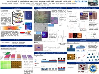
  • 1. CVD Growth of Single-Layer TMD films into Pre-Fabricated Substrate Structures Brandon Davis, E. Preciado, V. Klee, A. E. Nguyen, I. Liu , D. Barroso, S. Naghibi, I. Liao, G Von Son, D. Martinez-Ta, Ludwig Bartels University of California, Riverside I. Motivation Process Flow V. Substrate Preparation: Suspended Growth VI. Outlook Before Si Metal SiO2 MoS2 HfO2 After X S S G D Channel a) VII. Acknowledgements Transport shows MoS2 photo-response. Design for scalability using photo lithography. Pillar is under cut to prevent continuous metal thin film on the sidewall. In collaboration with: Volker Sorger Mark Bockrath Exposure Silicon SiO2 Photoresist TMD Key Spin Coat Resist PL top off trench DevelopmentEtch StepCVD Growth II. Goal Local Seeding Growth of TMD material exactly where needed. At any orientation. II. Substrate Preparation: Local Seeding Nucleation of TMD Growth Photo Mask Photo Resist Cr Layer SiO2 Si Exposure MoS CVD2Develop Cr Wet Etch & Resist Strip O Plasma Etch & Cr Strip 2 IV. Substrate Preparation: Local Seeding 7 m 7 m b) c) a) 2 m (Left) Optical micrographs of a patterned SiO2/Si substrate after growth of MoS2 single-layer islands. Ø = 2 μm holes through the substrate oxide seed the formation of crystalline-single-layer MoS2 islands. 2 m (Left) AFM image of the area highlighted by a white frame. AFM confirms homogeneous single-layer height.Grain Boundaries Photon Energy (eV) 300 400 500 600 Intensity(a.u.)Intensity(a.u.) Raman Shift (cm-1 ) E1 2g A1g a) b) 1.4 1.6 1.8 2.0 2.2 (right) Raman and photoluminescence (PL) spectroscopy of the MoS2 islands on the sample. (left) PL mapping shows high homogeneity of the film. A bright feature Suspended Material at the location of the substrate hole corresponds to suspended material. CVD Growth Tube Furnace High Vacuum TMD materials can be grown by various CVD methods. Depending on the method, the resultant material are isolated highly-crystalline islands randomly oriented on a substrate (tube furnace) or a homogenous, substrate-scale film (vacuum CVD). Wafer-Scale: the ONLY Goal? Conventional semiconductor epitaxy suggests wafer-scale growth as the key goal of film preparation. The 2D nature of the films, however, may limit the utility of the this approach Vs. D. E. Johnston, et al. “One-volt operation of High-Current Vertical channel Polymer semiconductor Field-Effect Transistors” Nano let, 2012, 12(8), pp 4181-4186 2cm 2cm Sample Clamp The sample is created by using a chromium hard mask. First, a layer of Chromium must be deposited onto the substrate, the pattern is transferred. using Photolithography and a wet etch. A dry etch is then performed. Finally The sample has MoS2 grown onto them Trench 10μm • Photo mapping of suspended vs non suspended growth • Suspended growth shows a higher intensity PL then the non suspended • The PL of non suspended is measured at 1.85 eV when suspended. • The PL of the suspended is measured at 1.82 eV showing a difference 10 µm Photo mapping over trench PL over trench 1.76 1.81 1.85 1.89 0 5000 10000 15000 20000 25000 Intensity(a.u.) Photon Energy (eV) On Silicon Suspended 170 340 510 680 0 500 1000 1500 2000 2500 3000 3500 Intensity(a.u.) Raman Shift (cm-1) Si SiO2 Metal MoS2 I. Suspended Growth: Preliminary Results Pillared substrates -600 -400 -200 0 200 400 600 -2 -1 0 1 2 Isd(pA) Vsd (V) light ON 50 µm d) ab bc cd MoS2 MoSe2 No Substrate Quenching Over Hole MoSe2 Film grown over hole arrays. The PL map show that the area over the center of the hole has a higher intensity then the area surrounding the hole. 100 μm c)