SlideShare a Scribd company logo
1 of 12
Download to read offline
Preparation of thin films By SILAR method
Washing
R.Gandhimathi
Thin - less than about one micron
Film - layer of material on surface
▪ Thin films are ( low dimensional materials)
thin material layers ranging from fractions of
a nm to several m in thickness
▪ Created by condensing, species of matter
(either by one by one atomic/molecular/ionic
deposition )
▪ Thin films, both crystalline and amorphous
▪ Thin film deposition is performed at very
low pressures high vacuum
Introduction to thin films
• Solar cells
• Light-emitting diodes
• Photoconductors
• Light crystal displays
• Magneto-optic memories
• Electro-optic coatings
• Multilayer capacitors
• Flat-panel displays
• Smart windows
• Computer chips
• Magneto-optic discs
• Lithography
• Microelectromechanical systems (MEMS)
• Multifunctional emerging coatings
Applications of thin film technology
▪ Electronic semiconductor devices and optical coatings are the main applications
benefiting from thin film construction
▪ Properties of material significantly differ when analyzed in the form of thin films
▪ Allows easy integration into various types of devices
▪ Key elements in the fields of optoelectronic, photonic, and magnetic devices
Why thin films?
Thin film deposition is the process of creating and
depositing thin film coatings onto a substrate material
To obtain thin films with good quality, there are
different deposition techniques
Thin film
deposition
techniques
Thin film deposition
• Movement of vaporized target atoms or molecules to
the substrate
• Formation of layers by atoms or molecule
• Growth of the layered atoms or molecule
Layer Island Layer + Island
(Frank vander) (Merwe Volmer-Weber) (Stranski-Krastanov)
Thin film Growth modes
Atoms strongly
bound to substrate
Atoms strongly
bound to each other
Mixture of 1 & 2
Lattice
mismatch
induces
Island
formation
Adatom: An atom intended to be adsorbed and incorporated on the surface
Physisorption: Adsorption of the arriving atoms on the deposition surface through weak
vander waals forces
Surface diffusion: Diffusion of the physisorbed species on the surface before they get
incorporated into the film
Chemisorption: Reaction of the physisorbed species with each other and the deposition
surface to form the bonds of the film material
When island clusters coalesce/
combine, eventually form a
continuous film
Nucleation and growth
▪ A vaporization coating process
▪ Material is removed from a target and deposited on to a substrate
▪ Basic mechanism : An atom-by-atom transfer of material from the
solid phase to the vapor phase and back to the solid phase, gradually
building a film on the surface to be coated
▪ Materials to be deposited are heated to the point of vaporization,
and then evaporate to form to a thin film covering the surface of the
substrate E.g., Depositing metal films. Aluminum, gold and other
metals
▪ All film deposition takes place under vacuum or very carefully
controlled atmosphere
Physical Vapor Deposition (PVD)
▪ Chemically reacted materials at the substrate surface form thin
film of product material
▪ Chemical reactions may depend on thermal effects as in vapor
phase deposition and thermal growth.
▪ A definite chemical reaction is required to obtain the final film
Chemical Vapor Deposition (CVD)
Successive ionic layer adsorption and reaction (SILAR)
▪ Adsorptions of cations on surface of substrate
▪ Washing residue of electrolytes with the solvent
▪ Adsorptions pf anions on surface of substrate
▪ Washing residue of electrolytes with the solvent
▪ Among various chemical methods, the sequential
ionic layer adsorption reaction (SILAR) has been
shown to be one that most suitable for preparing
semiconductor materials
▪ A facile, low-cost growth method for the
fabrication semiconductors solar cells
o A binary semiconductor AB, where A - cation A+ and B -
anion, then ideally the lattice should have the atomic
arrangement of ABABAB·····.
o A SILAR process can produce such an arrangement by
sequential immersion of a substrate into a cationic solution
and an anionic solution
o Process can be repeated to increase the amount of deposited
material and the size of NCs
o In a real experiment, parameters such as solution
concentration, dipping time, temperature are crucial in
obtaining the desired semiconductor quality
Applications
▪ Semiconductors
▪ Oxide of metals
▪ nanocomposites
▪ polymer inorganic nanoparticles
composites
▪ porous materials & nanoparticles
Advantages
• Excellent material utilization efficiency
• Good control over the deposition
process along with the film thickness
• Cost effective and user friendly
• Large scale deposition capability on
virtually any type of substrate
• Easy control on film thickness by
adjusting number of deposition cycles is
the beauty of this method.
Precursors: Cadmium chloride CdCl2 solution
Sodium sulphide Na2S solution
Substrate: Precleaned Glass or FTO
Deposition parameters for getting adherent
thin films
▪ Concentration of the solution
▪ pH of the reacting baths,
▪ temperature of deposition
▪ Substrate treatment
▪ Deposition time
Under optimized deposition conditions
only, adherent thin films can be produced
Preparation of Cadmium sulphide CdS thin films
• A chemical dipping technique
• Involves successive dipping of a precleaned
substrate in separately placed cationic and
anionic precursor
• Between every immersion it is rinsed in ion
exchanged water
Na2S
solution
CdCl2
⋅2H2O]
solution
Adsorption of
cationic metal ions
Washing
Adsorption of
anionic ions
Reaction on the substrate
lead to the formation of
metal sulphide ion
Washing
Cadmium sulphide -optoelectronic applications
▪ solar cells
▪ photodiodes
▪ light emitting diodes
▪ nonlinear optics
▪ heterogeneous photocatalysis
▪ high-density magnetic information storage
Precursors: Cadmium acetate Cd(CH3COO)2 ⋅2H2O] solution
Ammonium sulphide [(NH4)2S] solution (OR)
Sodium sulphide Na2S solution
Substrate: Precleaned Glass or FTO
[(NH4)2S]
solution
Cd(CH3CO
O)2 ⋅2H2O]
solution
Adsorption of
cationic metal ions
Washing
Adsorption
of
anionic ions
CdS formation on the
substrate
Preparation of Cadmium sulphide CdS thin films
Cd(NO2)2 Cationic solution
Sodium sulphide Na2S solution
Washing
▪ The characteristics of thin films are very much
dependent on their thickness as the thickness of the
film resolves the performance of prepared thin films
▪ Thin films surface roughness, contact angle, adhesion
and intrinsic stress are the factors which decide the
efficiency of the operation of any device.
Significance of film thickness
1. Rosileschristopher, Andrea Cerdan-pasaran, Siraj Sidhik, Tzarara lopez luke , Improved performance of CdS quantum
dot sensitized solar cell by solvent modified SILAR approach (2018), Solar Energy 174:240-247,
DOI:10.1016/j.solener.2018.08.081
2. Partha Protim Chandra,Ayan Mukherjee, and P.Mitra, “Synthesis of Nanocrystalline CdS by SILAR and Their
Characterization”, Hindawi Publishing Corporation Journal of Materials Volume 2014
3. K. Veerathangam, Muthu Senthil Pandian, P. Ramasamy, “Influence of SILAR deposition cycles in CdS quantum dot-
sensitized solar cells” Journal of Materials Science: Materials in Electronics 29(9), DOI:10.1007/s10854-018-8721-0
4. B.R. Sankapal, R.S. Mane, C.D. Lokhande*, Deposition of CdS thin films by the successive ionic layer
5. adsorption and reaction (SILAR) method, Materials Research Bulletin 35 (2000) 177–184
6. B. Guzeldira, M. Saglama and A. Atesb, Deposition and Characterization of CdS, CuS and ZnS
7. Thin Films Deposited by SILAR Method, Vol. 121 (2012) ACTA PHYSICA POLONICA A No Proceedings of the
International Congress on Advances in Applied Physics and Materials Science, Antalya 2011
8. Jadhav U.M.1, Patel S.N.2 and Patil R.S.1*, Room Temperature Deposition of Nanocrystalline CdS Thin Film by
Successive Ionic Layer Adsorption and Reaction (SILAR) Method, Research Journal of Material Sciences
Vol. 1(1), 21-25, February (2013)
References
Thank you
Like!! Share!!

More Related Content

What's hot

Chemical vapour deposition
Chemical vapour depositionChemical vapour deposition
Chemical vapour deposition
Sethu Ram
 
Thin_Film_Technology_introduction[1]
Thin_Film_Technology_introduction[1]Thin_Film_Technology_introduction[1]
Thin_Film_Technology_introduction[1]
Milan Van Bree
 
Thin film fabrication using thermal evaporation
Thin film fabrication using thermal evaporationThin film fabrication using thermal evaporation
Thin film fabrication using thermal evaporation
Udhayasuriyan V
 
Optical properties of nanomaterials
Optical properties of nanomaterialsOptical properties of nanomaterials
Optical properties of nanomaterials
udhay roopavath
 

What's hot (20)

Chemical vapour deposition
Chemical vapour depositionChemical vapour deposition
Chemical vapour deposition
 
Thin films in nano particles
Thin films in nano particlesThin films in nano particles
Thin films in nano particles
 
Physical Vapour Deposition (PVD)
Physical Vapour Deposition (PVD)Physical Vapour Deposition (PVD)
Physical Vapour Deposition (PVD)
 
Rani
RaniRani
Rani
 
Synthesis of graphene
Synthesis of grapheneSynthesis of graphene
Synthesis of graphene
 
Cvd
CvdCvd
Cvd
 
Pulse laser deposition of thin film
Pulse laser deposition of thin filmPulse laser deposition of thin film
Pulse laser deposition of thin film
 
Apps of thin films
Apps of thin filmsApps of thin films
Apps of thin films
 
Thin_Film_Technology_introduction[1]
Thin_Film_Technology_introduction[1]Thin_Film_Technology_introduction[1]
Thin_Film_Technology_introduction[1]
 
Physical vapor deposition
Physical vapor depositionPhysical vapor deposition
Physical vapor deposition
 
laser ablation and pyrolysis for micro machining and nano fabrication
laser ablation and pyrolysis for micro machining and nano fabricationlaser ablation and pyrolysis for micro machining and nano fabrication
laser ablation and pyrolysis for micro machining and nano fabrication
 
Quantum dots 1
Quantum dots 1Quantum dots 1
Quantum dots 1
 
Electron beam lithography
Electron beam lithographyElectron beam lithography
Electron beam lithography
 
Thin film fabrication using thermal evaporation
Thin film fabrication using thermal evaporationThin film fabrication using thermal evaporation
Thin film fabrication using thermal evaporation
 
Slide share version solgel method
Slide share version solgel methodSlide share version solgel method
Slide share version solgel method
 
Optical properties of nanomaterials
Optical properties of nanomaterialsOptical properties of nanomaterials
Optical properties of nanomaterials
 
why and how thin films
why and how thin filmswhy and how thin films
why and how thin films
 
Molecular beam epitaxy
Molecular beam epitaxyMolecular beam epitaxy
Molecular beam epitaxy
 
Chemical Vapour Deposition
Chemical Vapour DepositionChemical Vapour Deposition
Chemical Vapour Deposition
 
Classification of Nanostructures by Peeyush Mishra
Classification of Nanostructures by Peeyush MishraClassification of Nanostructures by Peeyush Mishra
Classification of Nanostructures by Peeyush Mishra
 

Similar to Preparation of thin films

74258112-Spray-Pyrolysis.......................pptx
74258112-Spray-Pyrolysis.......................pptx74258112-Spray-Pyrolysis.......................pptx
74258112-Spray-Pyrolysis.......................pptx
mohammedomer580967
 
Nano material and surface engineering ppt
Nano material  and surface engineering pptNano material  and surface engineering ppt
Nano material and surface engineering ppt
Vipin Singh
 

Similar to Preparation of thin films (20)

nanocomposite hard coating by abinash kumar 519cr6010
nanocomposite hard coating by abinash kumar 519cr6010nanocomposite hard coating by abinash kumar 519cr6010
nanocomposite hard coating by abinash kumar 519cr6010
 
Session2_3and4_Combined.pdf
Session2_3and4_Combined.pdfSession2_3and4_Combined.pdf
Session2_3and4_Combined.pdf
 
74258112-Spray-Pyrolysis.......................pptx
74258112-Spray-Pyrolysis.......................pptx74258112-Spray-Pyrolysis.......................pptx
74258112-Spray-Pyrolysis.......................pptx
 
Applications of nanomaterials by dr.ck
Applications of nanomaterials by dr.ckApplications of nanomaterials by dr.ck
Applications of nanomaterials by dr.ck
 
thinfilms.pptx
thinfilms.pptxthinfilms.pptx
thinfilms.pptx
 
Bioceramic dental implant coatings :Techniques of fabrication
Bioceramic dental implant coatings :Techniques of fabrication Bioceramic dental implant coatings :Techniques of fabrication
Bioceramic dental implant coatings :Techniques of fabrication
 
Synthesis of nanomaterials
Synthesis of nanomaterialsSynthesis of nanomaterials
Synthesis of nanomaterials
 
anti reflective coatings on the solar photo voltaic panel's
anti reflective coatings on the solar photo voltaic panel'santi reflective coatings on the solar photo voltaic panel's
anti reflective coatings on the solar photo voltaic panel's
 
MONOLITHIC IC PROCESSES ppt.pptx
MONOLITHIC IC PROCESSES ppt.pptxMONOLITHIC IC PROCESSES ppt.pptx
MONOLITHIC IC PROCESSES ppt.pptx
 
Characterization Studies of CdS Nanocrystalline Film Deposited on Teflon Subs...
Characterization Studies of CdS Nanocrystalline Film Deposited on Teflon Subs...Characterization Studies of CdS Nanocrystalline Film Deposited on Teflon Subs...
Characterization Studies of CdS Nanocrystalline Film Deposited on Teflon Subs...
 
Nano material and surface engineering ppt
Nano material  and surface engineering pptNano material  and surface engineering ppt
Nano material and surface engineering ppt
 
Vol. 1 (2), 2014, 23–27
Vol. 1 (2), 2014, 23–27Vol. 1 (2), 2014, 23–27
Vol. 1 (2), 2014, 23–27
 
Super hard coatings
Super hard coatingsSuper hard coatings
Super hard coatings
 
Super hard coatings
Super hard coatingsSuper hard coatings
Super hard coatings
 
09sputterdeposition.ppt
09sputterdeposition.ppt09sputterdeposition.ppt
09sputterdeposition.ppt
 
Fabrication of Organic bulk Heterojunction Solar Cell
Fabrication of Organic bulk Heterojunction Solar CellFabrication of Organic bulk Heterojunction Solar Cell
Fabrication of Organic bulk Heterojunction Solar Cell
 
Presentation (8).pdf
Presentation (8).pdfPresentation (8).pdf
Presentation (8).pdf
 
Fikadu ASTU.pdf
Fikadu ASTU.pdfFikadu ASTU.pdf
Fikadu ASTU.pdf
 
FabricationofThin FilmUsing Modified Physical Vapor Deposition (PVD) Module
FabricationofThin FilmUsing Modified Physical Vapor Deposition (PVD) ModuleFabricationofThin FilmUsing Modified Physical Vapor Deposition (PVD) Module
FabricationofThin FilmUsing Modified Physical Vapor Deposition (PVD) Module
 
Techniques for synthesis of nanomaterials (II)
Techniques for synthesis of nanomaterials (II) Techniques for synthesis of nanomaterials (II)
Techniques for synthesis of nanomaterials (II)
 

More from Gandhimathi Muthuselvam

More from Gandhimathi Muthuselvam (14)

Synthesis of Cadmium Sulfide Nano Particles
Synthesis of Cadmium Sulfide Nano ParticlesSynthesis of Cadmium Sulfide Nano Particles
Synthesis of Cadmium Sulfide Nano Particles
 
Interband and intraband electronic transition in quantum nanostructures
Interband and intraband  electronic transition in quantum nanostructuresInterband and intraband  electronic transition in quantum nanostructures
Interband and intraband electronic transition in quantum nanostructures
 
Plasmonic Chain waveguides
Plasmonic Chain waveguidesPlasmonic Chain waveguides
Plasmonic Chain waveguides
 
Mie theory of light scattering
Mie theory of light scatteringMie theory of light scattering
Mie theory of light scattering
 
Quantum cascade Laser
Quantum cascade LaserQuantum cascade Laser
Quantum cascade Laser
 
Plasmonic resonance response of metal/dielectric (core/shell) systems
Plasmonic resonance response of metal/dielectric (core/shell) systemsPlasmonic resonance response of metal/dielectric (core/shell) systems
Plasmonic resonance response of metal/dielectric (core/shell) systems
 
Localized surface plasmon resonance
Localized surface plasmon resonanceLocalized surface plasmon resonance
Localized surface plasmon resonance
 
Surface Enhanced Raman Spectroscopy
Surface Enhanced Raman SpectroscopySurface Enhanced Raman Spectroscopy
Surface Enhanced Raman Spectroscopy
 
Crystallite size and Particle size
Crystallite size and Particle sizeCrystallite size and Particle size
Crystallite size and Particle size
 
Surface plasmon resonance sensor
Surface plasmon resonance sensorSurface plasmon resonance sensor
Surface plasmon resonance sensor
 
Theory of surface plasmon polaritons
Theory of surface plasmon polaritonsTheory of surface plasmon polaritons
Theory of surface plasmon polaritons
 
Drude Model-Dielectric constant of metals
Drude Model-Dielectric constant of metalsDrude Model-Dielectric constant of metals
Drude Model-Dielectric constant of metals
 
Nonlinear optics
Nonlinear opticsNonlinear optics
Nonlinear optics
 
Effect of metal dopant on photocatalytic performance of TiO2 nano particles
Effect of metal dopant on photocatalytic performance of TiO2 nano particles Effect of metal dopant on photocatalytic performance of TiO2 nano particles
Effect of metal dopant on photocatalytic performance of TiO2 nano particles
 

Recently uploaded

Biogenic Sulfur Gases as Biosignatures on Temperate Sub-Neptune Waterworlds
Biogenic Sulfur Gases as Biosignatures on Temperate Sub-Neptune WaterworldsBiogenic Sulfur Gases as Biosignatures on Temperate Sub-Neptune Waterworlds
Biogenic Sulfur Gases as Biosignatures on Temperate Sub-Neptune Waterworlds
Sérgio Sacani
 
Pests of cotton_Borer_Pests_Binomics_Dr.UPR.pdf
Pests of cotton_Borer_Pests_Binomics_Dr.UPR.pdfPests of cotton_Borer_Pests_Binomics_Dr.UPR.pdf
Pests of cotton_Borer_Pests_Binomics_Dr.UPR.pdf
PirithiRaju
 
biology HL practice questions IB BIOLOGY
biology HL practice questions IB BIOLOGYbiology HL practice questions IB BIOLOGY
biology HL practice questions IB BIOLOGY
1301aanya
 
Seismic Method Estimate velocity from seismic data.pptx
Seismic Method Estimate velocity from seismic  data.pptxSeismic Method Estimate velocity from seismic  data.pptx
Seismic Method Estimate velocity from seismic data.pptx
AlMamun560346
 
Chemical Tests; flame test, positive and negative ions test Edexcel Internati...
Chemical Tests; flame test, positive and negative ions test Edexcel Internati...Chemical Tests; flame test, positive and negative ions test Edexcel Internati...
Chemical Tests; flame test, positive and negative ions test Edexcel Internati...
ssuser79fe74
 

Recently uploaded (20)

PSYCHOSOCIAL NEEDS. in nursing II sem pptx
PSYCHOSOCIAL NEEDS. in nursing II sem pptxPSYCHOSOCIAL NEEDS. in nursing II sem pptx
PSYCHOSOCIAL NEEDS. in nursing II sem pptx
 
High Profile 🔝 8250077686 📞 Call Girls Service in GTB Nagar🍑
High Profile 🔝 8250077686 📞 Call Girls Service in GTB Nagar🍑High Profile 🔝 8250077686 📞 Call Girls Service in GTB Nagar🍑
High Profile 🔝 8250077686 📞 Call Girls Service in GTB Nagar🍑
 
Site Acceptance Test .
Site Acceptance Test                    .Site Acceptance Test                    .
Site Acceptance Test .
 
Factory Acceptance Test( FAT).pptx .
Factory Acceptance Test( FAT).pptx       .Factory Acceptance Test( FAT).pptx       .
Factory Acceptance Test( FAT).pptx .
 
Biogenic Sulfur Gases as Biosignatures on Temperate Sub-Neptune Waterworlds
Biogenic Sulfur Gases as Biosignatures on Temperate Sub-Neptune WaterworldsBiogenic Sulfur Gases as Biosignatures on Temperate Sub-Neptune Waterworlds
Biogenic Sulfur Gases as Biosignatures on Temperate Sub-Neptune Waterworlds
 
CELL -Structural and Functional unit of life.pdf
CELL -Structural and Functional unit of life.pdfCELL -Structural and Functional unit of life.pdf
CELL -Structural and Functional unit of life.pdf
 
Pests of cotton_Borer_Pests_Binomics_Dr.UPR.pdf
Pests of cotton_Borer_Pests_Binomics_Dr.UPR.pdfPests of cotton_Borer_Pests_Binomics_Dr.UPR.pdf
Pests of cotton_Borer_Pests_Binomics_Dr.UPR.pdf
 
biology HL practice questions IB BIOLOGY
biology HL practice questions IB BIOLOGYbiology HL practice questions IB BIOLOGY
biology HL practice questions IB BIOLOGY
 
Connaught Place, Delhi Call girls :8448380779 Model Escorts | 100% verified
Connaught Place, Delhi Call girls :8448380779 Model Escorts | 100% verifiedConnaught Place, Delhi Call girls :8448380779 Model Escorts | 100% verified
Connaught Place, Delhi Call girls :8448380779 Model Escorts | 100% verified
 
GBSN - Microbiology (Unit 3)
GBSN - Microbiology (Unit 3)GBSN - Microbiology (Unit 3)
GBSN - Microbiology (Unit 3)
 
Forensic Biology & Its biological significance.pdf
Forensic Biology & Its biological significance.pdfForensic Biology & Its biological significance.pdf
Forensic Biology & Its biological significance.pdf
 
Seismic Method Estimate velocity from seismic data.pptx
Seismic Method Estimate velocity from seismic  data.pptxSeismic Method Estimate velocity from seismic  data.pptx
Seismic Method Estimate velocity from seismic data.pptx
 
9999266834 Call Girls In Noida Sector 22 (Delhi) Call Girl Service
9999266834 Call Girls In Noida Sector 22 (Delhi) Call Girl Service9999266834 Call Girls In Noida Sector 22 (Delhi) Call Girl Service
9999266834 Call Girls In Noida Sector 22 (Delhi) Call Girl Service
 
Pulmonary drug delivery system M.pharm -2nd sem P'ceutics
Pulmonary drug delivery system M.pharm -2nd sem P'ceuticsPulmonary drug delivery system M.pharm -2nd sem P'ceutics
Pulmonary drug delivery system M.pharm -2nd sem P'ceutics
 
FAIRSpectra - Enabling the FAIRification of Spectroscopy and Spectrometry
FAIRSpectra - Enabling the FAIRification of Spectroscopy and SpectrometryFAIRSpectra - Enabling the FAIRification of Spectroscopy and Spectrometry
FAIRSpectra - Enabling the FAIRification of Spectroscopy and Spectrometry
 
Call Girls Alandi Call Me 7737669865 Budget Friendly No Advance Booking
Call Girls Alandi Call Me 7737669865 Budget Friendly No Advance BookingCall Girls Alandi Call Me 7737669865 Budget Friendly No Advance Booking
Call Girls Alandi Call Me 7737669865 Budget Friendly No Advance Booking
 
Vip profile Call Girls In Lonavala 9748763073 For Genuine Sex Service At Just...
Vip profile Call Girls In Lonavala 9748763073 For Genuine Sex Service At Just...Vip profile Call Girls In Lonavala 9748763073 For Genuine Sex Service At Just...
Vip profile Call Girls In Lonavala 9748763073 For Genuine Sex Service At Just...
 
Chemical Tests; flame test, positive and negative ions test Edexcel Internati...
Chemical Tests; flame test, positive and negative ions test Edexcel Internati...Chemical Tests; flame test, positive and negative ions test Edexcel Internati...
Chemical Tests; flame test, positive and negative ions test Edexcel Internati...
 
pumpkin fruit fly, water melon fruit fly, cucumber fruit fly
pumpkin fruit fly, water melon fruit fly, cucumber fruit flypumpkin fruit fly, water melon fruit fly, cucumber fruit fly
pumpkin fruit fly, water melon fruit fly, cucumber fruit fly
 
High Class Escorts in Hyderabad ₹7.5k Pick Up & Drop With Cash Payment 969456...
High Class Escorts in Hyderabad ₹7.5k Pick Up & Drop With Cash Payment 969456...High Class Escorts in Hyderabad ₹7.5k Pick Up & Drop With Cash Payment 969456...
High Class Escorts in Hyderabad ₹7.5k Pick Up & Drop With Cash Payment 969456...
 

Preparation of thin films

  • 1. Preparation of thin films By SILAR method Washing R.Gandhimathi
  • 2. Thin - less than about one micron Film - layer of material on surface ▪ Thin films are ( low dimensional materials) thin material layers ranging from fractions of a nm to several m in thickness ▪ Created by condensing, species of matter (either by one by one atomic/molecular/ionic deposition ) ▪ Thin films, both crystalline and amorphous ▪ Thin film deposition is performed at very low pressures high vacuum Introduction to thin films • Solar cells • Light-emitting diodes • Photoconductors • Light crystal displays • Magneto-optic memories • Electro-optic coatings • Multilayer capacitors • Flat-panel displays • Smart windows • Computer chips • Magneto-optic discs • Lithography • Microelectromechanical systems (MEMS) • Multifunctional emerging coatings Applications of thin film technology
  • 3. ▪ Electronic semiconductor devices and optical coatings are the main applications benefiting from thin film construction ▪ Properties of material significantly differ when analyzed in the form of thin films ▪ Allows easy integration into various types of devices ▪ Key elements in the fields of optoelectronic, photonic, and magnetic devices Why thin films?
  • 4. Thin film deposition is the process of creating and depositing thin film coatings onto a substrate material To obtain thin films with good quality, there are different deposition techniques Thin film deposition techniques Thin film deposition • Movement of vaporized target atoms or molecules to the substrate • Formation of layers by atoms or molecule • Growth of the layered atoms or molecule Layer Island Layer + Island (Frank vander) (Merwe Volmer-Weber) (Stranski-Krastanov) Thin film Growth modes Atoms strongly bound to substrate Atoms strongly bound to each other Mixture of 1 & 2 Lattice mismatch induces Island formation
  • 5. Adatom: An atom intended to be adsorbed and incorporated on the surface Physisorption: Adsorption of the arriving atoms on the deposition surface through weak vander waals forces Surface diffusion: Diffusion of the physisorbed species on the surface before they get incorporated into the film Chemisorption: Reaction of the physisorbed species with each other and the deposition surface to form the bonds of the film material When island clusters coalesce/ combine, eventually form a continuous film Nucleation and growth
  • 6. ▪ A vaporization coating process ▪ Material is removed from a target and deposited on to a substrate ▪ Basic mechanism : An atom-by-atom transfer of material from the solid phase to the vapor phase and back to the solid phase, gradually building a film on the surface to be coated ▪ Materials to be deposited are heated to the point of vaporization, and then evaporate to form to a thin film covering the surface of the substrate E.g., Depositing metal films. Aluminum, gold and other metals ▪ All film deposition takes place under vacuum or very carefully controlled atmosphere Physical Vapor Deposition (PVD) ▪ Chemically reacted materials at the substrate surface form thin film of product material ▪ Chemical reactions may depend on thermal effects as in vapor phase deposition and thermal growth. ▪ A definite chemical reaction is required to obtain the final film Chemical Vapor Deposition (CVD)
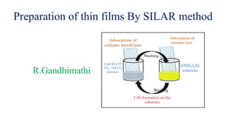
  • 7. Successive ionic layer adsorption and reaction (SILAR) ▪ Adsorptions of cations on surface of substrate ▪ Washing residue of electrolytes with the solvent ▪ Adsorptions pf anions on surface of substrate ▪ Washing residue of electrolytes with the solvent ▪ Among various chemical methods, the sequential ionic layer adsorption reaction (SILAR) has been shown to be one that most suitable for preparing semiconductor materials ▪ A facile, low-cost growth method for the fabrication semiconductors solar cells o A binary semiconductor AB, where A - cation A+ and B - anion, then ideally the lattice should have the atomic arrangement of ABABAB·····. o A SILAR process can produce such an arrangement by sequential immersion of a substrate into a cationic solution and an anionic solution o Process can be repeated to increase the amount of deposited material and the size of NCs o In a real experiment, parameters such as solution concentration, dipping time, temperature are crucial in obtaining the desired semiconductor quality
  • 8. Applications ▪ Semiconductors ▪ Oxide of metals ▪ nanocomposites ▪ polymer inorganic nanoparticles composites ▪ porous materials & nanoparticles Advantages • Excellent material utilization efficiency • Good control over the deposition process along with the film thickness • Cost effective and user friendly • Large scale deposition capability on virtually any type of substrate • Easy control on film thickness by adjusting number of deposition cycles is the beauty of this method.
  • 9. Precursors: Cadmium chloride CdCl2 solution Sodium sulphide Na2S solution Substrate: Precleaned Glass or FTO Deposition parameters for getting adherent thin films ▪ Concentration of the solution ▪ pH of the reacting baths, ▪ temperature of deposition ▪ Substrate treatment ▪ Deposition time Under optimized deposition conditions only, adherent thin films can be produced Preparation of Cadmium sulphide CdS thin films • A chemical dipping technique • Involves successive dipping of a precleaned substrate in separately placed cationic and anionic precursor • Between every immersion it is rinsed in ion exchanged water Na2S solution CdCl2 ⋅2H2O] solution Adsorption of cationic metal ions Washing Adsorption of anionic ions Reaction on the substrate lead to the formation of metal sulphide ion Washing
  • 10. Cadmium sulphide -optoelectronic applications ▪ solar cells ▪ photodiodes ▪ light emitting diodes ▪ nonlinear optics ▪ heterogeneous photocatalysis ▪ high-density magnetic information storage Precursors: Cadmium acetate Cd(CH3COO)2 ⋅2H2O] solution Ammonium sulphide [(NH4)2S] solution (OR) Sodium sulphide Na2S solution Substrate: Precleaned Glass or FTO [(NH4)2S] solution Cd(CH3CO O)2 ⋅2H2O] solution Adsorption of cationic metal ions Washing Adsorption of anionic ions CdS formation on the substrate Preparation of Cadmium sulphide CdS thin films Cd(NO2)2 Cationic solution Sodium sulphide Na2S solution Washing ▪ The characteristics of thin films are very much dependent on their thickness as the thickness of the film resolves the performance of prepared thin films ▪ Thin films surface roughness, contact angle, adhesion and intrinsic stress are the factors which decide the efficiency of the operation of any device. Significance of film thickness
  • 11. 1. Rosileschristopher, Andrea Cerdan-pasaran, Siraj Sidhik, Tzarara lopez luke , Improved performance of CdS quantum dot sensitized solar cell by solvent modified SILAR approach (2018), Solar Energy 174:240-247, DOI:10.1016/j.solener.2018.08.081 2. Partha Protim Chandra,Ayan Mukherjee, and P.Mitra, “Synthesis of Nanocrystalline CdS by SILAR and Their Characterization”, Hindawi Publishing Corporation Journal of Materials Volume 2014 3. K. Veerathangam, Muthu Senthil Pandian, P. Ramasamy, “Influence of SILAR deposition cycles in CdS quantum dot- sensitized solar cells” Journal of Materials Science: Materials in Electronics 29(9), DOI:10.1007/s10854-018-8721-0 4. B.R. Sankapal, R.S. Mane, C.D. Lokhande*, Deposition of CdS thin films by the successive ionic layer 5. adsorption and reaction (SILAR) method, Materials Research Bulletin 35 (2000) 177–184 6. B. Guzeldira, M. Saglama and A. Atesb, Deposition and Characterization of CdS, CuS and ZnS 7. Thin Films Deposited by SILAR Method, Vol. 121 (2012) ACTA PHYSICA POLONICA A No Proceedings of the International Congress on Advances in Applied Physics and Materials Science, Antalya 2011 8. Jadhav U.M.1, Patel S.N.2 and Patil R.S.1*, Room Temperature Deposition of Nanocrystalline CdS Thin Film by Successive Ionic Layer Adsorption and Reaction (SILAR) Method, Research Journal of Material Sciences Vol. 1(1), 21-25, February (2013) References