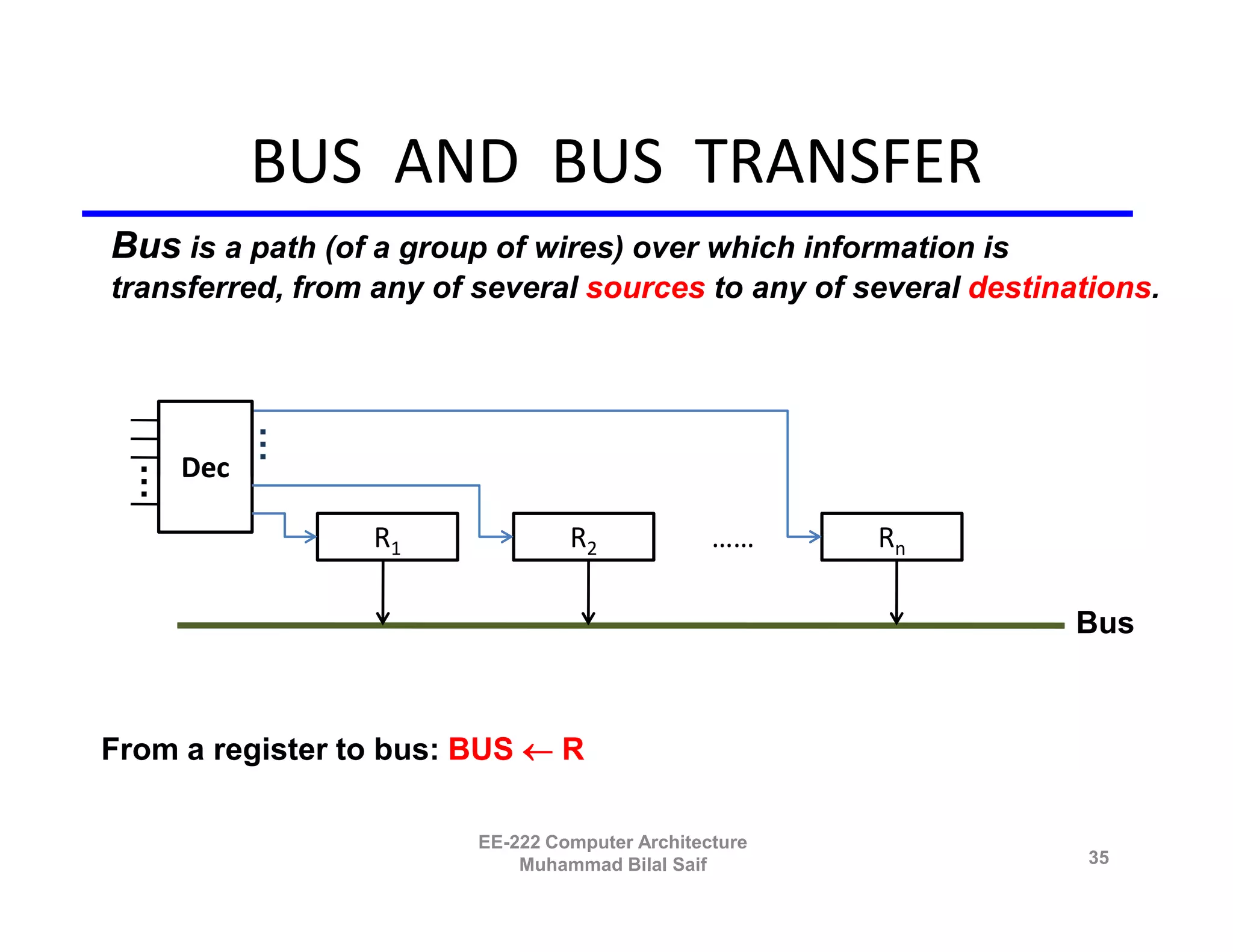
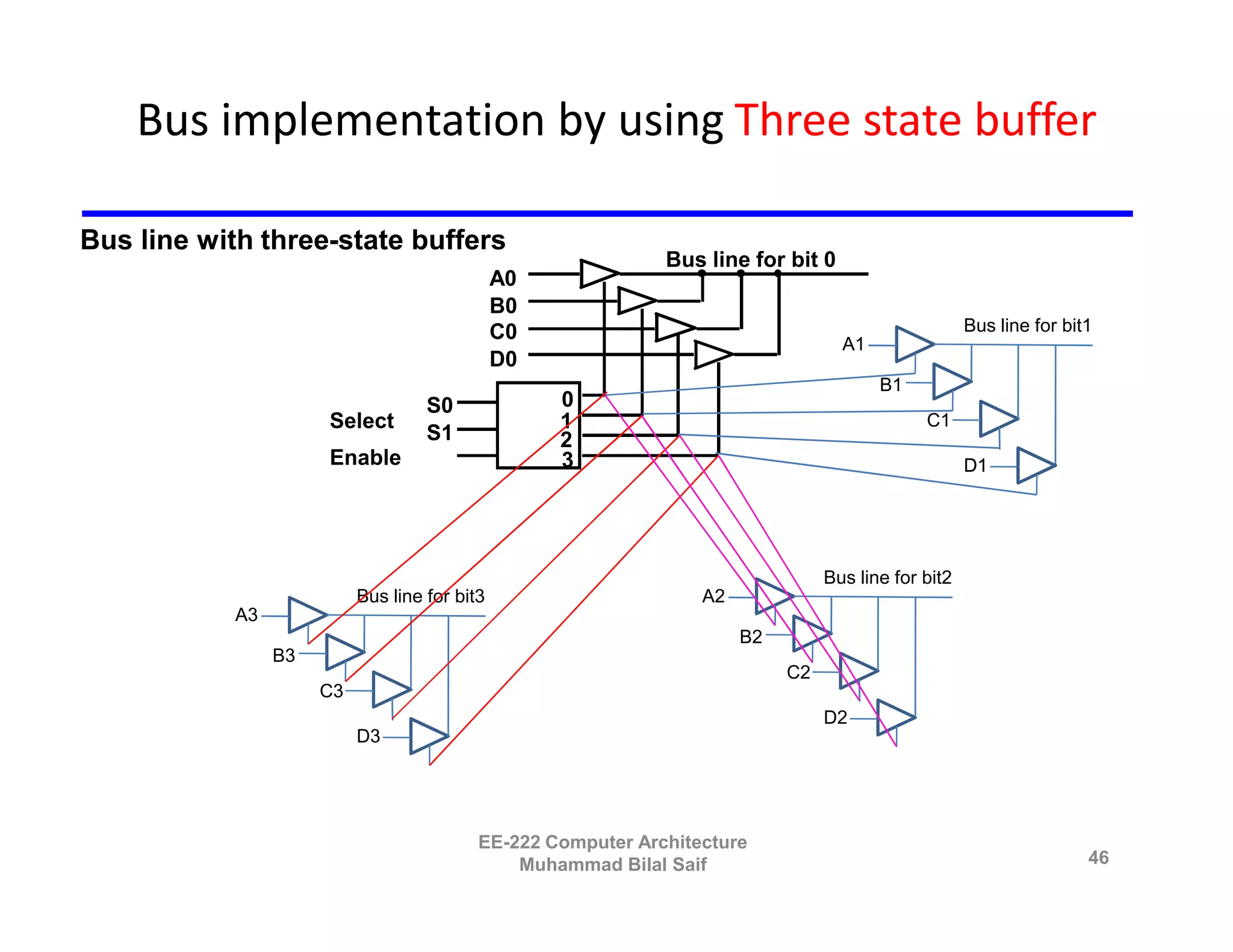
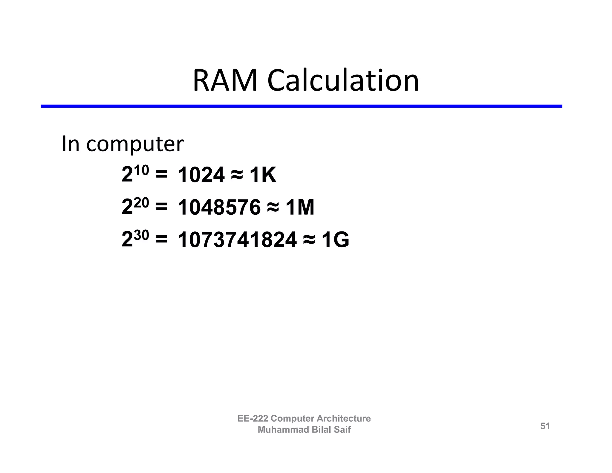
Chapter 4
Register Transfer and Microoperations
•   4-1   Register Transfer Language
•   4-2   Register Transfer
•   4-3   Bus and Memory Transfer
•   4-4   Arithmetic Microoperations
•   4-5   Logic Microoperations
•   4-6   Shift Microoperations
•   4-7   Arithmetic Logic Shift Units

                    EE-222 Computer Architecture
                        Muhammad Bilal Saif        33
CONNECTING REGISTERS
• In a digital system with many registers, it is impractical to
  have dedicated connections between all registers.
• To completely connect n registers we require n(n-1) lines
   – So this is not a realistic approach to use separate wiring for each register
     in a large digital system


• Instead, take a different approach
• Have one centralized set of circuits for data transfer – the
  bus
• Have control circuits to select which register is the source,
  and which is the destination

                            EE-222 Computer Architecture
                                Muhammad Bilal Saif                                 34
BUS AND BUS TRANSFER
Bus is a path (of a group of wires) over which information is
transferred, from any of several sources to any of several destinations.
            …
            …


      Dec
  …
  …


                  R1              R2             ……     Rn

                                                                  Bus


From a register to bus: BUS  R

                         EE-222 Computer Architecture
                             Muhammad Bilal Saif                   35
Bus Implementation
• Bus can be implemented by
1. Mux
2. Tristate buffer


               EE-222 Computer Architecture
                   Muhammad Bilal Saif        36
Bus implementation by using Mux
            Register A               Register B             Register C                 Register D
            0   1      2   3         0   1      2    3      0   1      2    3          0   1      2    3


                 B C           D0        B 1 C1      D1         B2     C2       D2         B3     C3       D3
                  0  0


            0                        0                      0                          0
                4 x1                     4 x1                   4 x1                       4 x1
                MUX                      MUX                    MUX                        MUX


0x
 select
1
0y


                                                    Register A
                                                    4-line bus C                     3rd bit of all the
 0th
   bit of all the               1st bit of all the Registers                         Registers
 Registers
                                     EE-222 Computer Architecture
                                         Muhammad Bilal Saif 2nd    bit of all the Registers                37
General rules
• A bus system will multiplex k registers of n bits
  each to produce an n-line common bus.
• The number of multiplexers needed to
  construct the bus is equal to n (# of bits on
  each register).
• The size of each multiplexer must be k x 1
  since in multiplexes k data lines.


                  EE-222 Computer Architecture
                      Muhammad Bilal Saif         38
General rule (Simplified)
• # of Mux required is equal to # of bits in each
  register.
• Size of Mux is dependent on total number of
  registers


                  EE-222 Computer Architecture
                      Muhammad Bilal Saif           39
BUS TRANSFER IN RTL
• Depending on whether the bus is to be
  mentioned explicitly or not, register transfer can
  be indicated as either
           R2 R1                                  Sout
                                                           n

                                                               Register   Bus
  or                                                 Clk
                                                                Bank
            BUS R1, R2  BUS
                                                     Sin
                                                           n


• In the former case the bus is implicit, but in the
  latter, it is explicitly indicated

                     EE-222 Computer Architecture
                         Muhammad Bilal Saif                              40
Bus implementation by using Three state buffer


       Three-State Bus Buffers


                                      0
                                      1              0
                                                     1
                                                     z        Output Y=A if C=1
                    Normal input A                            High-impedance if C=0


                    Control input C
                                      0
                                      1


In high impedance the gate acts like an open circuit.


                               EE-222 Computer Architecture
                                   Muhammad Bilal Saif                                41
Three state Bus Buffer
    • Tri-state gates can be used to implement the
      functioning of any other conventional gate
      such as AND, OR, NAND, NOR etc.


Assignment # 02:
a) Draw the circuit, which performs the functionality of OR gate, by using only
   tri-state buffers and resistors.
b) Repeat the above for NOR gate
                              EE-222 Computer Architecture
                                  Muhammad Bilal Saif                     42
Three states gates in Verilog


         EE-222 Computer Architecture
             Muhammad Bilal Saif        44
Syntax of three state gates


        EE-222 Computer Architecture
            Muhammad Bilal Saif        45
Bus implementation by using Three state buffer

Bus line with three-state buffers
                                                              Bus line for bit 0
                                               A0
                                               B0
                                               C0                                                    Bus line for bit1
                                                                                   A1
                                               D0
                                                                                        B1
                                    S0              0
                      Select                        1                                         C1
                                    S1              2
                      Enable                        3                                                D1


                                                                                 Bus line for bit2
                           Bus line for bit3                      A2
            A3
                                                                       B2
                 B3
                                                                            C2
                      C3
                                                                                 D2
                           D3


                                           EE-222 Computer Architecture
                                               Muhammad Bilal Saif                                                   46
General Rule
• In case of three state buffers; a common bus
  for k registers of n bits each, can be
  constructed by using n circuits with k buffer in
  each as shown in the previous slide.
• Only one decoder is required.


                  EE-222 Computer Architecture
                      Muhammad Bilal Saif        47
Surprise Quiz - 01
• Draw the diagram of a bus system by using tri-
  state buffers, having
  – 4 registers of 2 bits each.


                    EE-222 Computer Architecture
                        Muhammad Bilal Saif        48
Simple RAM design
Control Signals
                         Read/Write Control
                                                                     8

                                               8 bit Register
Address Bus       2
                                               8 bit Register
                           Dec
                                               8 bit Register

                                               8 bit Register


                                                                Data Bus
                      In terms of RAM, each internal
                      register is called a “word”
                                 EE-222 Computer Architecture
                                     Muhammad Bilal Saif                   49
MEMORY (RAM)
• Assume the RAM contains 2k words and each word
  has n bits. It needs the following
  –   n data input lines
  –   n data output lines
                                                                  data input lines
  –   k address lines
                                                                           n
  –   A Read control line
  –   A Write control line                    address lines
                                                              k
                                                                       RAM
                                                Read
                                                                       unit
                                                Write

                                                                            n
                                                                  data output lines


                             EE-222 Computer Architecture
                                 Muhammad Bilal Saif                                 50
RAM Calculation
In computer
     210 = 1024 ≈ 1K
     220 = 1048576 ≈ 1M
     230 = 1073741824 ≈ 1G


                EE-222 Computer Architecture
                    Muhammad Bilal Saif        51
MEMORY TRANSFER
    • Collectively, the memory is viewed at the register level as
      a device, “M”.
    • Since it contains multiple locations, we must specify
      which address in memory we will be using
    • Memory is usually accessed in computer systems by
      putting the desired address in a special register, the
      Memory Address Register (MAR, or AR)
    • When memory is accessed, the contents of the MAR get
      sent to the memory unit’s address lines              M
                                                                     Memory             Read
                                           MAR / AR
                                                                      unit              Write
Further material regarding memory can be found at
article 2-7, p59 of text book                                     Data out    Data in
                                   EE-222 Computer Architecture
                                       Muhammad Bilal Saif                              52
MEMORY READ
• To read a value from a location in memory and load it into a register,
  the register transfer language notation looks like this:

                     R1  M[MAR]

• This causes the following actions to occur
    –   The contents of the MAR get sent to the memory address lines
    –   A Read (= 1) gets sent to the memory unit
    –   The contents of the specified address are put on the memory’s output data lines
    –   These get sent over the bus to be loaded into register R1


                             EE-222 Computer Architecture
                                 Muhammad Bilal Saif                                      53
MEMORY WRITE

• To write a value from a register to a location in memory looks like
  this in register transfer language:

                      M[MAR]  R1

• This causes the following to occur
    – The contents of the MAR get sent to the memory address lines
    – The values in register R1 get sent over the bus to the data input lines of the
      memory
    – A Write (= 1) gets sent to the memory unit
    – The values get loaded into the specified address in the memory


                             EE-222 Computer Architecture
                                 Muhammad Bilal Saif                                   54
SUMMARY OF R. TRANSFER MICROOPERATIONS

A B            Transfer content of reg. B into reg. A
AR DR(AD)     Transfer content of AD portion of reg. DR into reg. AR
A  constant   Transfer a binary constant into reg. A
BUS  R1,       Transfer content of R1 into bus and, at the same time,
R2 BUS          transfer content of bus into R2
AR              Address register
DR              Data register
M[AR]           Memory word specified by reg. AR
M               Equivalent to M[AR]
DR  M         Memory read operation: transfers content of
                     memory word specified by AR into DR
M  DR         Memory write operation: transfers content of
                     DR into memory word specified by AR


                      EE-222 Computer Architecture
                          Muhammad Bilal Saif                       55
Chapter 4
Register Transfer and Microoperations
•   4-1   Register Transfer Language
•   4-2   Register Transfer
•   4-3   Bus and Memory Transfer
•   4-4   Arithmetic Microoperations
•   4-5   Logic Microoperations
•   4-6   Shift Microoperations
•   4-7   Arithmetic Logic Shift Units

                    EE-222 Computer Architecture
                        Muhammad Bilal Saif        56
MICROOPERATIONS
• Computer system microoperations are of four
  types:
  – Register transfer microoperations
  – Arithmetic microoperations                   We have covered this topic;
                                                 this microoperation does
  – Logic microoperations                        not alter the register
                                                 contents while transfer
  – Shift microoperations

                                                 These operations change
                                                 the register contents while
                                                 transfer
                  EE-222 Computer Architecture
                      Muhammad Bilal Saif                               57
ARITHMETIC MICROOPERATIONS
• The basic arithmetic microoperations are
    –   Addition
    –   Subtraction
    –   Increment                               Can be implemented by
    –   Decrement                               1. Binary up/down
                                                 Subtraction is achieved
                                                 by counter i.e.
                                                    addition
• The additional arithmetic microoperations are
   – Add with carry                             2. Adding/subtracting 1
                                                 R3R1 + R2’ + 1
    – Subtract with borrow
    – Transfer/Load
    – etc. …

                 Summary of Typical Arithmetic Micro-Operations
        R3  R1 + R2        Contents of R1 plus R2 transferred to R3
        R3  R1 - R2        Contents of R1 minus R2 transferred to R3
        R2  R2’            Complement the contents of R2
        R2  R2’+ 1         2's complement the contents of R2 (negate)
        R3  R1 + R2’+ 1    subtraction
        R1  R1 + 1         Increment
        R1  R1 - 1         Decrement
                                 EE-222 Computer Architecture
                                     Muhammad Bilal Saif                  58
BINARY ADDER
For add microoperation we require
•Registers that hold the data
•Digital components that perform the addition (Full adder)

                        B3        A3        B2        A2        B1        A1        B0        A0

   Binary Adder
                             FA        C3        FA        C2        FA        C1        FA        C0


                  C4         S3                  S2                  S1                  S0


For n bit binary adder, we require n full adders.


                                  EE-222 Computer Architecture
                                      Muhammad Bilal Saif                                               59

Lecture 2

  • 1.
    Chapter 4 Register Transferand Microoperations • 4-1 Register Transfer Language • 4-2 Register Transfer • 4-3 Bus and Memory Transfer • 4-4 Arithmetic Microoperations • 4-5 Logic Microoperations • 4-6 Shift Microoperations • 4-7 Arithmetic Logic Shift Units EE-222 Computer Architecture Muhammad Bilal Saif 33
  • 2.
    CONNECTING REGISTERS • Ina digital system with many registers, it is impractical to have dedicated connections between all registers. • To completely connect n registers we require n(n-1) lines – So this is not a realistic approach to use separate wiring for each register in a large digital system • Instead, take a different approach • Have one centralized set of circuits for data transfer – the bus • Have control circuits to select which register is the source, and which is the destination EE-222 Computer Architecture Muhammad Bilal Saif 34
  • 3.
    BUS AND BUSTRANSFER Bus is a path (of a group of wires) over which information is transferred, from any of several sources to any of several destinations. … … Dec … … R1 R2 …… Rn Bus From a register to bus: BUS  R EE-222 Computer Architecture Muhammad Bilal Saif 35
  • 4.
    Bus Implementation • Buscan be implemented by 1. Mux 2. Tristate buffer EE-222 Computer Architecture Muhammad Bilal Saif 36
  • 5.
    Bus implementation byusing Mux Register A Register B Register C Register D 0 1 2 3 0 1 2 3 0 1 2 3 0 1 2 3 B C D0 B 1 C1 D1 B2 C2 D2 B3 C3 D3 0 0 0 0 0 0 4 x1 4 x1 4 x1 4 x1 MUX MUX MUX MUX 0x select 1 0y Register A 4-line bus C 3rd bit of all the 0th bit of all the 1st bit of all the Registers Registers Registers EE-222 Computer Architecture Muhammad Bilal Saif 2nd bit of all the Registers 37
  • 6.
    General rules • Abus system will multiplex k registers of n bits each to produce an n-line common bus. • The number of multiplexers needed to construct the bus is equal to n (# of bits on each register). • The size of each multiplexer must be k x 1 since in multiplexes k data lines. EE-222 Computer Architecture Muhammad Bilal Saif 38
  • 7.
    General rule (Simplified) •# of Mux required is equal to # of bits in each register. • Size of Mux is dependent on total number of registers EE-222 Computer Architecture Muhammad Bilal Saif 39
  • 8.
    BUS TRANSFER INRTL • Depending on whether the bus is to be mentioned explicitly or not, register transfer can be indicated as either R2 R1 Sout n Register Bus or Clk Bank BUS R1, R2  BUS Sin n • In the former case the bus is implicit, but in the latter, it is explicitly indicated EE-222 Computer Architecture Muhammad Bilal Saif 40
  • 9.
    Bus implementation byusing Three state buffer Three-State Bus Buffers 0 1 0 1 z Output Y=A if C=1 Normal input A High-impedance if C=0 Control input C 0 1 In high impedance the gate acts like an open circuit. EE-222 Computer Architecture Muhammad Bilal Saif 41
  • 10.
    Three state BusBuffer • Tri-state gates can be used to implement the functioning of any other conventional gate such as AND, OR, NAND, NOR etc. Assignment # 02: a) Draw the circuit, which performs the functionality of OR gate, by using only tri-state buffers and resistors. b) Repeat the above for NOR gate EE-222 Computer Architecture Muhammad Bilal Saif 42
  • 11.
    Three states gatesin Verilog EE-222 Computer Architecture Muhammad Bilal Saif 44
  • 12.
    Syntax of threestate gates EE-222 Computer Architecture Muhammad Bilal Saif 45
  • 13.
    Bus implementation byusing Three state buffer Bus line with three-state buffers Bus line for bit 0 A0 B0 C0 Bus line for bit1 A1 D0 B1 S0 0 Select 1 C1 S1 2 Enable 3 D1 Bus line for bit2 Bus line for bit3 A2 A3 B2 B3 C2 C3 D2 D3 EE-222 Computer Architecture Muhammad Bilal Saif 46
  • 14.
    General Rule • Incase of three state buffers; a common bus for k registers of n bits each, can be constructed by using n circuits with k buffer in each as shown in the previous slide. • Only one decoder is required. EE-222 Computer Architecture Muhammad Bilal Saif 47
  • 15.
    Surprise Quiz -01 • Draw the diagram of a bus system by using tri- state buffers, having – 4 registers of 2 bits each. EE-222 Computer Architecture Muhammad Bilal Saif 48
  • 16.
    Simple RAM design ControlSignals Read/Write Control 8 8 bit Register Address Bus 2 8 bit Register Dec 8 bit Register 8 bit Register Data Bus In terms of RAM, each internal register is called a “word” EE-222 Computer Architecture Muhammad Bilal Saif 49
  • 17.
    MEMORY (RAM) • Assumethe RAM contains 2k words and each word has n bits. It needs the following – n data input lines – n data output lines data input lines – k address lines n – A Read control line – A Write control line address lines k RAM Read unit Write n data output lines EE-222 Computer Architecture Muhammad Bilal Saif 50
  • 18.
    RAM Calculation In computer 210 = 1024 ≈ 1K 220 = 1048576 ≈ 1M 230 = 1073741824 ≈ 1G EE-222 Computer Architecture Muhammad Bilal Saif 51
  • 19.
    MEMORY TRANSFER • Collectively, the memory is viewed at the register level as a device, “M”. • Since it contains multiple locations, we must specify which address in memory we will be using • Memory is usually accessed in computer systems by putting the desired address in a special register, the Memory Address Register (MAR, or AR) • When memory is accessed, the contents of the MAR get sent to the memory unit’s address lines M Memory Read MAR / AR unit Write Further material regarding memory can be found at article 2-7, p59 of text book Data out Data in EE-222 Computer Architecture Muhammad Bilal Saif 52
  • 20.
    MEMORY READ • Toread a value from a location in memory and load it into a register, the register transfer language notation looks like this: R1  M[MAR] • This causes the following actions to occur – The contents of the MAR get sent to the memory address lines – A Read (= 1) gets sent to the memory unit – The contents of the specified address are put on the memory’s output data lines – These get sent over the bus to be loaded into register R1 EE-222 Computer Architecture Muhammad Bilal Saif 53
  • 21.
    MEMORY WRITE • Towrite a value from a register to a location in memory looks like this in register transfer language: M[MAR]  R1 • This causes the following to occur – The contents of the MAR get sent to the memory address lines – The values in register R1 get sent over the bus to the data input lines of the memory – A Write (= 1) gets sent to the memory unit – The values get loaded into the specified address in the memory EE-222 Computer Architecture Muhammad Bilal Saif 54
  • 22.
    SUMMARY OF R.TRANSFER MICROOPERATIONS A B Transfer content of reg. B into reg. A AR DR(AD) Transfer content of AD portion of reg. DR into reg. AR A  constant Transfer a binary constant into reg. A BUS  R1, Transfer content of R1 into bus and, at the same time, R2 BUS transfer content of bus into R2 AR Address register DR Data register M[AR] Memory word specified by reg. AR M Equivalent to M[AR] DR  M Memory read operation: transfers content of memory word specified by AR into DR M  DR Memory write operation: transfers content of DR into memory word specified by AR EE-222 Computer Architecture Muhammad Bilal Saif 55
  • 23.
    Chapter 4 Register Transferand Microoperations • 4-1 Register Transfer Language • 4-2 Register Transfer • 4-3 Bus and Memory Transfer • 4-4 Arithmetic Microoperations • 4-5 Logic Microoperations • 4-6 Shift Microoperations • 4-7 Arithmetic Logic Shift Units EE-222 Computer Architecture Muhammad Bilal Saif 56
  • 24.
    MICROOPERATIONS • Computer systemmicrooperations are of four types: – Register transfer microoperations – Arithmetic microoperations We have covered this topic; this microoperation does – Logic microoperations not alter the register contents while transfer – Shift microoperations These operations change the register contents while transfer EE-222 Computer Architecture Muhammad Bilal Saif 57
  • 25.
    ARITHMETIC MICROOPERATIONS • Thebasic arithmetic microoperations are – Addition – Subtraction – Increment Can be implemented by – Decrement 1. Binary up/down Subtraction is achieved by counter i.e. addition • The additional arithmetic microoperations are – Add with carry 2. Adding/subtracting 1 R3R1 + R2’ + 1 – Subtract with borrow – Transfer/Load – etc. … Summary of Typical Arithmetic Micro-Operations R3  R1 + R2 Contents of R1 plus R2 transferred to R3 R3  R1 - R2 Contents of R1 minus R2 transferred to R3 R2  R2’ Complement the contents of R2 R2  R2’+ 1 2's complement the contents of R2 (negate) R3  R1 + R2’+ 1 subtraction R1  R1 + 1 Increment R1  R1 - 1 Decrement EE-222 Computer Architecture Muhammad Bilal Saif 58
  • 26.
    BINARY ADDER For addmicrooperation we require •Registers that hold the data •Digital components that perform the addition (Full adder) B3 A3 B2 A2 B1 A1 B0 A0 Binary Adder FA C3 FA C2 FA C1 FA C0 C4 S3 S2 S1 S0 For n bit binary adder, we require n full adders. EE-222 Computer Architecture Muhammad Bilal Saif 59