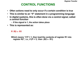
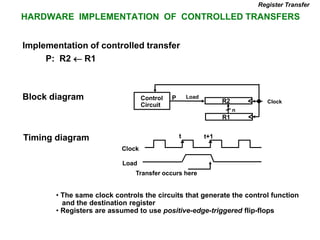
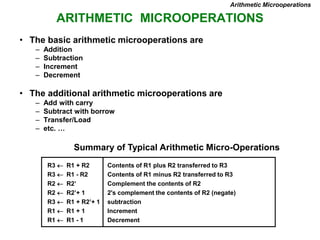
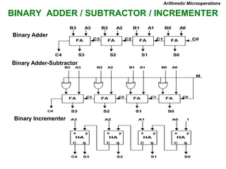
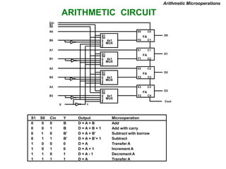
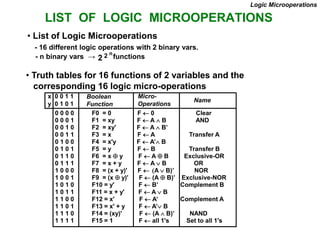
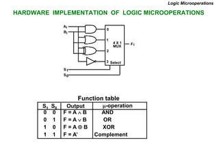
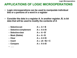
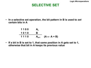
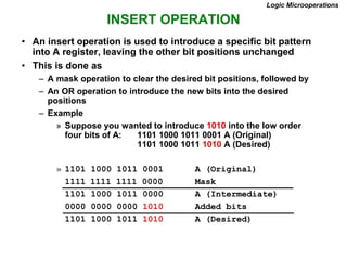
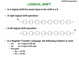
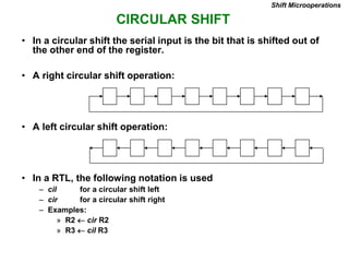
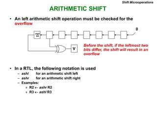
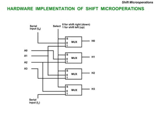
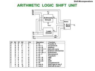
This document provides information about register transfer and microoperations in a computer organization and architecture course. It defines register transfer as copying the contents of one register to another and describes various types of microoperations including register transfer, arithmetic, logic, and shift microoperations. It explains how registers are designated in register transfer language and how operations between registers are represented.

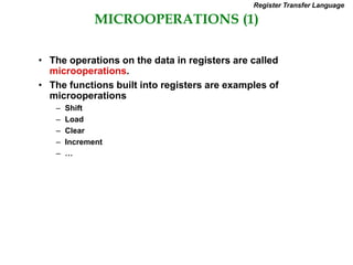

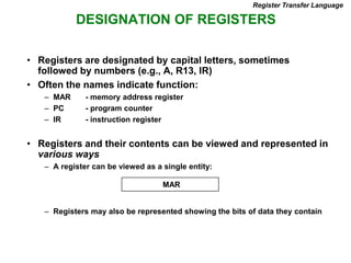
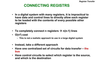
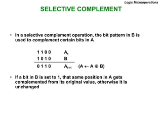
![MEMORY READ
Bus and Memory Transfers
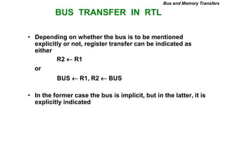
• To read a value from a location in memory and load it into
a register, the register transfer language notation looks
like this:
• This causes the following to occur
– The contents of the MAR get sent to the memory address lines
– A Read (= 1) gets sent to the memory unit
– The contents of the specified address are put on the memory’s
output data lines
– These get sent over the bus to be loaded into register R1
R1 M[MAR]](https://image.slidesharecdn.com/unit-230413165738-aa2c7b50/85/coa-25-320.jpg)
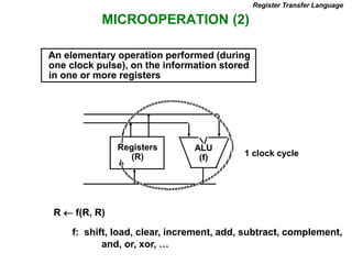
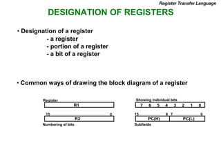
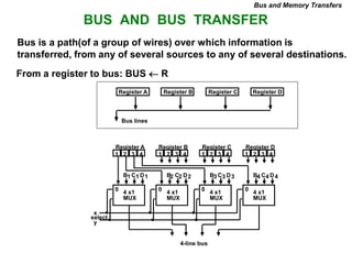
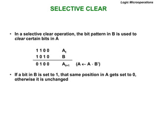
![MEMORY WRITE
Bus and Memory Transfers
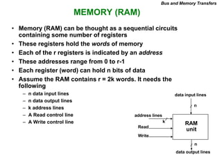
• To write a value from a register to a location in memory
looks like this in register transfer language:
• This causes the following to occur
– The contents of the MAR get sent to the memory address lines
– A Write (= 1) gets sent to the memory unit
– The values in register R1 get sent over the bus to the data input lines
of the memory
– The values get loaded into the specified address in the memory
M[MAR] R1](https://image.slidesharecdn.com/unit-230413165738-aa2c7b50/85/coa-26-320.jpg)
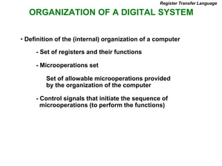
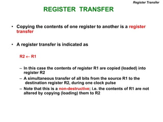
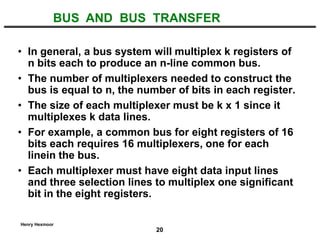
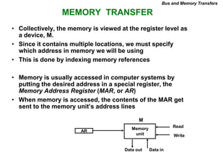
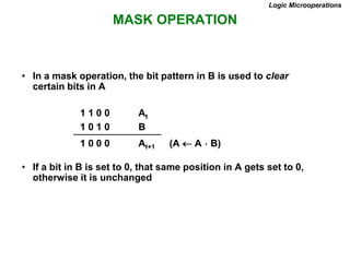
![SUMMARY OF R. TRANSFER MICROOPERATIONS
Bus and Memory Transfers
A B Transfer content of reg. B into reg. A
AR DR(AD) Transfer content of AD portion of reg. DR into reg. AR
A constant Transfer a binary constant into reg. A
ABUS R1, Transfer content of R1 into bus A and, at the same time,
R2 ABUS transfer content of bus A into R2
AR Address register
DR Data register
M[R] Memory word specified by reg. R
M Equivalent to M[AR]
DR M Memory read operation: transfers content of
memory word specified by AR into DR
M DR Memory write operation: transfers content of
DR into memory word specified by AR](https://image.slidesharecdn.com/unit-230413165738-aa2c7b50/85/coa-27-320.jpg)


![Getting Started with Apache Spark: Big Data Made Simple [Free Meetup]](https://cdn.slidesharecdn.com/ss_thumbnails/apachesparkgettingstarted-260203175547-8361bcc3-thumbnail.jpg?width=640&height=640&fit=bounds)
