
Recommended
More Related Content
What's hot
What's hot (19)
Similar to Data transfer scheme
Similar to Data transfer scheme (20)
Recently uploaded
Recently uploaded (20)
Data transfer scheme
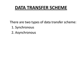
- 1. DATA TRANSFER SCHEME There are two types of data transfer scheme: 1. Synchronous 2. Asynchronous
- 2. Synchronous input / output transfer • Common clock signal is used. • At time t₀ the processor places the device address on the address lines of system bus. • During time t₀-t₁, address device gets the address & it recognize that an input operation is requested.
- 3. CONTINUED… • At time t₁, address device places its data on the data bus. At the end of the bus cycle i.e, at t₂ the processor reads the data lines & loads the data from data bus into its input buffer. • For output processor places the output data on data line. • At t₁ - Device reads the data line and load data into its data buffer. • At t₂ - Output have been received by the IO device and the cycle ends.
- 4. ASYNCHRONOUS INPUT/OUTPUT TRANSFER • The clock line replaced by two control signal ready and accept. • For input operation, processor places the address & sets the control lines to perform the input operation. • Ready line activated – Addressed device ready to accept data. • Addressed device place data on data accept line activated. • Processor load data on input buffer.
- 5. CONTINUED… For output operation: • Processor places the address, data and sets the control line to perform the output operation. • It then indicates the addressed device that it has send data by activating Ready signal. • The addressed device reads data into its input buffer when it receive ready signal. It then indicates that it has done so by the Accept signal.