1. Basic Electronics
(Module 1 – Semiconductor Diodes)
Dr. Chitralekha Mahanta
Department of Electronics and Communication Engineering.
Indian Institute of Technology, Guwahati
Lecture - 1
Semiconductor Materials: Intrinsic and Extrinsic
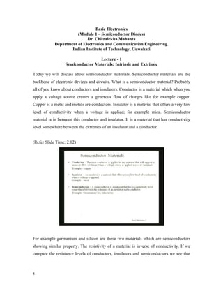
Today we will discuss about semiconductor materials. Semiconductor materials are the
backbone of electronic devices and circuits. What is a semiconductor material? Probably
all of you know about conductors and insulators. Conductor is a material which when you
apply a voltage source creates a generous flow of charges like for example copper.
Copper is a metal and metals are conductors. Insulator is a material that offers a very low
level of conductivity when a voltage is applied; for example mica. Semiconductor
material is in between this conductor and insulator. It is a material that has conductivity
level somewhere between the extremes of an insulator and a conductor.
(Refer Slide Time: 2:02)
For example germanium and silicon are these two materials which are semiconductors
showing similar property. The resistivity of a material is inverse of conductivity. If we
compare the resistance levels of conductors, insulators and semiconductors we see that
1
2. the conductor has resistivity value which is the least among the three. That is, a copper
which is a conductor has a maximum conductivity so its resistivity value is around 10-6
ohm centimeter whereas an insulator has a resistivity of 1012
ohm centimeter. This is
much more than conductor but semiconductor like germanium and silicon have resistivity
values in between these two. For example if we consider germanium semiconductor it has
resistivity value of 50 ohm centimeter and silicon has resistivity value of 50 x 103
ohm
centimeter.
(Refer Slide Time: 3:20)
You can see that semiconductor has resistivity in between conductor and insulator. If we
consider these three, i.e insulators, conductors and semiconductors and see their energy
band diagrams, then we find that the energy gap between the valence band and the
conduction band in an insulator is very high.
2
3. (Refer Slide Time: 3:50)
It is around 6 electron volts as is seen here. This energy gap means it is a forbidden band
and the electrons will have to acquire this much of energy to become conductive and
enter the conduction band. But semiconductor does not have such a high forbidden
energy gap which is around 1 electron volt as is seen here. Electrons can acquire that
much of energy which is 1 electron volt only to jump from valence band to the
conduction band in order to become conductive and metals like copper which are
conductors have overlapping conduction band and valence band and they have zero
electron volt. That is why they conduct because electrons can very easily shift between
valence band and conduction band and take part in conduction. Semiconductor is a
material that has conductivity level between the extremes of insulator and conductor and
why this is so?
3
4. (Refer Slide Time: 5:02)
That is because the semiconductor like germanium and silicon have some unique
qualities which are due to their position in the periodic table and their atomic structure.
These are group IV elements. The atoms of these materials like germanium and silicon
have a very different and definite pattern that is periodic in nature. That is it continuously
repeats itself and one complete pattern is called a crystal and the periodic arrangement of
the atoms is a lattice. Both germanium and silicon have 4 electrons in the outer most orbit
which are called valence electrons. In order to complete the structure of inert gas they
will always try to complete the 8 electrons in the outer most orbit.
4
5. (Refer Slide Time: 6:01)
In the pure germanium or silicon crystal these 4 valence electrons will be bonded to 4
neighboring atoms as shown in this diagram. If I consider a germanium atom it has 1, 2,
3, 4 electrons in the outer most orbit which are called valence electrons. Similarly silicon
will also have 4 electrons in the outer most orbit because they are group IV materials.
(Refer Slide Time: 6:35)
5
6. They will try to complete the 8 electron structure. That is why they will share electrons
with the neighboring atoms as is seen here. If we consider silicon atom, these 4 electrons
in the outermost orbit are sharing electrons among themselves so that the total number
becomes 4 and 4, 8. These atoms which are nearby are sharing these covalent bonds.
(Refer Slide Time: 7:13)
These covalent bonds are formed between neighboring atoms of silicon and thereby they
complete the structure of the inert gas having 8 electrons in the outermost orbit so that
they become stable. These semiconductors which are in the purest form are known as
intrinsic semiconductors. In these intrinsic semiconductors the free electrons are due to
only natural causes like thermal energy or light energy which impart extra energy to the
electrons to become free and thereby they get additional kinetic energy from these natural
causes and they break this covalent bond. These covalent bonds will break in order to
become free. 1 electron will become free when it absorbs kinetic energy from either the
surrounding or any light is falling on them.
6
7. (Refer Slide Time: 8:19)
An increase in temperature is naturally the reason for more conductivity in
semiconductors. This increase in temperature of a semiconductor results in increase in the
number of free electrons in the material so they become more and more conductive. Even
though they may be not so conductive at certain temperature but if we increase the
temperature they will absorb more kinetic energy and will become more conductive. The
semiconductors like germanium and silicon they have negative temperature coefficient as
the resistance will decrease with increase in temperature. This is a peculiar phenomena
that is seen in semiconductors which is just opposite to your conductors like metal.
We have been talking about the intrinsic semiconductors. Those are the purest form of
semiconductors without any impurity in them. But there is another type of semiconductor
which is extrinsic semiconductor.
7
8. (Refer Slide Time: 9:26)
This extrinsic semiconductor has the characteristics such that their property can be
significantly altered by addition of certain impurity atoms into the pure semiconductor
material. The impurities added to the purest semiconductor to make an intrinsic into
extrinsic semiconductor are defined. We can add pentavalent impurity materials like
antimony, arsenic and phosphorous which are group V elements and have 5 electrons in
the outer most orbit or we can add trivalent materials like boron, gallium and indium
which are group III materials and have 3 electrons in their outer most orbit and the
standard norm of adding is that they are added 1 part in 10 millions. That is to 10 million
atoms of intrinsic semiconductor you add one impurity atom.
We will discuss how the addition of this impurity totally changes the electrical properties
of the intrinsic semiconducting material. When certain impurity atoms like antimony or
boron are added to a pure semiconductor material we get an extrinsic semiconductor and
this process of adding certain impurity atoms like antimony or boron into pure
semiconductor like silicon is called the doping process. As a result of this doping we get
extrinsic semiconductor either n-type or p-type.
8
9. (Refer Slide Time: 11:19)
That is you can get n-type extrinsic semiconductor if you add pentavalent impurity
material like antimony or phosphorous into a pure semiconductor like germanium or
silicon or you can have p-type extrinsic semiconductor when you add trivalent impurity
material like boron or indium into a pure germanium or silicon semiconductor.
What happens when you add an impurity atom to a pure semiconductor? Let us take for
example an n-type semiconductor. How it is formed? N-type semiconductor means we
have to add pentavalent impurity material. Let us take the example of adding antimony
which is a pentavalent impurity material which is a group V material having 5 electrons
in the outer most orbit to a silicon semiconductor. This silicon atom has 4 electrons in the
outer most orbit. These are silicon outermost orbit electrons and now as we have added 1
antimony atom which has 5 electrons in the outer most orbit, it will share these electrons
with the silicon atoms and these covalent bonds will be completed. 4 and 4, 8 electrons
are there so these covalent bonds will be completed. But then 1 electron is in excess. That
is it is extra. This fifth electron is donated by this antimony atom. This fifth electron is
free. It can take part in conduction easily. That is why it is donating 1 electron. It is
excess of 1 electron which is negatively charged.
9
10. (Refer Slide Time: 13:22)
This is called n-type semiconductor. What happens when we add p-type semiconductor?
We have seen how n-type semiconductor is formed by adding pentavalent impurity
material to intrinsic semiconductor like germanium or silicon. Let us see how p-type
semiconductor is formed from pure semiconductor like germanium or silicon by adding
trivalent impurity material like boron or indium. Let us add boron impurity which is a
group III material having 3 electrons in the outer most orbit to a silicon semiconductor.
This boron has 3 electrons in the outer most orbit. It will complete its covalent bond with
neighboring silicon atom having shared these 2 electrons as is seen here. These 2
electrons will form a covalent bond. In this process 3 covalent bonds are now completed.
What about the other covalent bond? This covalent bond is now devoid or it is short of 1
electron to complete its covalent bond. This shortage of 1 electron means it is having less
negative charge. This less negative charge or a positive charge is there in this covalent
bond. This is called a hole. Hole means it is basically devoid of 1 electron. So there is a
hole formed here in this covalent bond and this hole is a positively charged particle.
10
11. (Refer Slide Time: 15:21)
So this p- type semiconductor basically is formed in this way which will have holes as
charge carriers.
If we consider again the n-type material we have seen that in n-type material which is an
extrinsic semiconductor it has donated 1 electron. As it has donated 1 electron, the atom
of this extrinsic semiconductor is now having 1 positive charge which is called an ion. 1
atom of this extrinsic semiconductor when it donates one electron it becomes ion having
1 positive charge which is shown here. The donor ions are having 1 positive charge and
there will be electrons which are in abundance in the n-type material. These are called
majority carriers. In an n-type material the majority carriers are electrons but there will
also be in less number the minority carriers which are holes. These holes will be from this
intrinsic material that is coming. If n-type material is considered altogether we will see
majority carriers as electrons, minority carriers as holes and immobile ions which are
positively charged or donor ions.
11
12. (Refer Slide Time: 17:03)
This is the structure of n-type material. Similarly if we consider a p-type material, p-type
material has acceptor ions. In the p-type material we have seen that there is a hole and as
it is devoid of an electron it will be always trying to get an electron from the
neighborhood atoms. The electron from the neighborhood atom will come and fill up this
hole and as a result this boron atom will be negatively charged. It is accepting 1 electron
so it will be negatively charged.
12
13. (Refer Slide Time: 17:45)
That means in a p-type material the atom of the impurity will be an acceptor ion having a
negative charge and there will be holes which are positively charged as majority carriers
and also very less in numbers although there will be presence of minority carriers which
are electrons which are coming from the intrinsic semiconductor. This is p-type material
where all these carriers and ions you see here. We can summarize that in n-type
semiconductor the majority carriers are electrons and minority carriers are holes and in p-
type semiconductor majority carriers are holes but minority carriers are electrons.
13
14. (Refer Slide Time: 18:39)
These are the charge carriers available in n-type and p-type semiconductors. How does
the current flow in a semiconductor? Current flow is due to the movement of electrons
and conventional current is always against the direction of movement of electrons.
Suppose if electron moves in this way then conventional current direction will be in
opposite way. This is electron movement direction and this is conventional current
direction. But we have seen that another type of charge carrier is also there in
semiconductors which are holes and which are positively charged. So the current flow
will be now due to these two types of carriers; one is electron and other is hole and both
are opposite in charge. That is electron is negatively charged and hole is positively
charged.
We are having a semiconductor. We have the silicon atom and this is an impurity atom
which is boron. It is creating a hole as is seen here. In order to fill up this hole electron
from a neighboring atom will come. This movement of electron will be in this direction.
When this electron comes and fills up this hole then this place will be now devoid of
electron. It will be now a hole. Now hole movement will be from this position to this
position. It is just opposite to the electron movement. Electron movement is in the
direction of this solid arrow and hole movement is in the direction of this dotted arrow. If
14
15. we consider the conventional current direction which is opposite to the direction of
movement of electrons, then the current direction will be in the same direction, because
of both these components. If I consider conventional current direction it will be like this
because this electron movement is in this direction and hole movement is in opposite
direction. But the final direction of current flow is opposite to the electron movement.
(Refer Slide Time: 21:27)
So it will be in opposition to this movement of electron but that is the same direction of
the hole movement. We will discuss a very fundamental and very important law which
gives the relationship between electron and hole concentration and that is known as mass
action law. What is that law? It states that under thermal equilibrium the product of the
free negative and positive concentrations is a constant independent of the amount of
donor and acceptor impurity doping. That is mathematically if you write np is equal to ni
square where n is the concentration of free electrons in thermal equilibrium, p is the
concentration of holes in thermal equilibrium and ni is the intrinsic carrier concentration.
15
16. (Refer Slide Time: 22:27)
This is a very fundamental law in electronics which is mass action law. Now let us
consider about the charge densities in a semiconductor. We will consider charge density
later. Before that you must also know what is the law of electrical neutrality that is
satisfied in the semiconductor? Let us consider a semiconductor material and consider a
situation where it is doped by both n-type and p-type materials and let ND be the
concentration of donor atoms. These donor atoms are all ionized and already we have
seen that these will be positively charged donor atoms. We have ND positive charges per
cubic meter which are contributed by these donor ions and let p be the hole concentration
in the semiconductor so that the total positive charge density in the semiconductor is ND
plus p. That is total positive charge density in the semiconductor which is contributed by
donor atoms as well as holes. Similarly if we consider that NA is the concentration of
acceptor ions then these contribute NA negative charges per cubic meter and let small n
be the electron concentration in the semiconductor. So the total negative charge density in
the semiconductor will be now NA plus n and since the semiconductor is electrically
neutral we have this law to be satisfied that ND plus p is equal to NA plus n. Let us
number this equation as 2.
16
17. (Refer Slide Time: 24:24)
That means this electrical neutrality must be satisfied in a semiconductor given by this
equation. Consider solely n-type material. We can either dope by n-type or by p-type
impurity. So in an n-type material doping NA will be zero and then the equation 2 will be
now ND plus p is equal to n since NA is equal to zero or ND is equal to n minus p. As it is
an n-type material the concentration of electrons is much much more than concentration
of the holes. So n minus p we can roughly say that equal to n. Then from this equation we
will get that the electron concentration is almost equal to the concentration of the donor
atoms ND and if we use a subscript small n, the electron concentration in an n-type
material nn is equal to capital N subscript capital D. From this equation we can get now
hole concentration for this n-type material which is given by pn is equal to ni square by
ND. Here we are using equation number 1, mass action law.
17
18. (Refer Slide Time: 25:51)
Similarly if we consider a p-type material, the donor concentration is zero since it is a p-
type material. So the equation 2 will be now reduced to p is equal to NA plus small n or
NA is equal to p minus n and since it is a p-type material the hole concentration is much,
much more than the electron concentration, p minus n can be approximately written to be
equal to p. Finally in the equation 2 we get p almost equal to NA. So in a p-type material
hole concentration is approximately equal to the density of acceptor atoms. If I use a
subscript small p, p subscript p is almost equal to NA and similarly from equation 1,
mass action law if we use, we can find out the concentration of electron in a p-type
material which is equal to ni square by NA.
18
19. (Refer Slide Time: 26:57)
Here I am substituting in this equation np is equal to ni square. I am substituting this p
with NA. Then I get this n equal to ni square by NA. The fundamental difference between
a metal and a semiconductor is that metal is unipolar since current conduction is taking
place only by electrons which are having only one sign that is negative sign.
(Refer Slide Time: 27:33)
19
20. But in semiconductor there are two charge carriers having negative as well as positive
charges which are known as electrons and holes. Semiconductor is a bipolar material.
There are 2 types of charge carriers positive as well as negative. Holes are positively
charged and electrons are negatively charged. Whenever you apply an electric field, E
then your holes and electrons will move in opposite directions since they are of opposite
sign but the current due to both these two components will be in one direction.
If you want to find out the current density after the application of an electrical field E,
that is given by this expression. The current density J is equal to n times mu n plus p
times mu p into q into E which is known as sigma into E. What are those terms? n is
magnitude of free electron concentration, mu n is mobility of the electrons, p is
magnitude of the hole concentration and mu p is the mobility of holes, q is the charge of
an electron and sigma is known as conductivity which is given by this expression n mu n
plus p mu p into q. For intrinsic semiconductor as n is equal to p which is equal to ni that
is intrinsic concentration, we get for intrinsic semiconductor if you want to find out the
current density you will have to simply substitute ni both for n and p.
(Refer Slide Time: 29:17)
20
21. Let us take one example and see how you can find out the current density. Consider an
intrinsic silicon bar of cross section 5 centimeter square and length 0.5 centimeter at
room temperature, 300 degree Kelvin. An average field of 20 volt per centimeter is
applied across the ends of the silicon bar. It is the silicon bar having a cross section of 5
centimeter square and you are applying an average field of 20 volt per cm. Now you have
to calculate electron and hole component of current density, total current in the bar and
resistivity of the bar; these three you have to find out. You are given that the mobility of
electrons is 1400 centimeter square per voltage second and hole mobility is 450
centimeter square by volt second and intrinsic carrier concentration of silicon at room
temperature, 300 degree Kelvin is generally taken as room temperature. Kelvin is small t
degree centigrade plus 273 degree that gives you the Kelvin temperature. Here it is 300
degree Kelvin. You can find out at what room temperature this example is carried out
300-273. At 27 degree centigrade room temperature the sample is given and now at that
temperature the intrinsic carrier concentration of silicon is given as 1.5 into 10 to the
power 10 per centimeter cube. You have to find out electron and hole component of
current density.
(Refer Slide Time: 31:07)
21
22. If we are to find out electron and hole component of current density we must use the
equation J equal to n mu n q E plus p mu p q E. Now you have to see the data given to
you. We know already n is equal to p is equal to ni in an intrinsic semiconductor, since
this is an intrinsic semiconductor and it’s value is given in the data as 1.5 into 10 to the
power 10 per centimeter cube. Electron mobility and hole mobility are also given.
Electron mobility mu n is 1400 centimeter square per volt second and hole mobility is
450 centimeter square per volt second. But this charge of an electron is not given. It is
supposed that you know this and its value is standard 1.6 into 10 to the power -19
coulomb.
It is simple to find out this current density J given by this equation. In this equation there
are 2 components, one is due to the electrons and the other is due to the holes. Electron
component of current density we can find out from this part of this equation. You
substitute each of these values and by an intrinsic concentration mu n q E, E is 30 volt per
cm and each of these are substituted by the given values then we get this equation and
finally the answer comes to 67.2 micro ampere per cm square. That is the electron
component of the current density.
(Refer Slide Time: 32:45)
22
23. This current density is due to the electrons. Similarly you can find out the hole
component of current density. That is p mu p q E. Here also you substitute all these given
values and you find 21.6 micro ampere per cm square, that comes to be the hole
component of current density. Another thing you have to find out is the total current. This
is only current density. In order to find out the total current you have to multiply it by the
cross sectional area which is given as 5 cm square. Current density mu A per cm square
we have found out. Each of these hole component and electron component you have to
add up. Then you will get the total component, total current density. 67.2 plus 21.6 is the
total current density multiplied by the cross sectional area 5 centimeter square. Finally we
get 444 micro ampere which is the current flowing in the silicon bar and finally the
resistivity of the silicon bar which is inverse of conductivity. 1 by conductivity gives you
the resistivity. Conductivity is sigma which is given by n mu n plus p mu p into q. So 1
by this whole term will give you the resistivity and substituting each of these values we
get finally the resistivity of the silicon bar is 22.52 into 10 to the power 4 ohm centimeter.
(Refer Slide Time: 34:18)
In these examples we have used only one equation that is the current density equation.
The rest of the things are found from that.
23
24. In today’s class we have learnt about intrinsic semiconductor material as well as extrinsic
semiconductor material and their characteristics or properties we have studied and this
semiconductor is the main component in all electronic applications and devices which is
made of intrinsic semiconductor silicon or germanium and when it is doped with impurity
atoms like pentavalent or trivalent materials then you get n-type as well as p-type
extrinsic semiconductors. These will be used in all electronic devices. In today’s class we
have learnt about intrinsic as well as extrinsic semiconductors. How extrinsic
semiconductors are formed from intrinsic semiconductors by doping them with p-type or
n-type materials and we have also seen the characteristics or properties of these extrinsic
semiconductors. This semiconductor is used as a backbone in all semiconductor devices
and circuits. Let us try one example.
Consider an intrinsic silicon bar of cross section 5 centimeter square and length 0.5
centimeter at room temperature 300 degree Kelvin. An average field of 20 volt per
centimeter is applied across the ends of the silicon bar. In part a, calculate number i,
electron and hole component of current density; number ii, total current in the bar and
number iii, resistivity of the bar. Part b of the problem is if now donor impurity to the
extent of 1 part in 10 to the power 8 atoms of silicon is added find the density of minority
carriers and the resistivity. The data given to you are electron mobility is given as 1400
centimeter square per volt second, hole mobility is 450 centimeter square per volt second,
intrinsic carrier concentration of silicon at room temperature 300 degree Kelvin is given
as 1.5 into 10 to the power 10 per centimeter cube and number of silicon atoms which are
doped per meter cube is 4.99 into 10 to the power 28.
24
25. (Refer Slide Time: 37:18)
This last data will be required for the part b of the problem. Let us first of all do part a of
the problem. It is given that it is an intrinsic semiconductor. The hole concentration and
electron concentration is same which is the intrinsic concentration and it is given as 1.5
into 10 to the power 10 per centimeter cube. Electron mobility is given as 1400
centimeter square per volt second. Hole mobility is given 450 centimeter square per volt
second and charge of an electron is not given but you should know this value which is 1.6
into 10 to the power -19 coulomb. With this data we will now find out the current density
first. As you know the current density J is given by n mu n q into E plus p mu p q into E
where E is the applied electric field and all the other data are given to you. This current
density has 2 components one due to the electron and other due to the hole. Electron
component of current density will be the first part; this part will be the electron
component of current density.
25
26. (Refer Slide Time: 39:15)
You just put down the values and you know that electron concentration is nothing but
intrinsic concentration. So it will be ni mu n q into E. Now substitute the values which are
known to you. Each one we will substitute. ni is 1.5 into 10 to the power 10 per cm cube
and electron mobility is 1400 centimeter square per volt second. q charge of an electron is
1.6 into 10 to the power -19 coulomb and the applied electrical field is 20 volt per cm. All
these are in cm that you must be careful because centimeter is the unit in all the data. If
you calculate this value then we are getting 67.2 micro ampere per centimeter square.
Part one of the problem a, is now 67.2 micro ampere per centimeter square.
Now in part 2, hole component of current density has to be found out and that is the
second part of the equation J which is p mu p q into E and that can be replaced by ni mu p
q E because ni is the intrinsic concentration that is equal to the hole concentration as well
as electron concentration in intrinsic semiconductor. Substituting each of these values ni
is 1.5 into 10 to the power 10. Then mu p is 450, q is 1.6 into 10 to the power -19 and E is
20. We now calculate this and the result is 21.6 micro ampere per cm square.
26
27. (Refer Slide Time: 41:27)
That is the hole component of current density. Third part of the problem says that you
have to find out the total current in the silicon bar. In order to find out the total current
you have to multiply the current density J by the cross sectional area. The total current in
the bar is equal to the current density into the cross sectional area of the bar. Current
density is the total current density due to the holes as well as electrons. We have to sum
up these two 67.2 plus 21.6 micro ampere per cm square and multiply it by the 5 cm
square cross sectional area and that gives the result as 444 micro ampere which is the
total current and the next part of the problem is resistivity. This is part iii and this is part
ii.
Part iii is resistivity of the silicon bar. Resistivity is 1 upon conductivity and conductivity,
sigma is n mu n plus p mu p into q. You substitute all these values which we already have
because n and p is nothing but ni. ni can be taken out; ni into q then mu n plus mu p which
will give you the resistivity and that is equal to 22.52 into 10 to the power 4 ohm
centimeter.
27
28. (Refer Slide Time: 43:43)
Now coming to the part b of the problem in which you have to find the resistivity of the
doped semiconductor as well as minority carrier concentration. If you look into the
problem it is doped and the doping impurity is an n-type of doping material. Donor
impurity is 1 part in 10 to the power 8 atoms of silicon. In part b of the problem you are
doping silicon with donor atom. The concentration of the donor atoms ND will have to be
found out and we have been told that the doping is 1 in 10 to the power 8 atoms of
silicon. We also know and it is given in the problem that number of silicon atoms per
meter cube is 4.99 into 10 to the power 28. We are doping 1 in 10 to the power 8 silicon
atoms. What will be the donor concentration? Donor concentration will be 4.99 into 10 to
the power 28 divided by 10 to the power 8. This value is 4.99 into 10 to the power 20
atoms per meter cube. You have to be careful. This is given in meter cube. This
concentration is given in meter cube. But other data in part of the problem were in
centimeter cube. Be careful about this and you have to divide wherever necessary to have
conformity in the units. What will be this majority carrier density nn which is almost
equal to ND in n-type semiconductor? We can write it as 4.99 into 10 to the power 20
atoms per meter cube.
28
29. Now we have to find out minority carrier density which is asked. Minority carrier here
will be holes. Minority carrier density that is hole density we have to find out and we
know from our previous discussion that pn, the minority carrier density in n-type of
material is ni square divided by ND. When you replace you have to see because ni in our
example, if you look into the problem is given as 1.5 into 10 to the power 10 per cm
cube. But here you see that ND is per meter cube. So we have to bring conformity by
multiplying or dividing accordingly. Now I will find out this hole carrier density that is
minority carrier density. That is 1.5 into 10 to the power 10 per cm cube is given divided
by 4.99 into 10 to the power 20. But this way it will be wrong if I do like this because this
is in per meter cube. So I have to bring this numerator to the same unit as in the
denominator. I will have to bring this centimeter cube to meter cube. So 10 to the power -
2 we will have to multiply, to get it into meter. So it will be 1.5 into 10 to the power 10
divided by 10 to the power -2 into 3; that becomes 10 to the power -6. Then it will be in
per meter cube. There is a square and in the denominator it is 4.99 into 10 to the power
20. So all are now in per meter cube here in the denominator also.
(Refer Slide Time: 48:29)
29
30. If I calculate this, then I get this value as 4.51 into 10 to the power 11 holes per meter
cube because I have brought it into meter cube. The hole concentration now is 4.51 into
10 to the power 11 holes per meter cube.
Next part I have to find out the resistivity. Resistivity is 1 upon conductivity. You just
replace these values. Sigma is equal to nn mu n plus pn mu p into q. Here nn electron
concentration is 4.99 into 10 to the power 20 into mobility of electron is 1400. Electron
mobility was 1400 cm square per volt second. So I will convert everything to meter units.
I will have to multiply 10 to the power -4 with 1400 plus the hole concentration I have
found out 4.51 into 10 to the power 11 per meter cube into the mobility of holes is 450.
Again I will multiply by 10 to the power -4 to bring it into meter square unit. The whole
thing I’ll have to multiply by q which is 1.6 into 10 to the power -19 and this calculation
gives me the whole denominator will be 11.1777. So I will get 0.08946 ohm meter.
Now I can convert it to ohm centimeter just to see the difference how the resistivity
changes when you are doping an intrinsic semiconductor. If I convert it to centimeter
multiplying by 10 to the power 2 then I get it as 8.946 ohm centimeter. You compare
what was the resistivity when you had only intrinsic semiconductor and that intrinsic
semiconductor had a resistivity we have done in part a of the problem and that was 22.52
into 10 to the power 4 ohm centimeter that was of the intrinsic material. Now when we
doped it with a material then that doping material is donor so that doping has brought
down this resistivity to 8.946 ohm centimeter. If I find out how much ratio it has brought
it down dividing this by 8.946 ohm centimeter, then I find that after doping 25,173.26
times the resistivity of the material has been brought down.
30
31. (Refer Slide Time: 52:16)
This effect of doping an intrinsic semiconductor by an n-type or a doping agent is very
important because it has brought down the resistivity means it has increased or enhanced
the conductivity so much. This example illustrated the effect of doping an intrinsic
semiconductor by an external n-type impurity atom that we have learnt today.
31