Using IESVE for Room Loads Analysis - UK & Ireland
Tablet samsung gt p1000 galaxy r1.0
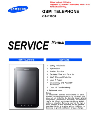
1. GSM TELEPHONE
GT-P1000
1. Safety Precautions
2. Specification
3. Product Function
4. Exploded View and Parts list
5. MAIN Electrical Parts List
6. Level 1 Repair
7. Disassembly and Assembly
Instructions
8. Chart of Troubleshooting
9. Reference data
Notice :
All functionality, features, specifications and other
product information provided in this document inclu
ding, but not limited to, the benefits, design, pricing,
components, performance, availability, and capabiliti
-es of the product are subject to change without
notice or obligation. Samsung reserves the right to
make changes to this document and the product
described herein, at anytime, without obligation on
Samsung to provide notification of such change.
GSM TELEPHONE CONTENTS
2. This Service Manual is a property of Samsung Electronics Co.,Ltd.
Any unauthorized use of Manual can be punished under applicable
International and/or domestic law.
Samsung Electronics Co.,Ltd.
2010. 09. Rev.1.0
ⓒ
Country Web Site
North America service.samsungportal.com
Latin America latin.samsungportal.com
CIS cis.samsungportal.com
Europe europe.samsungportal.com
China china.samsungportal.com
Asia asia.samsungportal.com
Mideast & Africa mea.samsungportal.com
GSPN (Global Service Partner Network)
5. SAMSUNG Proprietary-Contents may change without notice
3. Operation Instruction and Installation
3-1
This Document can not be used without Samsung's authorization
Main Function
• Android OS: Froyo
• HSDPA 7.2Mbps / HSUPA 5.76Mbps
• 3MP AF with LED Flash
• 7.0" WSVGA TFT Full Touch (C-Type)
• A-GPS / BT v3.0 / USB v2.0 / WiFi (802.11 a/b/g/n)
• Recording 480p (D1, 720*480) / Full HD Playback 1080p, DLNA
• Sensors: Accelation, Magnetic, Gyro, Light
• Additional :
- Application store / Voice & Motion UI
- SMS/MMS/Email/Push Email (Exchange ActiveSync)/
Video Messaging Email
- Multi-touch, Multi-task manager
6. SAMSUNG Proprietary-Contents may change without notice
6. Level 1 Repair
6-1
This Document can not be used without Samsung's authorization
6-1. S/W Download
6-1-1. Pre-requisite for S/W Downloading
Downloader Program (Odin3 v1.31.exe)
GT-P1000 Mobile Phone
JIG BOX (GH99-36900A)
RF Test Cable (GH39-00985A)
JIG Cable (GH39-09211A)
Adapter (GH99-38251A)
Data Link Cable
Binary files
Settings
Data Link Cable
7. SAMSUNG Proprietary-Contents may change without notice
Level 1 Repair
6-2
This Document can not be used without Samsung's authorization
6-1-2. S/W Downloader Program
Load the binary download program by executing the
"Odin3 v1.31.exe" Run this file.
1. Option Selection
- Check Re-Partition, Auto Reboot and F. Reset Time, then select PIT File
8. SAMSUNG Proprietary-Contents may change without notice
Level 1 Repair
6-3
This Document can not be used without Samsung's authorization
2. Enter Device into Download Mode
- Enter the device into Download Mode by pressing down on Volume Down button
and Power On button at the same time.
3. Connect the Device to PC via Data Cable.
Make sure ID:COM box highlighted yellow that the device is connected to the PC.
Volume Down Button
Power On Button
9. SAMSUNG Proprietary-Contents may change without notice
Level 1 Repair
6-4
This Document can not be used without Samsung's authorization
4. Start Downloading PIT file by clicking Start Button. Then wait for "Pass" to be
appear on the screen.
5. Click on Reset button, then unselect Re-Partition box. Then select PDA, PHONE
and CSC Files.
Start Button
10. SAMSUNG Proprietary-Contents may change without notice
Level 1 Repair
6-5
This Document can not be used without Samsung's authorization
7. Remove the battery, then enter Device into Download Mode again as in step #3.
then connect to the PC.
8. Start Downloading PDA, PHONE and CSC files by clicking Start Button. Then
wait for "Pass" to be appear on the screen.
9. Once the device boots up, confirm the downloaded version name and etc. :
*#1234#
Full Reset :
*2767*3855#
11. SAMSUNG Proprietary-Contents may change without notice
9. Reference Abbreviate
This Document can not be used without Samsung's authorization
9-1
Reference Abbreviate
― AAC: Advanced Audio Coding.
― AVC : Advanced Video Coding.
― BER : Bit Error Rate
― BPSK: Binary Phase Shift Keying
― CA : Conditional Access
― CDM : Code Division Multiplexing
― C/I : Carrier to Interference
― DMB : Digital Multimedia Broadcasting
― EN : European Standard
― ES : Elementary Stream
― ETSI: European Telecommunications Standards Institute
― MPEG: Moving Picture Experts Group
― PN : Pseudo-random Noise
― PS : Pilot Symbol
― QPSK: Quadrature Phase Shift Keying
― RS : Reed-Solomon
― SI : Service Information
― TDM : Time Division Multiplexing
― TS : Transport Stream
12. SAMSUNG Proprietary-Contents may change without notice
1. Safety Precautions
1-1
This Document can not be used without Samsung's authorization
1-1. Repair Precaution
― Repair in Shield Box, during detailed tuning. Take specially care of tuning or test, because
specipicty of cellular phone is sensitive for surrounding interference(RF noise).
― Be careful to use a kind of magnetic object or tool, because performance of parts is damaged by
the influence of magnetic force.
― Surely use a standard screwdriver when you disassemble this product, otherwise screw will be
worn away.
― Use a thicken twisted wire when you measure level.
A thicken twisted wire has low resistance, therefore error of measurement is few.
― Repair after separate Test Pack and Set because for short danger (for example an overcurrent
and furious flames of parts etc) when you repair board in condition of connecting Test Pack and
tuning on.
― Take specially care of soldering, because Land of PCB is small and weak in heat.
― Surely tune on/off while using AC power plug, because a repair of battery charger is dangerous
when tuning ON/OFF PBA and Connector after disassembling charger.
― Don't use as you pleases after change other material than replacement registered on SEC System.
Otherwise engineer in charge isn't charged with problem that you don't keep this rules.
13. SAMSUNG Proprietary-Contents may change without notice
Safety Precautions
1-2
This Document can not be used without Samsung's authorization
1-2. ESD(Electrostatically Sensitive Devices) Precaution
Several semiconductor may be damaged easily by static electricity. Such parts are called by ESD
(Electrostatically Sensitive Devices), for example IC,BGA chip etc. Read Precaution below.
You can prevent from ESD damage by static electricity.
― Remove static electricity remained your body before you touch semiconductor or parts with
semiconductor. There are ways that you touch an earthed place or wear static electricity prevention
string on wrist.
― Use earthed soldering steel when you connect or disconnect ESD.
― Use soldering removing tool to break static electricity. , otherwise ESD will be damaged by static
electricity.
― Don't unpack until you set up ESD on product. Because most of ESD are packed by box and
aluminum plate to have conductive power,they are prevented from static electricity.
― You must maintain electric contact between ESD and place due to be set up until ESD is
connected completely to the proper place or a circuit board.
14. SAMSUNG Proprietary-Contents may change without notice
4. Exploded View and Parts List
4-1
This Document can not be used without Samsung's authorization
4-1. Cellular phone Exploded View
QLC01
QRE01
QCA02
QAN02
QBA01
QAN03
QMO01
QVK01
QSC01
QCR103
QSP01
QSP02
QCR03
QCA01
QMP01
QCR47
QME16
QVO01
QJK03
QCK01
QJK07
QCR03
QSD01
QRF07
24. SAMSUNG Proprietary-Contents may change without notice
Main Electrical Parts List
5-10
This Document can not be used without Samsung's authorization
Design LOC SEC CODE Description
ZD400 0406-001223 DIODE-TVS
ZD403 0406-001281 DIODE-TVS
ZD407,ZD408,ZD505 0406-001375 DIODE-TVS
ZD502,ZD701 0403-001688 DIODE-ZENER
ZD506,ZD507,ZD508 0406-001375 DIODE-TVS
ZD509,ZD702 0406-001375 DIODE-TVS
ZD510,ZD511 1405-001296 VARISTOR
Please consult the GSPN website (Samsung Portal) for the most recent version of the product's
part list.
25. SAMSUNG Proprietary-Contents may change without notice
7. Level 2 Repair
7-1
This Document can not be used without Samsung's authorization
loosen the 2 points of screw
screw:1.7 *3.5 (Torque 1.3 ± 0.1, star type)
Use diassembly JIG, loosen the hook
Disassembly the FRONT Ass`y from REAR
loosen the screw, and use assembly JIG, disassembly
battery connector. (screw: 1.4 *3 Torque 1.1+-0.1)
7-1. Disassembly and Assembly Instructions
7-1-1. Disassembly
loosen the screw(2 points)
screw code(6001-002656)
screw driver code(2713577900)
1 disassembly FRONT Ass`y2
disassembly the FRONT Ass`y from REAR3 disassembly the battery connector4
26. SAMSUNG Proprietary-Contents may change without notice
7. Level 2 Repair
7-2
This Document can not be used without Samsung's authorization
loosen the screw5 disassembly the connector6
take off the PBA from the FRONT Ass`y7 take off the PBA from the FRONT Ass`y8
loosen the 7 points of screw
screw: 1.4 *3 Torque 1.1+-0.1
disassembly connector. be careful, do not damage connector.
take off the PBA from the FRONT Ass`y take off the PBA from the FRONT Ass`y
27. SAMSUNG Proprietary-Contents may change without notice
7. Level 2 Repair
7-3
This Document can not be used without Samsung's authorization
disassembly the LCD con to con FPCB9
do not damage the FPCB, be careful.
28. SAMSUNG Proprietary-Contents may change without notice
7. Level 2 Repair
7-4
This Document can not be used without Samsung's authorization
7-1-2. Assembly
Assembly bracket, LCD, TSP1 assembly the LCD con to con FPCB2
Place the PBA on the Front Ass`y3 assembly connector4
Use the assembly JIG, attach the TSP attach LCD con to con tape and fix it
Place the PBA on the Front Ass`y
assembly connector and tighten the screw(7 points)
screw: 1.4 *3 Torque 1.1+-0.1
29. SAMSUNG Proprietary-Contents may change without notice
7. Level 2 Repair
7-5
This Document can not be used without Samsung's authorization
assembly the battery connector5 Assembly Front Ass`y and Rear6
Assembly Front Ass`y and Rear7
tighten screw(2points)
screw code(6001-002656)
screw driver code(2713577900)
8
assembly the battery connector and tighten the
serew(screw: 1.4 *3 Torque 1.1+-0.1)
Assembly the Front Ass`y and Rear
check side gap
tighten screw(2points)
screw:1.7 *3.5 (Torque 1.3 ± 0.1, star type)
30. SAMSUNG Proprietary-Contents may change without notice
This Document can not be used without Samsung's authorization
8. Level 3 Repair
8-2
8-1. Block Diagram
AP
SC5C110ABF
CP
PMB9801
I2C
AP_PMIC_SCL
MicroUSB
Switch
FSA9480UCX
I2C
USB_SW_SCL
7" TFT LCD
CODEC
WM8994
I2S
Codec_I2S_CLK
3.5 PI
EAR JACK
BT/WIFI
BCM4329H
BT_PCM
CP_PCM
UART
(BT)
SDIO
(WLAN)
GPS
BCM4751IUB2G UART
SPEAKER
L/R
EAR
MIC
SIM
SOCKET
3M AF
CAMERA
TRANCEIVER
PMB5703
3G PAM
BAND1
3G PAM
BAND2
2G PAM +
FEM
TQM6M9014
3G LNA
BGA735N16
Saw Filter
D1056
3G PAM
BAND8
RGB 2G/3G RX
2G TX
3G Tx/Rx
Band1
3G Tx/Rx
Band2
3G Tx/Rx
Band8
3G Rx
Band1
3G Tx
Band1
3G Rx Band8
/ 2G GSM
3G Rx Band2
/ 2G PCS
3G Tx
Band8
3G Tx
Band2
2G/3G
Tx/Rx
1.3M FF
CAMERAI2C
CAM_SCL_2.8V
Main TSP
I2C
TOUCH_SCL_2.8V
I2C
AP_SCL
16G
iNand
Fuel gauge
MAX17042G-TI2C
FUEL_AP_SCL
SD card
2G Rx
PCS
2G Rx
GSM
2G/3G RX
VIBTONE
ISA1000
Linear
MOTOR PWM
VIBTONE_PWM
LVSD
Transmitter
Accelation
Sensor
BMA023
BH1721FVC
I2C
AP_SCL_2.8V
MMC
T_FLASH_CLK
SIM_CLK
MHL
I2C
AP_HDMI_SCL
MMC
NAND_CLK
Charger IC
SMB136SET
CHARGER_SCL_2.8V
Touch Key
LED
CAM Flash
I2C
AP_I2C_SCL_2.8V
CMC623
Magnetic
Sensor
AK8973B
Gyro Sensor
K3GTR
AP PMIC
MAX8998
31. SAMSUNG Proprietary-Contents may change without notice
Level 3 Repair
8-2
This Document can not be used without Samsung's authorization
8-2. PCB Diagrams
8-2-1. Top
32. SAMSUNG Proprietary-Contents may change without notice
Level 3 Repair
8-3
This Document can not be used without Samsung's authorization
8-2-2. Bottom
33. SAMSUNG Proprietary-Contents may change without notice
Level 3 Repair
8-4
This Document can not be used without Samsung's authorization
8-3. Flow Chart of Troubleshooting
Equipments
Oscilloscope Digital Multimeter
Power Supply + driver, Tweezer
34. SAMSUNG Proprietary-Contents may change without notice
Level 3 Repair
8-5
This Document can not be used without Samsung's authorization
8-3-1. Power On
Check the Battery Voltage
is more than 3.6V
' Power On ' does not work
Change the Battery
(Battery power is low)
END
No
Yes
Check U700(PMIC) and Power
on voltage(C719>1.2V, C720>1.
2V, C721>1.8V, C723>1.2V,
C730>2.8V)
Change the problem point
(short, open, crack, etc.)
And if PMIC has problem, change U700
No
Yes
Check the Clock at
OSC700(C740) that frequency
is 32K
Check the clock generation circuit related to OSC700
(short, open, crack, etc.)
if OSC700 has problem, change OSC700
No
Yes
Yes
Check "Power on" by power
cable with jig-on
Check the switch circuit,
FET gate voltage, FET voltage
(if FET has some problem, it is to be replaced)
check the initial operation
Yes
No
Yes
35. SAMSUNG Proprietary-Contents may change without notice
Level 3 Repair
8-6
This Document can not be used without Samsung's authorization
VOUT_CHARGER
9
D
G
4
1
S
S
2
3
S
TR704
5
D
D
6
7
D
D
8
R779
C768
D1 6
3 D2
2 G1 5
G2
S11
4S2
U705
C794
C789
R778
3
5
6
D
D
7
8
D
D
9
4
G
S
1
2
S
S
V_BATTERY
TR703
D
C783
C767
R777
IF_CON_SENSE
C740
OSC700
21
C718
0.75V~1.5V UP TO 1200mA
0.75V~1.5V UP TO 1200mA
0.8V~2.3V UP TO 900mA
LDO2,3,10,17
1.6V~3.6V UP TO 1000mA
3.0V~3.6V UP TO 150mA
0.95V~1.3V U P TO 10mA
1.6V~3.3V UP TO 300mA
0.8V~3.3V UP TO 150mA
LDO9(2.8V)
1.6V~3.6V UP TO 150mA
LDO4,5,7
1.6V~3.6V UP TO 150mA
1.6V~3.6V UP TO 300mA
2.8V~3.1V UP TO 450mA
1.6V~3.3V UP TO 300mA
0.95V~1.3V UP TO 10mA
1.6V~3.3V UP TO 300mA
0.8V~3.3V UP TO 150mA
1.6V~3.6V UP TO 300mA
0.8V~3.3V UP TO 150mA
BUCK2
1.6V~3.6V UP TO 150mA
1.6V~3.6V UP TO 1000mA
LDO11,12,13
LDO6,8,9
BUCK1
BUCK4
1.6V~3.6V UP TO 300mA
1.2V~3.3V UP TO 300mA
0.75V~1.5V UP TO 1200mA
LDO6(2.6V)
C110_1.2GHz_VINT_1.15V
1.2V~3.3V UP TO 300mA
1.2V~3.3V UP TO 300mA
BUCK3
0.8V~1.3V UP TO 50mA
1.2V~3.3V UP TO 300mA
1.6V~3.6V UP TO 300mA
1.6V~3.6V UP TO 150mA
2.8V~3.1V UP TO 450mA
C110_1.2GHz_VARM_1.3V
0.8V~3.3V UP TO 150mA
1.6V~3.6V UP TO 150mA
1.6V~3.3V UP TO 300mA
0.75V~1.5V U P TO 1200mA
1.6V~3.6V UP TO 150mA
0.8V~1.3V UP TO 10mA
0.8V~1.3V UP TO 50mA
LDO14,15,16
0.8V~1.3V UP TO 10mA
3.0V~3.6V UP TO 150mA
VADC_3.3V_C110
VINT_1.2V_C110
VARM_1.2V_C110
VCC_1.8V_PDA
VINT_1.2V_C110
MIPI_1.1V_C110
VRTC_3.0V_C110
VUSB_1.1V_C110
CAM_CIF_1.5V
R782
LVDS_VDD3.3V
VDAC_3.3V_C110
V_BAT
V_BAT
C719
R707
R781
C729
VTF_2.8V
CAM_IO_2.8V
K4
BATT
K5
DCIN
K6
LDO7
K7
IN5
K8
IN5
K9
J6
NC12
J7
NC11
J8
CS1
J9
PGND3
K1
LDO4
K10
IN4
K2
LX4
K3
PGND4
H8
IN8
H9
LX3
J1
LDO5
J10
LX3
J2
LX4
J3
PGND4
J4
BATT
J5
DCIN
H1
LDO6
H10
IN3
H2
BUCK4
H3
SAFEOUT1
H4
SAFEOUT2
H5
DETBAT
H6
COM12
H7
COM11
G2
BUCK3
G3
VL
G4
_ONO
G5
VICHG
G6
NO12
G7
NO11
G8
IN8
G9
IN3
F4
_IRQ
F5
BATTMON
F6
NC22
F7
NC21
F8
CS2
F9
PGND2
G1
LDO8
G10
PGND2
E6
COM22
E7
COM21
E8
VLSW2
E9
LX2
F1
LDO9
F10
LX2
F2
LX2
F3
_MR
D8
IN6
D9
IN2
E1
LDO11
E10
IN2
E2
BUCK2
E3
JIGON
E4
_RSO
E5
PWREN
D1
LDO12
D10
PGND1
D2
SET1
D3
SET2
D4
SET3
D5
PWRHOLD
D6
NO22
D7
NO21
C2
PWRON
C3
SDA
C4
SCL
C5
SRAD
C6
LDO10
C7
LDO3
C8
IN6
C9
PGND1
B4
AGND2
B5
VCOIN
B6
IN7
B7
LDO2
B8
IN9
B9
LX1
C1
LDO13
C10
BUCK1
A6
IN7
A7
LDO15
A8
REFBP
A9
LX1
B1
LDO17
B10
LX1
B2
32KHZCP
B3
32KHZAP
1
NC
2
IN1
A1
LDO16
A10
IN1
A2
XOUT
A3
XIN
A4
AGND1
A5
LDO14
VTF_2.8V
U700
NC
L701
L703
C717
R705
C709
C738C735C732 C734C723
C740
C731C724
C715
VUSB_3.3V_C110
VCC_2.8V_PDA
CAM_A_2.8V
V_BAT
C711
R708
C739
3
1
2
R780
D900
C703
VCC_1.8V_PDA
VPLL_1.2V_C110
C706
C702
C728C727
C708 C712
C726
C700
C730
VUSB_5V
C725 C737C736 C721C733
OSC700
21
C718
C720
R750
L702
R704 R706
VUSB_5V
C716
CAM_AF_3.0V
C704
C701
C710C705
VCC_2.8V_PDA
VALIVE_1.2V_C110
MOTOR_3.0V
VARM_1.2V_C110
CAM_3M_1.2V
AP_N_RST_IN
nPOWER
AP_PMIC_IRQ
USB_VBUS_AP
USB_VBUS_CP
IF_CON_SENSE
IF_TXD
IF_RXD
CP_TXD_2.8V
CP_RXD_2.8V
AP_TXD
AP_RXD
UART_SEL
GPIO_nRST
BUCK_1_EN_A
BUCK_1_EN_B
BUCK_2_EN
32KHZ_AP
AP_PMIC_SDA
AP_PMIC_SCL
AP_PMIC_EN
PWRON
AP_PS_HOLD
36. SAMSUNG Proprietary-Contents may change without notice
Level 3 Repair
8-7
This Document can not be used without Samsung's authorization
8-3-2. Initial
The pin #A3, B3 of U301 = swing
property 1.8V and 0V? The pin
A1, B1 of U301 = swing property
2.8V and 0V?
Initial Failure
Check U301 and U601 and related parts
(short, crack, etc.)
END
No
Yes
AP_PS_HOLD(U700_pin #D6)
and AP_N_RST_IN(R706) = "low
-> high"?
Yes
Check U700(crack, open, etc.)
(if U700 has some problem, it is to be replaced)
Yes
No
There is 32.768KHz wave forms
at OSC300(C338) and
OSC700(C740)
Replace OSC 300 and OSC700
R339 >= 1.8V? Check U601 and related parts(short, crack, etc.)
(if U601 has some problem, it is to be replaced)
Replace OSC600 and OSC100
There are 24MHz wave forms at
OSC600(C621) and 26MHz wave
forms at OSC100(C128)
LCD display OK?
Sound is OK?
Check the LCD part(short, crack, etc.)
Check the Audio Part(short, crack, etc.)
No
No
No
No
No
Yes
Yes
Yes
Yes
Yes
38. SAMSUNG Proprietary-Contents may change without notice
Level 3 Repair
8-9
This Document can not be used without Samsung's authorization
8-3-3. Charging Part
Check IFC500 pin #7(or #8)
whether voltage reading is
greater than 5V and current
reading is greater than 1.16A
Abnormal charging part
END
No
Yes
Check U518 pin #6 or #7
whether voltage reading is
greater than 5V
No
Yes
Check U702 output pin C773
whether voltage reading is
greater than 4.2V
No
Yes
Check the TA and the DLC
(TA or DLC may not be connected properly)
Check U518 chip(crack, open, etc.)
(if U518 has some problem, it is to be replaced)
Check U702 chip(crack, open, etc.)
(if U702 has some problem, it is to be replaced)
Yes
Check battery voltage is
change when TA is connected
Check U702 output pin C793
whether voltage is change
when TA is connected
Check U501 output pin C503
whether voltage reading is
greater than 5V
Check U702 chip(crack, open, etc.)
(if U702 has some problem, it is to be replaced)
Check U702 chip(crack, open, etc.)
(if U702 has some problem, it is to be replaced)
Check U501 chip(crack, open, etc.)
(if U501 has some problem, it is to be replaced)
Yes
Yes
Yes
No
No
No
40. SAMSUNG Proprietary-Contents may change without notice
Level 3 Repair
8-11
This Document can not be used without Samsung's authorization
8-3-4. Sim Part
Check the Voltage of SIM
(R345 : 2.8V, R311 : 2.8V)
Insert SIM card
Check the Pin Soldering
of SIM300
Yes
Yes
Yes
No
END
Check the detection & No.
(It will be rebooting) 2.8V)
Resoldering and recheck
Change to the new SIM card
Check the voltage from PMIC and CP.
Unless power, Change the PBA
Yes
No
No
C326
C327
NC3 NC 4
NC 5
6NC
NC7
8NC
NC9
C3 C3
C4C4
C5C5
C6 C6C7C7
C8 C8
NC1
2 NC
SIM300
C1 C1
C2C2
VCC_2.8V_PDA
R346
C323 C328
CP_VSIM
R311
R345
SIM_RSTSIM_IO
SIM_DETECTSIM_IO
SIM_RSTSIM_CLK
41. SAMSUNG Proprietary-Contents may change without notice
Level 3 Repair
8-12
This Document can not be used without Samsung's authorization
8-3-5. Microphone Part
Check the MIC or MIC_FPCB
(short, crack, etc)
Check component soldering
statuses of C434, C435
Change MIC or MIC_FPCB
Resolder or replace C434, C435
END
No
Yes
Yes
Yes
No
Check main microphone function
in voice call receiver mode
Check the voltage at
C407 = 2.1V
No
Resolder or replace U402
Yes
43. SAMSUNG Proprietary-Contents may change without notice
Level 3 Repair
8-14
This Document can not be used without Samsung's authorization
8-3-6. Speaker Part
Check the signals on
L410, L411, L412, L413
Check speaker function.
Play MP3 with maximum volume level.
No
Resolder or replace UCD400
END
Yes
Yes
Replace the speaker
module
Yes
44. SAMSUNG Proprietary-Contents may change without notice
Level 3 Repair
8-15
This Document can not be used without Samsung's authorization
C404C403
SPK400
C421
C402
C422
C401
D402
C420
D404
D401
D403
SPK401
C419
L411
L410
L413
L412
SPK_OUTR_P
SPK_OUTR_N
SPK_OUTL_N
SPK_OUTL_P
45. SAMSUNG Proprietary-Contents may change without notice
Level 3 Repair
8-16
This Document can not be used without Samsung's authorization
8-3-7. BT/WIFI
BT/WiFi is not working
Check BT or WiFi function
ON
No
Enable BT or WiFi Function
Yes
END
Check the Voltage on C220 =
2.8V
No Check AP PMIC(700)(crack, open, etc.)
(if PMIC has some problem, it is to be
replaced)
Yes
Check 26MHz Clock at R208
No Check OSC201(crack, open, etc.)
(if OSC201 has some problem, it is to be
replaced)
Yes
Check the Voltage on L213 =
1.5V
No
Resolder or change L213
Yes
Check the Status of
C296, ANT202
No
Resolder or Replace C296, ANT202
Yes
Resolder or Replace U202
Yes
Yes
47. SAMSUNG Proprietary-Contents may change without notice
Level 3 Repair
8-18
This Document can not be used without Samsung's authorization
8-3-8. LCD
LCD is still off after PWR ON
Yes
No
Reconnect the HDC801
Check the connection of
HDC801
Yes
END
No
Resolder L804
Check the R845 short and
High(1.8V)
Yes
No Check the PMU(crack, open, etc.)
(if PMU has some problem, it is to be
replaced)
Check the soldering status of
L804
Yes
Check C808 = 1.8V,
C806 = 3.3V
Yes
Check the signal of
CMC_B(0), CMC_G(3),
CMC_R(7)
Check C837 = 3.3V,
C832 = 1.2V,
C821 = 1.8V
Replace LCD
Module
Yes
Yes
Yes
No
No
Resolder R845 and reinstall binary
3.3V resolder or change U807
1.2V resolder or change U804
1.8V check the PMU
No Check the freq of
OSC800(19.2MHz)
Replace or resolder U808
Yes
Replace or resolder
OSC800
No
49. SAMSUNG Proprietary-Contents may change without notice
Level 3 Repair
8-20
This Document can not be used without Samsung's authorization
8-3-9. TSP
Touch Screen does not work
Yes
No
Reconnect the HDC801Check LCD Connector on
Main PBA
Yes
END
No
Reconnect the HDC800Check the TSP Connector on
LCD Module
Yes
No
Resolder or Replace U801
U801 Pin7 = 2.8V(C813)
and Pin8 = 2.8V(C812)
Yes
Replace LCD Module
Yes
Check the I2C signal of
Sensor IC(R805, R806)
Yes
Resolder R805, R806 or Replace U802
No
51. SAMSUNG Proprietary-Contents may change without notice
Level 3 Repair
8-22
This Document can not be used without Samsung's authorization
8-3-10. 3M CAM
Yes
Check the Camera
connector on Main PBA Reconnect the HDC802, HDC803
No
Check the voltage
C825 = 2.8V,
C824 = 1.2V
C826 = 2.8V
Yes
Check the HDC802, HDC803
Replace U700 or change PBA
No
Yes
Check U601 related to 24MHz
No
Check R819 is 24MHz
Yes
END
Replace the camera module
"Camera" function does not work
Check R818 is 54MHz
No
Check the Pin 21 of HDC802
(Whether the Pin is Short with Pin 19, 20 or not)
Yes
Yes
53. SAMSUNG Proprietary-Contents may change without notice
Level 3 Repair
8-24
This Document can not be used without Samsung's authorization
8-3-11. 1.3M CAM
Yes
Check the Camera
connector on Main PBA Reconnect the HDC802, HDC803
No
Check the voltage
C828 = 2.8V,
C829 = 1.5V
C830 = 2.8V
Yes
Check the HDC802, HDC803
Replace U700 or change PBA
No
Yes
Check U601 related to 12MHz
No
Check R819 is 12MHz
Yes
END
Replace the camera module
"Camera" function does not work
Check R818 is 24MHz
No
Check the Pin 21 of HDC802
(Whether the Pin is Short with Pin 19, 20 or not)
Yes
Yes
55. SAMSUNG Proprietary-Contents may change without notice
Level 3 Repair
8-26
This Document can not be used without Samsung's authorization
Check C117 -65dBm ?
8-3-12. GSM850 RX
NORMAL CONDITION
catch the channel?
Check the voltage at
{R100 = VOUT_CHARGER ?}
& {C110, C343 = 2.85V ?}
& {C111,C112,C337 = 1.8V?}
& {C102,C342 = 2.85V ?}
Check the Voltage at
C136 =VOUT_CHARGER
Check component
soldering status OK at
F100
CHECK soldered
RFS100, L105,C117,C119
Resolder or change
PAM100, C136
Resolder or change
F100
Change U302
Check the freq. at C128
: 26MHz ?
Change or resolder
OSC100
Check C126, L109, C125
-65dBm ?
Resolder or change
C126, L109, C125
GSM850 Receiver is O.K? Change U302
END
NO
YES
NO
NO
YES
NO
YES
NO
YES
NO
YES
NO
YES
NO
Check F100 PIN 8,9
-65dBm
Resolder or change
F100
NO
YES
57. SAMSUNG Proprietary-Contents may change without notice
Level 3 Repair
8-28
This Document can not be used without Samsung's authorization
Check C117 -65dBm ?
8-3-13. GSM1800 RX
NORMAL CONDITION
catch the channel?
Check the voltage at
{R100 = VOUT_CHARGER ?}
& {C110, C343 = 2.85V ?}
& {C111,C112,C337 = 1.8V?}
& {C102,C342 = 2.85V ?}
Check the Voltage at
C136 =VOUT_CHARGER?
Check component
soldering status OK at
F100
CHECK soldered
RFS100,L105,C117,C119
Resolder or change
PAM100, C136
Resolder or change
F100
Change U302
Check the freq. at C128
: 26MHz ?
Change or resolder
OSC100
Check C138, L110
-65dBm ?
Resolder or change
C138, L110
GSM1800 Receiver is O.K? Change U302
END
NO
YES
NO
NO
YES
NO
YES
NO
YES
NO
YES
NO
NO
YES
Check F100 PIN 14, 15
-65dBm
Resolder or change
F100
NO
YES
59. SAMSUNG Proprietary-Contents may change without notice
Level 3 Repair
8-30
This Document can not be used without Samsung's authorization
Check C117 -65dBm ?
8-3-14. WCDMA Band1 RX
CONTINUOUS RX ON
RF INPUT : 10700CH
AMP : -50dBm
NORMAL CONDITION
catch the channel?
Check the Voltage at
C136 =VOUT_CHARGER?
Check component soldering
status OK at PAM103, C115,
L103, L102, C114 ?
CHECK soldered
RFS100, L105, C117, C119
Resolder or change
C136, PAM100
Resolder or change
PAM103, C115,
L103, L102, C114
Change U302
Check the freq. at OSC100
:26MHz ?
Resolder or change
OSC100
PAM100 CHECK
pin7 or L114,C144,C168
-65dBm ?
Resolder or change
PAM100,L114,C144,C168
WCDMA BAND1 Receiver is O.K? Change U302
END
NO
YES
NO
NO
YES
NO
YES
NO
YES
NO
YES
NO
YES
NO
YES
Check component soldering
status OK at
U100, F100 ?
F100 PIN 10, 11 -65dBm
Resolder or change
U100, F100
NO
Check the voltage at
{R100 = VOUT_CHARGER ?}
& {C110, C343 = 2.85V ?}
& {C111,C112,C337 = 1.8V?}
& {C102,C342 = 2.85V ?}
YES
61. SAMSUNG Proprietary-Contents may change without notice
Level 3 Repair
8-32
This Document can not be used without Samsung's authorization
Check C117 -65dBm ?
8-3-15. WCDMA Band2 / GSM1900 RX
CONTINUOUS RX ON
RF INPUT : 9800CH
AMP : -50dBm
NORMAL CONDITION
catch the channel?
Check the Voltage at
C136 =VOUT_CHARGER?
Check component soldering
status OK at PAM102, C100,
L117, C167 ?
CHECK soldered
RFS100, L105, C117, C119
Resolder or change
C136, PAM100
Resolder or change
PAM102, C100, L117, C167
Change U302
Check the freq. at OSC100
:26MHz ?
Change or resolder
OSC100
PAM100 CHECK
pin9 or C127,C145,C143,L111
-65dBm ?
Resolder or change
PAM101, C143, C145, L113
WCDMA BAND2, PCS1900 Receiver is O.K? Change U302
END
NO
YES
NO
NO
YES
NO
YES
NO
YES
NO
YES
NO
YES
NO
YES
Check component soldering
status OK at
U100, F100 ?
F100 PIN 12, 13 -65dBm
Resolder or change
U100, F100
NO
YES
Check the voltage at
{R100 = VOUT_CHARGER ?}
& {C110, C343 = 2.85V ?}
& {C111,C112,C337 = 1.8V?}
& {C102,C342 = 2.85V ?}
63. SAMSUNG Proprietary-Contents may change without notice
Level 3 Repair
8-34
This Document can not be used without Samsung's authorization
Check C117 -65dBm ?
8-3-16. WCDMA Band8 / GSM900 RX
CONTINUOUS RX ON
RF INPUT : 9800CH
AMP : -50dBm
NORMAL CONDITION
catch the channel?
Check the Voltage at
C136 =VOUT_CHARGER?
Check component soldering
status OK at PAM101, C122,
L108, L107, C121 ?
Check C116 -65dBm ?
CHECK soldered
RFS100, L105, C117, C119
Resolder or change
C136, PAM100
Resolder or change
PAM101, C122, L108, L107,
C121, C116
Change U302
Check the freq. at OSC100
:26MHz ?
Change or resolder
OSC100
PAM100 CHECK
pin5 or C142, L112
-65dBm ?
Resolder or change
PAM100, C142, L112
WCDMA BAND8, GSM900 Receiver is O.K? Change U302
END
NO
YES
NO
NO
YES
NO
YES
NO
YES
NO
YES
NO
YES
NO
YES
Check component soldering
status OK at
U100, F100 ?
F100 PIN 6, 7 -65dBm
Resolder or change
U100, F100
NO
YES
Check the voltage at
{R100 = VOUT_CHARGER ?}
& {C110, C343 = 2.85V ?}
& {C111,C112,C337 = 1.8V?}
& {C102,C342 = 2.85V ?}
65. SAMSUNG Proprietary-Contents may change without notice
Level 3 Repair
8-36
This Document can not be used without Samsung's authorization
PAM100 PIN1 : About
30dBm ?
8-3-17. GSM850/GSM900 TX
Check the voltage at
{R100 = VOUT_CHARGER ?}
& {C110, C343 = 2.85V ?}
& {C111,C112,C337 = 1.8V?}
& {C102,C342 = 2.85V ?}
Check the Voltage at
C136,C135,C137 =
VOUT_CHARGER?
Check PAM100 pin 25
about 4dBm
CHECK soldered
RFS100,L105,C117,C119,
C187,C120,L116,C165,ANT101
Resolder or change
PAM100, C136, C135, C137
Resolder or change
U101
Change U302
Check the freq. at C128
: 26MHz ?
Change or resolder
OSC100
Check C132 about 2 V
ok?
Resolder or change
U101
GSM850/900 Transmitter is O.K? Change U302
END
NO
YES
NO
YES
NO
YES
NO
YES
NO
YES
NO
YES
NO
CONTINOUS TX ON CONDITION
TX POWER DAC:14500 CODE
APPLIED
GSM850 CH : 190
GSM900 CH : 62
RBW : 100KHz
VBW : 100KHz
SPAN : 10MHz
REF LEV. : 10dBm
ATT. : 20dB
66. SAMSUNG Proprietary-Contents may change without notice
Level 3 Repair
8-37
This Document can not be used without Samsung's authorization
PAM100 PIN1 : About
27dBm ?
8-3-18. DCS/PCS TX
Check the voltage at
{R100 = VOUT_CHARGER ?}
& {C110, C343 = 2.85V ?}
& {C111,C112,C337 = 1.8V?}
& {C102,C342 = 2.85V ?}
Check the Voltage at
C136,C135,C137 =
VOUT_CHARGER?
Check PAM100 pin 14
about 4dBm
CHECK soldered
RFS100,L105,C117,C119,
C187,C120,L116,C165,ANT101
Resolder or change
PAM100, C136, C135, C137
Resolder or change
U101
Change U302
Check the freq. at C128
: 26MHz ?
Change or resolder
OSC100
Check C132 about 1.8 V
ok?
Resolder or change
U101
DCS/PCS Transmitter is O.K? Change U302
END
NO
YES
NO
YES
NO
YES
NO
YES
NO
YES
NO
NO
YES
CONTINOUS TX ON CONDITION
TX POWER DAC:14500 CODE
APPLIED
GSM850 CH : 190
GSM900 CH : 62
RBW : 100KHz
VBW : 100KHz
SPAN : 10MHz
REF LEV. : 10dBm
ATT. : 20dB