
Recommended
More Related Content
What's hot
What's hot (20)
Similar to pioneer_cdj-900_sm.pdf
Similar to pioneer_cdj-900_sm.pdf (20)
Recently uploaded
Recently uploaded (20)
pioneer_cdj-900_sm.pdf
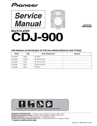
- 1. ORDER NO. PIONEER CORPORATION 4-1, Meguro 1-chome, Meguro-ku, Tokyo 153-8654, Japan PIONEER ELECTRONICS (USA) INC. P.O. Box 1760, Long Beach, CA 90801-1760, U.S.A. PIONEER EUROPE NV Haven 1087, Keetberglaan 1, 9120 Melsele, Belgium PIONEER ELECTRONICS ASIACENTRE PTE. LTD. 253 Alexandra Road, #04-01, Singapore 159936 PIONEER CORPORATION 2009 2009 Printed in Japan CDJ-900 RRV4000 MULTI PLAYER CDJ-900 THIS MANUAL IS APPLICABLE TO THE FOLLOWING MODEL(S) AND TYPE(S). Model Type Power Requirement Remarks CDJ-900 CUXJ AC 120 V CDJ-900 SYXJ8 AC 220 V to 240 V CDJ-900 FLXJ AC 110 V to 240 V CDJ-900 KXJ5 AC 220 V to 240 V CDJ-900 AXJ5 AC 220 V For details, refer to "Important Check Points for good servicing". K-IZE OCT.
- 2. 2 CDJ-900 1 2 3 4 A B C D E F 1 2 3 4 SAFETY INFORMATION WARNING This product may contain a chemical known to the State of California to cause cancer, or birth defects or other reproductive harm. Health & Safety Code Section 25249.6 - Proposition 65 This service manual is intended for qualified service technicians ; it is not meant for the casual do-it- yourselfer. Qualified technicians have the necessary test equipment and tools, and have been trained to properly and safely repair complex products such as those covered by this manual. Improperly performed repairs can adversely affect the safety and reliability of the product and may void the warranty. If you are not qualified to perform the repair of this product properly and safely, you should not risk trying to do so and refer the repair to a qualified service technician. Additional Laser Caution 1. Laser Interlock Mechanism The position of the switch (S8902) for detecting loading completion is detected by the system microprocessor, and the design prevents laser diode oscillation when the switch is not in LPS1 terminal side (when the mechanism is not clamped and LPS1 signal is high level.) Thus, the interlock will no longer function if the switch is deliberately set to LPS1 terminal side. ( if LPS1 signal is low level ). In the test mode ∗ the interlock mechanism will not function. Laser diode oscillation will continue, if pin 5 of AN22022A (IC7004) on the SRV Assy is connected to GND, or else the terminals of Q7002 are shorted to each other (fault condition). 2. When the cover is opened, close viewing of the objective lens with the naked eye will cause exposure to a Class 1 laser beam. IMPORTANT THIS PIONEER APPARATUS CONTAINS LASER OF CLASS 1. SERVICING OPERATION OF THE APPARATUS SHOULD BE DONE BY A SPECIALLY INSTRUCTED PERSON. For CD Wave length (typ) : 790 nm Operation output : 4 mW CW, Class 1 Maximum output : Class 1 (Under fault condition) Laser Pickup specifications and Laser characteristics
- 3. 3 CDJ-900 5 6 7 8 5 6 7 8 A B C D E F LABEL CHECK (Printed on the bottom plate) CUXJ (Printed on the bottom plate) FLXJ (Printed on the bottom plate) SYXJ8 (Printed on the bottom plate) KXJ5 (Printed on the bottom plate) AXJ5
- 4. 4 CDJ-900 1 2 3 4 A B C D E F 1 2 3 4 [Important Check Points for Good Servicing] In this manual, procedures that must be performed during repairs are marked with the below symbol. Please be sure to confirm and follow these procedures. 1.Product safety Please conform to product regulations (such as safety and radiation regulations), and maintain a safe servicing environment by following the safety instructions described in this manual. 1 Use specified parts for repair. Use genuine parts. Be sure to use important parts for safety. 2 Do not perform modifications without proper instructions. Please follow the specified safety methods when modification(addition/change of parts) is required due to interferences such as radio/TV interference and foreign noise. 3 Make sure the soldering of repaired locations is properly performed. When you solder while repairing, please be sure that there are no cold solder and other debris. Soldering should be finished with the proper quantity.(Refer to the example) 4 Make sure the screws are tightly fastened. Please be sure that all screws are fastened, and that there are no loose screws. 5 Make sure each connectors are correctly inserted. Please be sure that all connectors are inserted, and that there are no imperfect insertion. 6 Make sure the wiring cables are set to their original state. Please replace the wiring and cables to the original state after repairs. In addition, be sure that there are no pinched wires, etc. 7 Make sure screws and soldering scraps do not remain inside the product. Please check that neither solder debris nor screws remain inside the product. 8 There should be no semi-broken wires, scratches, melting, etc.on the coating of the power cord. Damaged power cords may lead to fire accidents, so please be sure that there are no damages. If you find a damaged power cord, please exchange it with a suitable one. 9 There should be no spark traces or similar marks on the power plug. When spark traces or similar marks are found on the power supply plug, please check the connection and advise on secure connections and suitable usage. Please exchange the power cord if necessary. a Safe environment should be secured during servicing. When you perform repairs, please pay attention to static electricity, furniture, household articles, etc.in order to prevent injuries. Please pay attention to your surroundings and repair safely. 2.Adjustments To keep the original performance of the products, optimum adjustments and confirmation of characteristics within specification. Adjustments should be performed in accordance with the procedures/instructions described in this manual. 4.Cleaning For parts that require cleaning, such as optical pickups, tape deck heads, lenses and mirrors used in projection monitors, proper cleaning should be performed to restore their performances. 3.Lubricants, Glues, and Replacement parts Use grease and adhesives that are equal to the specified substance. Make sure the proper amount is applied. 5.Shipping mode and Shipping screws To protect products from damages or failures during transit, the shipping mode should be set or the shipping screws should be installed before shipment. Please be sure to follow this method especially if it is specified in this manual.
- 5. 5 CDJ-900 5 6 7 8 5 6 7 8 A B C D E F CONTENTS SAFETY INFORMATION.......................................................................................................................................................... 2 1. SERVICE PRECAUTIONS.................................................................................................................................................... 6 1.1 NOTES ON SOLDERING............................................................................................................................................... 6 1.2 NOTES ON FLASH ROM ............................................................................................................................................... 6 1.3 NOTES ON PANEL CPU AND GUI CPU........................................................................................................................ 6 1.4 NOTES ON LINK CONNECTOR .................................................................................................................................... 7 1.5 REPAIR OF THE JACB ASSY........................................................................................................................................ 7 2. SPECIFICATIONS................................................................................................................................................................. 8 2.1 SPECIFICATIONS .......................................................................................................................................................... 8 2.2 DISCS / FILES PLAYABLE ............................................................................................................................................. 9 2.3 PANEL FACILITIES....................................................................................................................................................... 11 3. BASIC ITEMS FOR SERVICE ............................................................................................................................................ 14 3.1 CHECK POINTS AFTER SERVICING ......................................................................................................................... 14 3.2 PCB LOCATIONS......................................................................................................................................................... 15 3.3 JIGS LIST ..................................................................................................................................................................... 17 4. BLOCK DIAGRAM .............................................................................................................................................................. 18 4.1 OVERALL WIRING DIAGRAM ..................................................................................................................................... 18 4.2 SIGNAL BLOCK DIAGRAM.......................................................................................................................................... 20 4.3 POWER SUPPLY BLOCK DIAGRAM........................................................................................................................... 22 5. DIAGNOSIS ........................................................................................................................................................................ 24 5.1 POWER ON SEQUENCE............................................................................................................................................. 24 5.2 TROUBLESHOOTING.................................................................................................................................................. 26 5.3 FAILURE JUDGEMENT OF THE PICKUP ASSY ........................................................................................................ 39 5.4 CONNECTION CHECK WITH THE PC........................................................................................................................ 40 6. SERVICE MODE................................................................................................................................................................. 41 6.1 OUTLINE OF THE SERVICE MODE............................................................................................................................ 41 6.2 ABOUT THE DEVICE OF CDJ-900.............................................................................................................................. 41 6.3 DETAILS ON SERVICE MODE .................................................................................................................................... 42 7. DISASSEMBLY ................................................................................................................................................................... 55 8. EACH SETTING AND ADJUSTMENT ................................................................................................................................ 66 8.1 JOG DIAL ROTATION LOAD ADJUSTMENT............................................................................................................... 66 8.2 ITEMS FOR WHITCH USERS SETTING IS AVAILABLE............................................................................................. 67 8.3 UPDATING OF THE FIRMWARE AND RECOVERY.................................................................................................... 67 9. EXPLODED VIEWS AND PARTS LIST............................................................................................................................... 68 9.1 PACKING SECTION ..................................................................................................................................................... 68 9.2 EXTERIOR SECTION .................................................................................................................................................. 70 9.3 CONTROL PANEL SECTION....................................................................................................................................... 72 9.4 JOG DIAL SECTION .................................................................................................................................................... 74 9.5 SLOTIN MECHA SECTION.......................................................................................................................................... 76 10. SCHEMATIC DIAGRAM.................................................................................................................................................... 78 10.1 SRV ASSY (1/2).......................................................................................................................................................... 78 10.2 SRV ASSY (2/2) and SLMB ASSY ............................................................................................................................. 80 10.3 MAIN ASSY (1/3)........................................................................................................................................................ 82 10.4 MAIN ASSY (2/3)........................................................................................................................................................ 88 10.5 MAIN ASSY (3/3) and USBA ASSY ........................................................................................................................... 94 10.6 JACB ASSY ................................................................................................................................................................ 96 10.7 DFLB and ENCB ASSYS............................................................................................................................................ 98 10.8 KSWB ASSY............................................................................................................................................................. 100 10.9 SLDB ASSY.............................................................................................................................................................. 102 10.10 BFLB ASSY ............................................................................................................................................................ 104 10.11 MSWB ASSY.......................................................................................................................................................... 106 10.12 JOGB ASSY ........................................................................................................................................................... 107 10.13 JFLB ASSY............................................................................................................................................................. 108 10.14 POWER SUPPLY and ACIN ASSYS ...................................................................................................................... 110 10.15 WAVEFORMS......................................................................................................................................................... 112 11. PCB CONNECTION DIAGRAM ...................................................................................................................................... 116 11.1 SRV and SLMB ASSYS............................................................................................................................................ 116 11.2 MAIN ASSY .............................................................................................................................................................. 120 11.3 USBA and JACKB ASSYS........................................................................................................................................ 124 11.4 DFLB and ENCB ASSYS.......................................................................................................................................... 126 11.5 KSWB and SLDB ASSYS......................................................................................................................................... 130 11.6 BFLB and MSWB ASSYS......................................................................................................................................... 134 11.7 JOGB and JFLB ASSYS........................................................................................................................................... 136 11.8 POWER SUPPLY and ACIN ASSYS ........................................................................................................................ 138 12. PCB PARTS LIST............................................................................................................................................................ 140
- 6. 6 CDJ-900 1 2 3 4 A B C D E F 1 2 3 4 1. SERVICE PRECAUTIONS 1.1 NOTES ON SOLDERING 1.2 NOTES ON FLASH ROM 1.3 NOTES ON PANEL CPU AND GUI CPU • For environmental protection, lead-free solder is used on the printed circuit boards mounted in this unit. Be sure to use lead-free solder and a soldering iron that can meet specifications for use with lead-free solders for repairs accompanied by reworking of soldering. • Compared with conventional eutectic solders, lead-free solders have higher melting points, by approximately 40 ºC. Therefore, for lead-free soldering, the tip temperature of a soldering iron must be set to around 373 ºC in general, although the temperature depends on the heat capacity of the PC board on which reworking is required and the weight of the tip of the soldering iron. Do NOT use a soldering iron whose tip temperature cannot be controlled. Compared with eutectic solders, lead-free solders have higher bond strengths but slower wetting times and higher melting temperatures (hard to melt/easy to harden). The following lead-free solders are available as service parts: • Parts numbers of lead-free solder: GYP1006 1.0 in dia. GYP1007 0.6 in dia. GYP1008 0.3 in dia. NEVER replace the FLASH ROM (IC114) on the MAIN Assy during servicing. If the FLASH ROM is assumed to be defective, replace the whole MAIN Assy. This FLASH ROM contains data that can only be written in at the factory. An IEEE 802.3-based MAC address specific to this unit has been written. After the PANEL CPU (IC8005) or GUI CPU (IC4002) is replaced, update its program. The built-in PANEL CPU and GUI CPU contains a FLASH ROM and will not operate without a program. For updating, proceed as follows: 1. Insert the USB flash memory device that contains the program. 2. While holding the USB STOP key pressed, turn on the unit. Hold the USB STOP key pressed until the “Pioneer” logo disappears. 3. Updating starts.
- 7. 7 CDJ-900 5 6 7 8 5 6 7 8 A B C D E F 1.4 NOTES ON LINK CONNECTOR 1.5 REPAIR OF THE JACB ASSY If the LINK connector (JA1301) is replaced during a repair of the MAIN Assy, detach the ID LABEL (AXW7015) from the old connector then attach it to the new connector. As an IEEE 802.3-based MAC address specific to this unit has been printed on the ID LABEL (AXW7015) be sure to attach it. ID LABEL MAIN Assy When repairing the JACB Assy, note the following: On part of the initial-lot JACB Assy, the DCN1186 (470 ohms, Part description No. 471) is mounted as the resistors (R8820–8823, 8839–8844, 8855, and 8856). In such a case, mount a new DCN1186 during replacement. (See the section 10.6 JACB ASSY.) This applies only to the initial-lot products for the destinations SYXJ8 and FLXJ. For products for other destinations, replace with the DCN1185 (330 ohms, Part description No. 331), as described in the circuit diagram.
- 8. 8 CDJ-900 1 2 3 4 A B C D E F 1 2 3 4 2. SPECIFICATIONS 2.1 SPECIFICATIONS Power requirements.................................... AC 120 V, 60 Hz (CUXJ) AC 220 V to 240 V, 50 Hz/60 Hz (SYXJ8, AXJ5) AC 110 V to 240 V, 50 Hz/60 Hz (FLXJ) AC 220 V, 60 Hz (KXJ5) Power consumption................................................................... 26 W Power consumption (standby).................................................. 0.4 W Main unit weight....................................................................... 3.9 kg External dimensions......305 mm (W) x 115.6 mm (H) x 385 mm (D) Tolerable operating temperature...............................+5 °C to +35 °C Tolerable operating humidity............. 5 % to 85 % (no condensation) Analog audio output (AUDIO OUT L/ R) Output terminal............................................................ RCA terminal Output Level........................................................... 2.0 Vrms (1 kHz) Frequency response.................................................. 4 Hz to 20 kHz S/ N ratio.................................................................................115 dB Total harmonic distortion...................................................... 0.003 % Digital audio output (DIGITAL OUT) Output terminal............................................................ RCA terminal Output type................................................. Coaxial digital (S/ PDIF) Output level............................................................... 0.5 Vp-p (75 Ω) Output format................................................ 44.1 kHz, 24 bit/ 16 bit USB downstream section (USB) Port......................................................................................... Type A Power supply...................................................... 5 V/ 500 mA or less USB upstream section (USB) Port......................................................................................... Type B LAN (PRO DJ LINK) Rating.............................................................................100Base-TX Control output (CONTROL) Port...................................................................................... Mini-jack • The articles concerning free repairs, etc., indicated on the warranty do not apply to the rekordbox music management software. Before installing or using rekordbox, carefully read the articles in Software end user license agreement. • The specifications and design of this product are subject to change without notice.
- 9. 9 CDJ-900 5 6 7 8 5 6 7 8 A B C D E F 2.2 DISCS / FILES PLAYABLE
- 10. 10 CDJ-900 1 2 3 4 A B C D E F 1 2 3 4
- 11. 11 CDJ-900 5 6 7 8 5 6 7 8 A B C D E F 2.3 PANEL FACILITIES
- 12. 12 CDJ-900 1 2 3 4 A B C D E F 1 2 3 4
- 13. 13 CDJ-900 5 6 7 8 5 6 7 8 A B C D E F
- 14. 14 CDJ-900 1 2 3 4 A B C D E F 1 2 3 4 3. BASIC ITEMS FOR SERVICE 3.1 CHECK POINTS AFTER SERVICING Items to be checked after servicing / CDJ To keep the product quality after servicing, confirm recommended check points shown below. No. Procedures Check points 1 2 3 4 5 7 6 Confirm the firmware version on Test Mode. The version of the firmware must be latest. Update firmware to the latest one, if it is not the latest. Confirm whether the customer complain has been solved. If the customer complain occurs with the specific disc, use it for the operation check. The customer complain must not be reappeared. Audio and operations must be normal. Play back a CD. (track search) Audio, Search and operations must be normal. Check the connection of each interface. Play back data contained in the device connected to USB A. Audio, Search and operations must be normal. USB B The device must be recognized by the PC. LINK The PC must be linked. Check output signals while the JOG dial or TEMPO slider is being operated. Audio and operations must be normal. Check the appearance of the product. No scratches or dirt on its appearance after receiving it for service. Check the keys on the unit. Check whether a product can be operated properly by buttons on the product. Item to be checked regarding audio Distortion Noise Volume too low Volume too high Volume fluctuating Sound interrupted See the table below for the items to be checked regarding video and audio. Cleaning Before shipping out the product, be sure to clean the following positions by using the prescribed cleaning tools. Name Position to be cleaned Part No. Remarks Refer to “9.5 SLOTIN MECHA SECTION”. Cleaning liquid Pickup lenses GEM1004 Cleaning paper GED-008 No. Procedures Check points 1 Confirm playback error rates at the innermost and outermost tracks by using the following disc. CD test disc (STD-905) The error rates must be less than 3.0 × 10⁻³. (This procedure can determine if the drive is degraded.) Specific Items to be Checked
- 15. 15 CDJ-900 5 6 7 8 5 6 7 8 A B C D E F 3.2 PCB LOCATIONS 1 B SLMB ASSY A SRV ASSY O ACIN ASSY C MAIN ASSY E JACB ASSY G ENCB ASSY J BFLB ASSY K MSWB ASSY TM ASSY SLOTIN MECHA ASSY H KSWB ASSY POWER SUPPLY ASSY • Bottom view • Bottom view I SLDB ASSY M JFLB ASSY F DFLB ASSY L JOGB ASSY N USBA ASSY D
- 16. 16 CDJ-900 1 2 3 4 A B C D E F 1 2 3 4 LIST OF ASSEMBLIES NOTES: - Parts marked by “NSP” are generally unavailable because they are not in our Master Spare Parts List. - The > mark found on some component parts indicates the importance of the safety factor of the part. Therefore, when replacing, be sure to use parts of identical designation. Mark Symbol and Description CDJ-900 /CUXJ CDJ-900 /SYXJ8 CDJ-900 /FLXJ CDJ-900 /KXJ5 CDJ-900 /AXJ5 NSP 1..DFLA ASSY DWM2361 DWM2361 DWM2361 DWM2361 DWM2361 2..KSWB ASSY DWS1416 DWS1416 DWS1416 DWS1416 DWS1416 NSP 1..JFLA ASSY DWM2362 DWM2356 DWM2356 DWM2356 DWM2356 1..MAIN ASSY DWX3019 DWX3019 DWX3019 DWX3019 DWX3019 1..SRV ASSY DWX3020 DWX3020 DWX3020 DWX3020 DWX3020 1..USBA ASSY DWX3044 DWX3044 DWX3044 DWX3044 DWX3044 2..ACIN ASSY DWR1461 DWR1462 DWR1462 DWR1462 DWR1462 2..MSWB ASSY DWS1415 DWS1415 DWS1415 DWS1415 DWS1415 2..JFLB ASSY DWX3024 DWX3024 DWX3024 DWX3024 DWX3024 2..BFLB ASSY DWX3025 DWX3025 DWX3025 DWX3025 DWX3025 2..JOGB ASSY DWX3026 DWX3026 DWX3026 DWX3026 DWX3026 2..SLDB ASSY DWS1417 DWS1417 DWS1417 DWS1417 DWS1417 2..SLMB ASSY DWS1418 DWS1418 DWS1418 DWS1418 DWS1418 2..DFLB ASSY DWX3021 DWX3021 DWX3021 DWX3021 DWX3021 2..ENCB ASSY DWX3022 DWX3022 DWX3022 DWX3022 DWX3022 2..JACB ASSY DWX3023 DWX3023 DWX3023 DWX3023 DWX3023 > 1..POWER SUPPLY ASSY DWR1463 DWR1463 DWR1463 DWR1463 DWR1463 NSP 1..SLOTIN MECHA ASSY DXA2121 DXA2121 DXA2121 DXA2121 DXA2121 1..TM ASSY 03-S VXX3125 VXX3125 VXX3125 VXX3125 VXX3125
- 17. 17 CDJ-900 5 6 7 8 5 6 7 8 A B C D E F 3.3 JIGS LIST Lubricants and Glues List Name Part No. Remarks Dyfree GEM1036 Refer to “9.5 SLOTIN MECHA SECTION”. Lubricating oil ZLB-HFD1600 Refer to “9.2 EXTERIOR SECTION”, “9.4 JOG DIAL SECTION”. Lubricating oil GYA1001 Refer to “9.4 JOG DIAL SECTION”, “9.5 SLOTIN MECHA SECTION”.
- 18. 18 CDJ-900 1 2 3 4 A B C D E F 1 2 3 4 4. BLOCK DIAGRAM 4.1 OVERALL WIRING DIAGRAM N POWER SUPPLY ASSY (DWR1463) SLOTIN MECHA ASSY (DXA2121) TM ASSY 03-S (DXX3125) D SRV ASSY (DWX3020) C C C 1/3- 3/3 MAIN ASSY (DWX3019) A A A 1/2, 2/2 USBA ASSY (DWX3044) H KS (D E JACB ASSY (DWX3023) B SLMB ASSY (DWS1418) G E (D POWER CABLE ADG7021: CUXJ ADG1154: SYXJ8, FLXJ ADG7097: FLXJ XDG3054: KXJ5 ADG7079: AXJ5 O - Wh - The The - ACIN ASSY (DWR1461: CUXJ) (DWR1462: SYXJ8, FLXJ, KXJ5, AXJ5) CN7005 JA1 CN7301 CN1 JA1101 JA8803 CN7002 CN8901 CN7004 CN2 JA8802 CN7001 CN7003 CN7302 CN1303 CN2001 CN3001 CN501 CN8801 JA8801 CN8501 CN8 CN8001 CN9201 JA9901 CN9901 CN8004 CN1305 POWER CABLE JA1301 XH-XH CABLE FRTN PD TDRV LD65 TRTN FDRV LD78 A VRCOM D VR78 VR65 VREF1 H3- GNDD GNDA INSIDE 7/x6 V+5D H1- RW/XR H2+ F H3+ H2- C GND B GND V+5A EUP_CONT GNDA V+12 V+12 A1 V+12_EUP H1+ A2 A3 E GNDA NC VKN1818-A 1 GNDD 2 ATA_CS1 3 ATA_CS0 4 GNDD 5 ATA_A2 6 ATA_A0 7 GNDD 8 ATA_A1 9 GNDD 10 ATA_IRQ 11 GNDD 12 ATA_DACLK 13 GNDD 14 ATA_RDY 15 GNDD 16 ATA_DIOR 17 GNDD 18 ATA_WR 19 GNDD 20 ATA_DREQ 21 GNDD 22 GNDD 23 ATA_D15 24 ATA_D0 25 ATA_D14 26 ATA_D1 27 ATA_D13 28 ATA_D2 29 ATA_D12 30 ATA_D3 31 ATA_D11 32 ATA_D4 33 ATA_D10 34 ATA_D5 35 ATA_D9 36 ATA_D6 37 ATA_D8 38 ATA_D7 39 GNDD 40 ATA_RESET 1 2 DKN1599-A 1 2 3 4 5 6 B2P3-VH 1 1 2 3 4 5 6 7 8 9 10 11 12 13 14 15 16 17 18 19 20 21 22 23 24 DKN1574-A 1 VBUS 2 D- 3 D+ 4 GNDD DKB1089-A 2 SPDIF 1 GNDD DKN1288-A 1 ST1- 2 ST1+ 3 ST2- 4 ST2+ KM200NA5 1 2 3 4 5 AKM1291-A 1 LO- 2 LO+ 3 GNDD 4 LPS1 5 LPS2 B6B-XH-A 1 2 3 4 5 6 DSA1035-A S1 1 2 VKB1243-A 2 CONT1 3 CONT1 1 CONT2 DKN1445-A 1 2 3 4 5 6 7 8 9 10 11 12 13 14 15 16 17 18 19 20 21 22 23 24 DKN1312-A 1 2 3 4 5 6 7 8 9 10 11 12 AKM1299-A 1 V+12_EUP 2 V+12 3 V+12 4 EUP_CONT 5 GNDD 6 V+3R3 7 V+3R3 8 GNDD 9 V+5 10 GNDD 11 V-11 12 GNDD 13 V+7R2 CKS5075-A 1 2 3 4 5 6 7 8 9 10 11 12 13 14 15 16 17 18 19 20 21 22 23 24 25 26 27 28 29 30 31 32 33 34 35 36 37 38 39 40 VKN1430-A 1 ENV 2 FLCON_CNVSS 3 PNL_SCLK 4 FLCON_BUSY 5 PNL_RXD 6 CLK_REQ 7 PNL_BUSY 8 FLCON_RESET 9 PNL_TXD 10 PNL_CNVSS 11 GNDD 12 PNL_RESET 13 GNDD 14 GNDD 15 V+7R2 16 GNDD 17 V+12 18 V+12_EUP 19 V+12 20 GNDD 21 V+3R3 22 USB_SW 23 EUP_CONT 24 USB_LED 25 CPU_EUP_CONT 26 V+5 AKM1284-A 1 2 3 4 5 6 7 8 9 10 11 12 13 VKN1938-A 1 V+10A 2 ROUT 3 GNDA 4 GNDA 5 LOUT 6 V-10A 7 V+REF2R5 8 MUTE 9 CONT1 10 CONT2 11 GNDD 12 SPDIF KM200NA12 1 2 3 4 5 6 7 8 9 10 11 12 AKB7181-A 5 GNDD 4 GNDD 3 L_OUT 2 GNDD 1 R_OUT KM200NA KM20 9607S-20F 1 USB_LED 2 USB_SW 3 1KEY_SW 4 2KEY_SW 5 4KEY_SW 6 8KEY_SW V+5 52492-2020 15 16 17 18 19 20 DKB1087-A 1 V+5USB 2 D- 3 D+ 4 DGND KM200NA5L 1 2 3 4 GNDD 5 GNDD VKN1257-A 1 2 3 4 5 6 7 8 9 10 11 12 13 14 15 16 17 18 19 20 21 22 23 24 25 26 AKM1276-A 1 V+5USB 2 D- 3 D+ 4 5 PH-PH CABLE DKP3849- L=90mm ZWNN1007G28-9-06A L=60mm (WHITE) PH-PH CABLE PF05PP-B17 L=175mm LOADING MOTOR LO- 03 TM.ASS'Y (VWT1225- /J) SPINDLE MOTOR 04 (VXM1112-) LIVE NEUTRAL DKP3822- L=55mm LIVE NEUTRAL USB CONNECTOR (A TYPE) USB CONNECTOR (B TYPE) VIOLET ETHERNET CONNECTOR FFC DDD1500- SAME FACE L=130mm BLUE L R AUDIO OUT CONTROL DIGITAL OUT 04SD PICK UP ASS'Y R (OWY8036- /XDP/5) *STRIGHT TYPE STEPPING MOTOR (VXM1113-) DC MOTOR (DXM1230-) FFC DDD1450- SAME FACE L=115mm LO+ LO- DKN1576-A ZH-PH CABLE DKP3838- L=70mm DDD1445- FFC L=320mm REVERSE FACE 3 *RIGHT ANGLE FRAME GND CHASSIS GND DE007VF0 L=75mm DKP3831- L=60mm EARTH LEAD UNIT ZWNN1007G28-8-06A L=60mm (GRAY) USB CABLE DDA1040- L=100mm *RIGHT ANGLE LO+ FPC FFC PH-PH CAB PF04PP-Q1 L=175mm FFC DDD1501- SAME FACE L=90mm
- 19. 19 CDJ-900 5 6 7 8 5 6 7 8 A B C D E F F DFLB ASSY (DWX3021) H KSWB ASSY (DWS1416) M JFLB ASSY (DWX3024) L JOGB ASSY (DWX3026) I SLDB ASSY (DWS1417) G ENCB ASSY (DWX3022) K MSWB ASSY (DWS1415) J BFLB ASSY (DWX3025) - When ordering service parts, be sure to refer to "EXPLODED VIEWS and PARTS LIST" or "PCB PARTS LIST". - The > mark found on some component parts indicates the importance of the safety factor of the part. Therefore, when replacing, be sure to use parts of identical designation. - : The power supply is shown with the marked box. CN9402 JH9401 CN8501 CN8005 JH9701 CN4001 JH4001 CN8002 CN8001 CN9201 CN8003 CN9403 CN9501 CN8701 CN8006 CKS1072-A 1 JOG_SW 2 NC 3 GNDD 51048-0400 1 GNDD 2 V+3R3 3 JOG1 4 JOG2 KM200NA4L 1 2 3 4 KM200NA4L 1 GNDD 2 ENC_SW 3 ENC_2 4 ENC_1 51048-0700 1 2 3 4 5 6 7 XKP3022-A 1 2 3 4 5 6 7 8 9 10 GNDD 11 12 13 14 15 16 17 18 19 20 21 22 51048-0700 1 V+12 2 GNDD 3 KEY4 4 BROWS_LED 5 TAG_LIST-LED 6 INFO-LED 7 MENU-LED XKP3022-A 1 CLK_REQ 2 FLCON_CNVSS 3 FLCON_BUSY 4 FLCON_SCLK 5 FLCONL_RXD 6 PNL_TXD2 7 FLCON_RESET 8 D_BK 9 D_LAT 10 N.C.(GNDD) 11 D_SDO 12 KEY3 13 KEY4 14 V+3R3 15 GNDD 16 V+7R2 17 GNDD 18 V+12 19 D_SCLK 20 GNDD 21 GNDD 22 V+54 9607S-20F 1 USB_LED 2 USB_SW 3 1KEY_SW 4 2KEY_SW 5 4KEY_SW 6 8KEY_SW 7 V+5 8 AS_IDCM1 9 AS_IDC4 10 AS_IDC3 11 AS_IDC2 12 AS_IDC1 13 AS_IDCM3 14 AS_IDCM2 15 SHIFT_SW 16 KEY2_B 17 CUE_SW 18 PLAY_SW 19 REV_SW 20 GNDD 52492-2020 1 2 3 4 5 6 7 8 9 10 11 12 13 14 15 16 17 18 19 20 52492-1920 1 JOG2 2 JOG1 3 JOG_SW 4 J_DSO 5 J_SCLK 6 J_LAT 7 J_BK 8 V+3R3 9 GNDD 10 V+7R2 11 GNDD 12 V+33 13 GNDD 14 V+12 15 GNDD 16 V+12 17 GNDD 18 GNDD 19 V+54 XKP3019-A 1 2 3 4 5 6 7 8 9 10 11 12 13 14 15 16 17 18 19 A 52151-0410 1 2 3 4 52492-1320 1 2 3 4 5 6 7 8 9 10 11 12 13 52492-1320 1 GNDS 2 ADIN 3 ADCT 4 V+3R3E 5 MT_LED 6 V+12 7 VINYL_LED 8 V+5 9 KEY0 10 GNDD 11 TCH/REL 12 EJECT_LED 13 EUP_LED SHEET SW (DSX1078-) PH-PH CABLE PF04PP-Q17 L=175mm FFC DDD1449- REVERSE FACE L=142mm FFC DDD1490- SAME FACE L=165mm FFC DDD1501- SAME FACE L=90mm FFC DDD1489- REVERSE FACE L=60mm JUMPER WIRE D20PYY0705E L=50mm JUMPER WIRE D20PYY0405E L=50mm EARTH LEAD UNIT L=70 DDF1032-A
- 20. 20 CDJ-900 1 2 3 4 A B C D E F 1 2 3 4 4.2 SIGNAL BLOCK DIAGRAM A SRV ASSY B SLMB ASSY O ACIN ASSY N POWER SUPPLY ASSY E JACB ASSY C MAIN ASSY D USBA ASSY USB High/Full Speed CPU_TXD2 CPU_RXD2 CPU_SCK2 MII LPS1, LPS2 8bit LO-, LO+ 16bit 16bit 16bit JA8802 CONTROL OUT 32bit JA8803 DIGITAL OUT SPDIF SPDIF_OUT JA8801 32bit R OUT ROUT L OUT LOUT ST1+/-, ST2+/- LOAD FEDRV TEDRV TE FE RFENV Q506 IC7004 FEP SODC IC7008 DRIVER IC7002 IN SW IC7006 FLASH 128kB IC8801 04SD PICK UP ASS'Y R (OWY8036- /XDP/5) SPINDLE MOTOR 04 (VXM1112-) M STEPPING MOTOR (VXM1113-) M DC MOTOR (DXM1230-) CN7002 CN8901 CN7004 CN7001 CN7003 SLOT IN MECHA ASSY (DXM1230) 2 5 2 5 12 12 IC8802 5 7 5 7 IC8803 2 1 6 7 IC3003 DAC 8 11 IC501 DSP I2S SPI A6 IC101 MAIN CPU POWER SUPPLY POWER SUPPLY MAIN SYSTEM BUS ( CS0 : 16bit, CS1,3 : 32bit ) IC1304 ETHER POW 14 18 29 89 111 109 112 67 120 119 46 5 4 175, 176 CN9901 CN1305 CN8801 CN501 CN1303 CN7005 CN7301 CN3 CN2 CN7302 CN3001 JA9901 USB_A (TOP) ATAPI
- 21. 21 CDJ-900 5 6 7 8 5 6 7 8 A B C D E F J BFLB ASSY K MSWB ASSY H KSWB ASSY I SLDB ASSY G ENCB ASSY L JOGB ASSY M JFLB ASSY F DFLB ASSY High/Full Speed CPU_TXD2 ( PNL_TXD ) CPU_RXD2 ( PNL_RXD ) CPU_SCK2 ( PNL_SCLK ) MII 100/10Base-T USB Full Speed 16bit 16bit 16bit JOG_SW 32bit JOG1 JOG2 32bit FLCON_SCLK PNL_TXD2 FLCON_RXD FLCON_RXD PNL_TXD2 FLCON_SCLK ENC_SW ENC_2 ENC_1 JOG2 JOG1 JOG_SW Serial ADCT ADIN PNL_SCLK2 PNL_TXD2 PNL_RXD2 Serial Serial IC501 DSP A6 MAIN SYSTEM BUS ( CS0 : 16bit, CS1,3 : 32bit ) IC505 SDRAM 256MB IC108 SDRAM 256MB IC109 SDRAM 256MB IC114 FLASH 4MB IC1304 ETHER IC1101 USB_B Cntroller POWER SUPPLY IC8005 PANEL CPU V8001 DATA FL IC4002 GUI CPU V4001 BROWSE FL CN2001 CN7302 9 5 3 18 22 24 IC8002 IC8003 SW Buffer 33 32 31 31 32 33 5 6 4 5 6 4 SW LED SW LED POWER SUPPLY IC8010 EUP POWER 2 3 2 3 4 4 ROTARY SEARCH SW LED SLIDER V9401 JOG FL 1 3 4 3 4 3 2 1 SHEET SW (DSX1078-) POWER SUPPLY IC9401 POWER (STEP-UP) 27V/33V/54V 90 91 25 27 6,26 92 SW LED 2 1 2 3 2 3 CN9402 CN9501 JH9401 CN9403 CN8003 CN8005 CN8501 CN8701 CN8006 CN9201 CN8001 JH9701 JH4001 CN4001 CN8002 JA1101 JA1301 LINK (REAR) USB_B (REAR) 17 18 19
- 22. 22 CDJ-900 1 2 3 4 A B C D E F 1 2 3 4 4.3 POWER SUPPLY BLOCK DIAGRAM O ACIN ASSY E JACB ASSY C MAIN ASSY A SRV ASSY D USBA ASSY N POWER SUPPLY ASSY Power supply setup sequence Show the power supply controlling the setup order by a circuit. V+3R3 V+12_EUP V+12 CN7301 CN2 V+5 V+5SW V+12_EUP V+7R2 V+12 V+7R2 V+12_EUP V+5USB V-11 V+5A V+10A V+3R3 V+1R2 V+5D V+7R5 V+12 V+7R5 V+12 V+7R5 V+5 V+3D, V+3A V+1R5D V+5D, V+5A V+3R3 V-11 AC V+12_EUP V+12 V+12_EUP V+12 V+12_EUP V+12 V+12_EUP V+12 V+10A for Audio AMP V+12_EUP for SODC for Spindle,Stepper Loading,Actuator Driver for Driver, Flash SODC V+12 V+5 V+3R3 V+5 V+3R3 V+5 for DAC V+3R3 V+10A V-11 V-11 for FEP, SODC IC7301 D/D_CONV 12V -> 7.5V SI-8005Q IC7302 D/D_CONV 12V -> 5V SI-8005Q IC7303 D/D_CONV 12V -> 3.3V SI-8005Q IC7003 5V_REG 7.5V -> 5V BA00DD0WHFP IC7007 1.5V_REG 5V -> 1.5V PQ1LAX95MSP IC7005 3.3V_REG 5V -> 3.3V MM1478DFBE Q1303 Transistor -11V -> -10V 2SD2662 Q1302 Transistor 12V -> 10V 2SB1698 Q1308 Transistor 10V -> 5V 2SB1698 IC3002 D/D_CONV 12V -> 1.235V SI-8005Q Q3001 FET_SW 5V RTQ040P02 D7311 Schottky diode 7.5V -> 7.2V RB060L-40 P2 0.5A P7302 0.375A P7307 1.25A P7301 1.25A P3 1.25A V+12 V-10A V+5D Charge Pump -12V GND for USB Type A IC1102 High-Side_SW 5V BD2051AFJ CN9901 CN1305 V+5USB V+5USB CN8801 CN501 V-10A V-10A CN2001 V+7R2 CN7302 V+7R2 CN3001 V+7R2 CN1 AC V+12 V+5 V+3R3 V+7R5 V+7R2 V+27 V+54 V+33 V+12EUP V+3R3E V-11 1 2 3 4 5 6 7 for MAIN CPU, DSP, flashROM, SDRAM, USB, Logic & ETHER for MAIN CPU, DSP
- 23. 23 CDJ-900 5 6 7 8 5 6 7 8 A B C D E F L JOGB ASSY K MSWB ASSY M JFLB ASSY I SLDB ASSY J BFLB ASSY H KSWB ASSY F DFLB ASSY V+3R3E V+5 V+12 V+3R3 V+7R2 V+54 V+5 V+12 V+12 V+3R3 V+3R3 V+54 V+7R2 V+3R3 V+5 V+3R3 V+12 V+7R2 V+3R3 V+33 V+5 V+7R2 V+12 V+12 V+12 V+5 V+3R3E V+33 V+27 V+12 EUP V+12_EUP V+3R3 V+5 V+12 V+12 12 5 R3 for LED for Slide Vol V+54 V+54 V+7R2 V+7R2 for Data FL V+54 V+54 V+5 V+5 for LED V+33 V+33 V+7R2 V+7R2 V+3R3 V+3R3 IC8010 D/D_CONV 12V -> 3.3V NJM2392M IC9401 D/D_CONV 12V -> 27V NJM2392M Q9413 FET_SW 12V RTQ040P02 Q9414 FET_SW 7.2V RTQ040P02 P9405 0.5A Charge Pump +27V Charge Pump +27V IC9402+T9401 Timer+Trans 12V -> AC2.7V TLC555IP+DTT1232 P9401 0.5A for JOG FL VFDP2R9 V+12 V+12 P9402 1.5A for PNL_uCON for Brows FL for GUI CPU for LED for Jog Rotate Detect for LED for LED 001 CN8004 V+7R2 R2 CN8006 CN8701 V+3R3E CN8003 CN9403 V+3R3 V+3R3 CN8002 CN4001 V+12 V+12 CN8001 CN9201 V+5 V+5 JH4001 JH9701 V+12 V+12 CN9501 V+3R3 JH9401 V+3R3 V+3R3E V+3R3
- 24. 24 CDJ-900 1 2 3 4 A B C D E F 1 2 3 4 5. DIAGNOSIS 5.1 POWER ON SEQUENCE Main CPU ETHER DSP DAC USB_B CONTROLLER GUI CPU Power on Power on Pin Y22 of Main CPU (IC101) cancels reset at H. Program transfer from FLASH to SDRAM Canceling DSP reset from pin B18 of Main CPU. Pin G2 of DSP (IC501) becomes "H". Canceling GUI CPU reset from pin F3 of Main CPU. Canceling PANEL CPU reset from pin P1 of PANEL CPU. Canceling ETHER reset from pin A18 of Main CPU. Pin 42 of ETHER (IC1304) becomes "H". Canceling USB_B CONTROLLER reset from pin A17 of Main CPU. Pin 46 of USB_B CONTROLLER (IC1101) becomes "H". Canceling ATAPI reset from pin C10 of Main CPU. Pin 173 of SODC (IC7006) becomes "H". Program transfer to DSP Initialization of the built-in peripherals Initialization of the SDRAM Initialization of the SDRAM Initialization of the DSP Initialization of the USB_B Initialization of the ETHER Initialization of the DAC Initialization of the peripheral device Initialization of the Main CPU Pin 12 of GUI CPU (IC4002) cancels reset at H. Initialization of the Data and Browse FL Display a Pioneer logo on the Browse FL Displays Browse FL and Data FL. LED initial lighting Pin 12 of PANEL CPU (IC8003) cancels reset at H. Pin 45 of SODC (IC7006) cancels reset at H. Initialization of the GUI CPU PANEL CPU Power on Initialization of the JOG_FL Initialization of the PANEL CPU SERVO Power on Initialization of the ATAPI Display JOG FL. LED initial lighting. Communication between Main CPU and SERVO Initialization of the SODC Built-in peripherals • USB_A • ETH_MAC • ATAPI • SERIAL Bus Communication between Main CPU and PANEL CPU Communication between Main CPU and GUI CPU Initialization of the loading mechanism The insertion of the disk is possible. Power-on Sequence
- 25. 25 CDJ-900 5 6 7 8 5 6 7 8 A B C D E F Power ON Loading of a disc Stepper moving to a focusing position Spin-up (CAV 2000 rpm) Media distinction with the aid of reflectivity Set a gain by media judgement result, and take in the S-shaped signal. Offset canceling TB adjustment TEPP adjustment T close FB adjustment FG adjustment TOC read CLV servo on Searching for the 1st piece of music LD OFF Cancel the getting into of INSIDE SW Initialization of the loading mechanism Turn ON the LD on the CD side to check for the presence of a disc. Without a disc, an unloading process starts. Offset canceling for the 2nd time LD ON for the 2nd time, and focusing Set up Sequence of Servo Section
- 26. 26 CDJ-900 1 2 3 4 A B C D E F 1 2 3 4 5.2 TROUBLESHOOTING In this section, causes of failure, diagnostics points, and corrective measures can be searched for according to symptoms. Before disassembling this unit, it is recommended to infer a failure point by performing a auto device check/alarm port and referring to the error code. Note: Alarm port is the Test port on the MAIN Assy. (Location is referred to the Schematic diagram and PCB Connection diagram.) For the relationship of each power-supply and signal system, see “4.3 POWER SUPPLY BLOCK DIAGRAM.” If software of the product is updated before performing diagnostics, check that software updating has been performed properly before proceeding to diagnostics. If software updating has not been performed properly, update the software, following the instructions in [7] Firmware update of “6.3 DETAILS ON SERVICE MODE.” Contents [0] Prior Confirmation [1] Failure in Startup [2] Display (DATA FL/BROWS FL/JOG FL/LED) [3] Operations (SW/Volume/JOG) [4] USB (Type A/Type B) [5] LAN [6] AUDIO OUT [7] CONTROL [8] DRIVE Assy [9] EUP Mode [10] SERVICE MODE [11] Error Codes The waveform numbers described in this section correspond to the “10.15 WAVEFORMS.” [0] Prior Confirmation [0-1] Checking in Service Mode [0-2] Checking Cables [1] Failure in Startup [1-1] No power No. Cause Diagnostics Point Item to be Checked Corrective Action Reference 1 — Check the failure points in auto device check / alarm port. See the section describing locations of defects in this manual. 6.SERVICE MODE No. Cause Diagnostics Point Item to be Checked Corrective Action Reference 1 Cables Disconnection, breakage, or loose connection of cables Check that all the cables are securely connected. Check that there is no breakage in the cables. Securely connect the cables. If a cable is broken, replace it. 4.1 OVERALL CONNECTION DIAGRAM 4.3 POWER SUPPLY BLOCK DIAGRAM 4.3 POWER SUPPLY BLOCK DIAGRAM Even after the unit is turned on, no indication is displayed nor can loading by the DRIVE Assy be performed. No. Cause Diagnostics Point Item to be Checked Corrective Action Reference 1 Defective power supply SRV Assy Check V+12. If V+12 is not checked, go to step 2. If V+12 is checked, go to step 3. 2 Defective power supply/Protector breakage SRV Assy Check V+12EUP. Check also if the protector (P7302) is broken. If the protector is broken, replace the protector. If the V+12EUP voltage is not output, the SW power-supply IC may be defective. Replace it. 3 Signal errors SRV Assy Check the EUP_CONT signal. If the signal is “L,” check the output from the SW power-supply IC. If V+12 is not output, the SW power- supply IC may be defective. Replace it. If the signal is “H,” check if the signal logics are the same as those for normal status shown in the table in the rightmost column. If either of the signal logics is not the same, check the mounting status of the IC8001 or IC8008 on the DFLB Assy, which corres- ponds to the wrong signal logic. If it is correctly mounted, then it may be defective. Replace it. Refe to “Signal logic during EUP mode.”
- 27. 27 CDJ-900 5 6 7 8 5 6 7 8 A B C D E F [2-3] The BROWS FL does not light. [2] Display (DATA FL/BROWS FL/JOG FL/LED) [2-1] Any of the DATA, BROWS, and JOG FLs are not lit. [2-2] Neither the DATA nor BROWS FL is lit. [1-2] Startup stops with the “Pioneer” logo displayed on the screen. (See *1.) The DATA FL, BROWS FL and the LEDs (LINK, USB, DISC, BROWS, TAG LIST, INFO, MENU) are controlled by the GUI CPU (IC4002). The JOG FL and the other LEDs are controlled by the PANEL CPU (IC8005). 4.3 POWER SUPPLY BLOCK DIAGRAM 4.3 POWER SUPPLY BLOCK DIAGRAM 6.SERVICE MODE 4 Defective power supply/Protector breakage SRV Assy Check V+7R2, V+5, V+3R3 and check whether protector (P7302) does not break. V+7R2 => P7310 V+3R3 => P7307 Refer to 4.3 POWER SUPPLY BLOCK DIAGRAM. If the protector is broken, replace the protector. Check the mounting statuses of the regulator IC and its peripheral parts for each power supply. If they are properly mounted, then the parts may be defective. Replace them. If startup stops in such a status, the upstream and downstream communications between the MAIN CPU and PANEL CPU/GUI CPU could not be established. All types of driver power to be supplied are produced at the JFLB Assy. No. Cause Diagnostics Point Item to be Checked Corrective Action Reference No. Cause Diagnostics Point Item to be Checked Corrective Action Reference 1 Version upgrade failed. — — Version upgrade of the software for the DRIVE unit may have failed. If upgrading failed, startup stops with the “Pioneer” logo displayed on the screen, and the LED for the USB STOP key flashes repeatedly. See “6. SERVICE MODE.” 6.SERVICE MODE 2 — MAIN Assy Check a failure point at the status check (alarm) port of the MAIN Assy. If there is a point that has been judged as in failure, see “6. SERVICE MODE” in this section. No. Cause Diagnostics Point Item to be Checked Corrective Action Reference 1 Defective power supply BFLB Assy Check the power-supply voltages (V+3R3/V+7R2/V+54) of the FL. If the presence of power is not confirmed, check the mounting statuses of the regulator IC and its peripheral parts for each power supply. If they are properly mounted, then the parts may be defective. Replace them. No. Cause Diagnostics Point Item to be Checked Corrective Action Reference 1 Breakage of protectors JFLB Assy/ SRV Assy Check V+12 and check whether protectors do not break. JFLB Assy => P9402/P9405 SRV Assy => P7310 If the protector is broken, replace the protector. 4.3 POWER SUPPLY BLOCK DIAGRAM 4.3 POWER SUPPLY BLOCK DIAGRAM Driver power to be supplied to the DATA and BROWS FLs is produced at the JFLB Assy. No. Cause Diagnostics Point Item to be Checked Corrective Action Reference 1 Defective power supply JFLB Assy Check supply voltages (V+33/V+54) of the FL. If the presence of power is confirmed, check the connections to these FLs. If the presence of power is not confirmed, check the mounting statuses of the power circuit (IC9401) and its peripheral parts. If there is any problem, correct it. 2 Signal errors BFLB Assy Check the output signal and connection of communication line of BROWS FL in the BFLB Assy. • B_SCLK • B_BK • B_LAT • B_DSO If no signal is output, the GUI CPU (IC4002) port may be damaged. Replace it. If soldering is improper, resolder it. 3 Defective parts of FL If the symptom persists after the above corrections, Replace the BROWS FL. Normal mode EUP mode EUP_CONT L H or open PANEL CPU(IC8005) pin28 H L CPU_EUP_CONT X L Reference: Signal logic during EUP mode X : Not Concerned 10.10 BFLB ASSY
- 28. 28 CDJ-900 1 2 3 4 A B C D E F 1 2 3 4 [2-6] The LED does not light. [2-4] The DATA FL does not light. [2-5] The JOG FL does not light. 10.7 DFLB and ENCB ASSYS 10.10 BFLB ASSY 10.13 JFLB ASSY 10.10 BFLB ASSY — No. Cause Diagnostics Point Item to be Checked Corrective Action Reference 1 Defective power supply DFLB Assy Check the power-supply voltages (V+3R3/ V+7R2/V+33) of the FL. If the presence of power is not confirmed, check the mounting statuses of the regulator IC and its peripheral parts for each power supply. If they are properly mounted, then the parts may be defective. Replace them. 4.3 POWER SUPPLY BLOCK DIAGRAM 2 Signal errors DFLB Assy Check the waveforms and connection of the FL communication line in the DFLB Assy. • D_SCLK • D_BK • D_LAT • D_DSO If no signal is output, the GUI CPU (IC4002) port may be damaged. Replace it. If soldering is improper, resolder it. 3 Defective parts of FL If the symptom persists after the above corrections, Replace the DATA FL. — No. Cause Diagnostics Point Item to be Checked Corrective Action Reference 2 Defective power supply JFLB Assy JFLB Assy Check the power-supply voltages (V+3R3/ VFDP2R9_F1/VFDP2R9_F2/V+27) of the FL. If the presence of power is not confirmed, check the mounting statuses of the regulator IC and its peripheral parts for each power supply. If they are properly mounted, then the parts may be defective. Replace them. 4.3 POWER SUPPLY BLOCK DIAGRAM 3 Signal errors JFLB Assy Check the connection of the FL communi- cation line in the JFLB Assy. • J_SCLK • J_BK • J_LAT • J_DSO If no signal is output, the GUI CPU (IC4002) port may be damaged. Replace it. If soldering is improper, resolder it. 4 Defective parts of FL If the symptom persists after the above corrections, Replace the JOG FL. — 1 Breakage of protectors Check if the protector (P9401) is broken. If the protector is broken, replace the protector. LED (LINK, USB, DISC, BROWS, TAG LIST, INFO and MENU) No. Cause Diagnostics Point Item to be Checked Corrective Action Reference 1 Signal errors BFLB Assy Check that the control signal for the LED in question is output from the GUI CPU (IC4002). If no signal is output, the GUI CPU (IC4002) port may be damaged. Replace it. If soldering is improper, resolder it. - 2 Defective parts of LED BFLB Assy Check that the forward voltage (2.2 - 2.7 V) is present at both ends of the LED. If the forward voltage is not present, then the LED itself is defective. Replace it. - 3 Defective parts of transistor BFLB Assy If the symptom persists after the above corrections, The transistor is defective. Replace it. - LED (except for the USB STOP indicator) on KSWB Assy does not light. No. Cause Diagnostics Point Item to be Checked Corrective Action Reference 1 Breakage of protectors MAIN Assy Check if the protector (P3) is broken. If the protector is broken, replace the protector. - 2 - - The LEDs (except for the USB STOP indica- tor) on the KSWB Assy are lit dynamically in a matrix pattern. Check if the unlit LED belongs to a certain line/column group, referring to the circuit diagrams. If it does not belong to a group, then that LED may be defective. Replace it. If it belongs to a group, then the LED-drive signal for that group is defective. Go to [2]. 10.8 KSWB ASSY (Schematic diagram) 3 Signal errors DFLB Assy Check that the control signal for the LED in question is output from the PANEL CPU (IC8005). If no signal is output, the PANEL CPU (IC8005) port may be damaged. Replace it. If soldering is improper, resolder it. - 4 - - If the symptom persists after the above corrections, The transistor is defective. Replace it. - USB STOP indicator does not light. This LED is controlled by the MAIN CPU (IC101). No. Cause Diagnostics Point Item to be Checked Corrective Action Reference 1 Breakage of protectors MAIN Assy Check if the protector (P3) is broken. If the protector is broken, replace the protector. - 2 Defective parts of LED BFLB Assy Check that the forward voltage (2.2 - 2.7 V) is present at both ends of the LED. If the forward voltage is not present, then the LED itself is defective. Replace it. - 3 Defective connection/ Signal errors MAIN Assy/ DFLB Assy/ KSWB Assy Check the connection of the LED control signal. If the signal is not output even if the connections are properly made, the port on the MAIN CPU (IC101) may be damaged. Replace it. - 4 - - If the symptom persists after the above corrections, The transistor is defective. Replace it. -
- 29. 29 CDJ-900 5 6 7 8 5 6 7 8 A B C D E F 10.7 DFLB and ENCB ASSYS Other LED does not light. No. Cause Diagnostics Point Item to be Checked Corrective Action Reference 1 Breakage of protectors Related point Check the drive voltage of the unlit LED. For the 5-V-driven LEDs, check if the protector (P3) is broken. If the protector is broken, replace the protector. - 2 Signal errors - Check that the signal for the LED in question is output from the PANEL CPU (IC8005). When there is not output signal, check the connec- tion of the PANEL CPU (IC8005). If the connection is OK, the port may be damaged. Replace it. - 3 Defective parts of LED - Check that the forward voltage (2.2 - 2.7 V) is present at both ends of the LED. If the forward voltage is not present, then the LED itself is defective. Replace it. - 4 Defective parts of transistor - If the symptom persists after the above corrections, The transistor is defective. Replace it. - [3] Operations (Keys/variable controls/JOG) As operations of all keys, variable controls, and JOG dial can be checked in Service mode. [3-1] No key functions The PLAY, CUE, AUTO BEAT LOOP, BEAT SELECT, REV, LOOP IN, LOOP OUT, or RELOOP key does not function. No. Cause Diagnostics Point Item to be Checked Corrective Action Reference 1 Loose connection /Defective SW Related point Check if there is loose connection on the signal line from the PANEL CPU (IC8005) up to the SW. If there is no loose connection and if the signal does not become L when the SW is pressed, that SW is defective. Replace it. - 2 Defective PANEL CPU (IC8005) DFLB Assy If the symptom persists after the above corrections, Check the connection of the PANEL CPU (IC8005). If the connection is OK, the port may be damaged. Replace it. - Other keys (except for the USB STOP key) do not function. The signals from other keys are analog and connected to multiple switches. No. Cause Diagnostics Point Item to be Checked Corrective Action Reference 1 Loose connection /Defective SW Related point Check if there is loose connection on the signal line from the PANEL CPU (IC8005) up to the SW. If the SWs connected to the signal line function properly and if the connections are properly made, the SWs may be defective. Replace them. - 2 Defective PANEL CPU (IC8005) DFLB Assy If the symptom persists after the above corrections, Check the connection of the PANEL CPU (IC8005). If the connection is OK, the port may be damaged. Replace it. - The USB STOP key does not function. The USB STOP key is controlled by the MAIN CPU. No. Cause Diagnostics Point Item to be Checked Corrective Action Reference 1 Loose connection /Defective SW KSWB Assy/ MAIN Assy Check if there is loose connection on the signal line from the MAIN CPU (IC101) up to the SW. If there is no loose connection and if the signal does not become L when the SW is pressed, that SW is defective. Replace it. - 2 Defective MAIN CPU (IC101) MAIN Assy If the symptom persists after the above corrections, The MAIN CPU (IC101) is defective. Replace it. - [3-2] Rotary selector not controllable No. Cause Diagnostics Point Item to be Checked Corrective Action Reference 1 Defective rotary selector ENCB Assy Check if the signals from the ENC_1, ENC_2, and ENC_SW signal lines are normal when the rotary selector is turned or pressed. If the signals are not normal, check the connections of the signal lines. If the connections are properly made, the encoder selector may be defective. Replace it. 2 Defective PANEL CPU (IC8005) DFLB Assy If the symptom persists after the above corrections, Check a mounting state of PANEL CPU(IC8005). If the mounting is OK, the PANEL CPU is damaged. Replace it. - [3-3] Variable controls not controllable Tempo slider not controllable No. Cause Diagnostics Point Item to be Checked Corrective Action Reference 1 Loose connection SLDB Assy /DFLB Assy Check if there is loose connection on the signal line from the PANEL CPU (IC8005) to the tempo slider (VR8701). If the connections of signal line are improper, resolder it. - 2 Defective tempo slider SLDB Assy Check the waveforms of signal lines (ADCT/ADIN) . If the voltage of the signal line (ADIN) does not change between 3.3 V and 0 V, the tempo slider (VR8701) may be defective. Replace it. - 3 Defective PANEL CPU (IC8005) DFLB Assy If the symptom persists after the above corrections, Check a mounting state of PANEL CPU(IC8005). If the mounting is OK, the port may be damaged. Replace it. -
- 30. 30 CDJ-900 1 2 3 4 A B C D E F 1 2 3 4 VINYL SPEED ADJUST not controllable No. Cause Diagnostics Point Item to be Checked Corrective Action Reference 1 Loose connection SLDB Assy /DFLB Assy Check if there is loose connection on the signal line from the PANEL CPU (IC8005) to the SPEED ADJUST(VR8702). If the connections of signal line are improper, resolder it. - 2 Defective VOL SLDB Assy Check the waveforms of signal lines (TCH/REL). If the voltage of the signal line (TCH/REL) does not change between 3.3 V and 0 V, the VINYL SPEED ADJUST (VR8702) may be defective. Replace it. - 3 Defective PANEL CPU (IC8005) DFLB Assy If the symptom persists after the above corrections, Check a mounting state of PANEL CPU(IC8005). If the mounting is OK, the port may be damaged. Replace it. - [3-4] Abnormalities regarding the JOG dial After the JOG Assy is disassembled then reassembled, be sure to check that the load value for the JOG dial is within the specified range. Turning of the JOG dial is not detected No. Cause Diagnostics Point Item to be Checked Corrective Action Reference 1 Defective photo interrupter JOGB Assy/ JFLB Assy/ DFLB Assy Check the waveforms of signal lines (JOG1/JOG2). If no waveform can be confirmed, the photo interrupter (PC9501) may be defective. Replace it. - 2 Defective PANEL CPU (IC8005) DFLB Assy If the symptom persists after the above corrections, Check a mounting state of PANEL CPU (IC8005). If the mounting is OK, the port may be damaged. Replace it. - Pressing on the JOG dial cannot be detected. No. Cause Diagnostics Point Item to be Checked Corrective Action Reference 1 Defective SHEET SW JFLB Assy /DFLB Assy Check the waveform of the signal on the signal line (JOG_SW) when the JOG dial is pressed. If the signal on the signal line (JOG_SW) is not set to L when the JOG dial is pressed, the SHEET SW (DSX1078-A) may be defective. Replace it. - 2 Defective PANEL CPU (IC8005) DFLB Assy If the symptom persists after the above corrections, Check a mounting state of PANEL CPU(IC8005). If the mounting is OK, the port may be damaged. Replace it. - Noise is heard when the JOG dial is turned. No. Cause Diagnostics Point Item to be Checked Corrective Action Reference 1 Defective JFLB Assy or gears JOG Assy Check if the JOG FL of the JFLB Assy has been shifted upward from the holder. The JOG FL may interfere with JOG A. Replace the JFLB Assy. - There may be any scratches on the 3 gears or some foreign object between the gears. If there are any scratches, replace the scratched gear with a new one. If there is any foreign object, remove it then replace the gears with new ones. Gears to be replaced: Load gear, Gear A, Gear B - The JOG dial turns too freely. (The load value for the JOG dial is outside the specified range.) No. Cause Diagnostics Point Item to be Checked Corrective Action Reference 1 Improper adjust- ment or assembly of the JOG dial JOG Assy Check that the load value for the JOG dial is within the specified range, referring to “Measuring method” in “8.1 JOG Dial Rotation Load Adjustment.” If it is outside the specified range, adjust the position of the Adjust Plate to change the load value for the JOG dial, referring to “How to Adjust” in “8.1 JOG Dial Rotation Load Adjustment.” 8.1 JOG Dial Rotation Load Adjustment. During the above adjustment, if the upper-limit adjust- ment position of the Adjust Plate is reached, oil may have been spattered on the Adjust Plate. Replace the washer, gear, and cam plate with new ones, then reassemble. - Resistance to turning the JOG dial is too strong. (The load value for the JOG dial is outside the specified range.) No. Cause Diagnostics Point Item to be Checked Corrective Action Reference 1 Improper adjust- ment of the JOG dial or defective washer, gear, or cam plate JOG Assy Check that the load value for the JOG dial is within the specified range, referring to “Measuring method” in “8.1 JOG Dial Rotation Load Adjustment.” If it is outside the specified range, adjust the position of the Adjust Plate to change the load value for the JOG dial, referring to “How to Adjust” in “8.1 JOG Dial Rotation Load Adjustment.” 8.1 JOG Dial Rotation Load Adjustment. During the above adjustment, if the lower-limit adjust- ment position of the Adjust Plate is reached, shavings from the worn-out washer may have increased the friction. Replace the washer, gear, and cam plate with new ones, then reassemble. -
- 31. 31 CDJ-900 5 6 7 8 5 6 7 8 A B C D E F 10.5 MAIN ASSY(3/3), USBA ASSY [4] USB (Type A/Type B) [4-1] No communication via the USB connector (Type A) Check the following, with a USB device connected to the USB A connector. No. Cause Diagnostics Point Item to be Checked Corrective Action Reference 1 Loose connections USBA Assy /MAIN Assy Check the connection of the USB communication line. If connection is improper, resolder it. If connection is proper, go to step [2]. - 2 V+5_USB_HOST _VBUS is defective. MAIN Assy Check V+5_USB of the USB power supply. If V+5_USB cannot be confirmed, check V+5. If the V+5 is OK, then go to [3]. If V+5_USB can be confirmed, go to [4]. - 3 The USB PAWED IC is defective. /Signal errors MAIN Assy Check the CPU_USB_HSTPWREN and CPU_USB_HSTPWRFL signals from the USB POWER HIGHT SIDE SW(IC1102) If the CPU_USB_HSTPWREN signal does not become H, check the connection. If the connection is OK, then the MAIN CPU (IC101) is defective. Replace it. If the CPU_USB_HSTPWRFL signal does not become H, the USB POWER HIGH SIDE SW (IC1102) is in a state of shutdown caused by abnormally high temperature. Check the connection. If the connection is OK, then the port may be damaged. Replace it. 4 Defective MAIN CPU MAIN Assy If the symptom persists after the above corrections, The MAIN CPU (IC101) is defective. Replace it. - [4-2] No communication via the USB connector (Type B) Check the following, with a USB device connected to the USB B connector. No. Cause Diagnostics Point Item to be Checked Corrective Action Reference 1 Loose connections Check the connection of the signal lines (USB_D+/USB_D-). If connection is improper, resolder it. - 2 Defective USB CONTROLLER If the symptom persists after the above corrections, The USB CONTROLLER (IC1101) may be defective. Replace it. - [5] LAN [5-1] No LAN communication Check the following, with a peripheral device connected to the Ethernet connector. No. Cause Diagnostics Point Item to be Checked Corrective Action Reference 1 Loose connections MAIN Assy Check the connection of the periphery circuit of ETHER PHY CHIP (IC1304). Check the connections of the communication line. If connection is improper, resolder it. The ETHER PHY CHIP (IC1304) may be defective. Replace it. If the symptom persists, the MAIN CPU (IC101) may be defective. Replace it. - 2 Defective ETHER PHY CHIP or MAIN CPU MAIN Assy If the symptom persists after the above corrections, -
- 32. 32 CDJ-900 1 2 3 4 A B C D E F 1 2 3 4 10.4 MAIN ASSY(2/3) 10.15 WAVEFORMS L, M 10.1 SRV ASSY (1/2) 10.15 WAVE- FORMS 2, 3 10.4 MAIN ASSY(2/3) [6] AUDIO OUT [6-1] No sound The analog audio signal is not output. No. Cause Diagnostics Point Item to be Checked Corrective Action Reference 1 Defective power supply MAIN Assy /JACB Assy Check the voltages for audio (V+10A/V-10A/ REF2R5). Check also if the protector (P2) is broken. If the protector is broken, replace the protector. • If V+10A is not output, check the mounting statuses of Q1302 and Q1304. If there is any problem, correct it. • If V-10A is not output, check the mounting statuses of Q1303 and Q1305. If there is any problem, correct it. • If VREF2R5 is not output, go to [3]. - 2 Loose connections MAIN Assy /JACB Assy Check the connection of the audio signal lines (ROUT/LOUT). If connection is improper, resolder it. - 3 Signal errors MAIN Assy Check the voltages for DAC (IC3003) (V+5A/V+5D). Check also if the protector (P3) is broken. If the protector is broken, replace the protector. If V+5A is not supplied, see “4.3 POWER SUPPLY BLOCK DIAGRAM”, then check the mounting statuses of peripheral parts. If there is any problem, correct it. If the mounting is OK, the parts be defective. Replace it. - 4 Check the input signal of the DAC(IC3003). • DSP_SPICLK • DSP_DATA • DSP_SPISIMO • DSP_SPICS • DSP_MCLK • DSP_LRCK2 • DSP_BCLK2 If input of any of the signals cannot be confirmed, check the connections. If soldering is improper, resolder it. If soldering is properly made, then the DSP (IC501) may be defective. Replace it. The digital audio signal is not output. No. Cause Diagnostics Point Item to be Checked Corrective Action Reference 1 Loose connections JACB Assy Check the digital audio signal (SPDIF) and its connection. If connection is improper, resolder it. If the SPDIF signal cannot be recognized, go to Step [3]. - 2 Signal errors MAIN Assy Check the digital audio signal (SPDIF_OUT). If the SPDIF_OUT signal can be recognized, then the transistor (Q506) may be defective. Check the connection. If no problem is found, replace the transistor. If the SPDIF_ OUT signal cannot be recognized, check the connection. If soldering is improper, resolder it. 3 MAIN Assy If the symptom persists after the above corrections, Replace the DSP (IC501). - [7] CONTROL [7-1] Improper fader operation after fader start No. Cause Diagnostics Point Item to be Checked Corrective Action Reference 1 Signal errors JACB Assy Check the waveforms of the control signals (CONT1/CONT2) from the CN8801 on the JACB Assy. If the signal cannot be recognized, the JACB Assy may be defective. Check the soldering at the JACB Assy then resolder it, if necessary. If the signal can be recognized, go to Step [2]. 2 Signal errors MAIN Assy Check the waveforms of the control signals (CONT00/CONT01/CONT02) from the MAIN Assy. If the input signal can be recognized, then the MAIN CPU (IC101) may be defective. Replace it. If the input signal cannot be recognized, the communication line or the peripheral devices may be loosely connected. Resolder the terminals. - [8] DRIVE ASSY [8-1] Improper operation of the loading mechanism No. Cause Diagnostics Point Item to be Checked Corrective Action Reference 1 Improper soldering Cables Check that the wires between the loading motor and the SLMB Assy are securely soldered. Check also the wires are not broken. If soldering is improper, resolder it. If the wires are broken, replace them. - 2 Defective power supply SRV Assy Check the power voltages. (V+7R5, V+5D, V+3D, V+3A, V+1R5 and VHALF) For any power-supply section that does not output the voltage, check the mounting statuses of the regulator IC and its peripheral parts. If they are properly mounted, then the parts may be defective. Replace them. 4.3 POWER SUPPLY BLOCK DIAGRAM 3 Signal errors SRV Assy Check the waveforms of the LPS1 and LPS2 signal lines. (The LPS1 and LPS2 signals becomes L when the SW is set to ON.) If the signal waveform is not proper, the loading detection SWs (S8901/S8902) may be improperly soldered or defective. If soldering is improper, resolder them. If the symptom persists, replace the defective parts.
- 33. 33 CDJ-900 5 6 7 8 5 6 7 8 A B C D E F 10.1 SRV ASSY(1/2) 10.1 SRV ASSY(1/2) 10.1 SRV ASSY(1/2) 10.1 SRV ASSY (1/2) 10.15 WAVE- FORMS 4 10.1 SRV ASSY (1/2) 10.15 WAVE- FORMS 2, 3 10.1 SRV ASSY (1/2) 10.15 WAVE- FORMS 9, a No. Cause Diagnostics Point Item to be Checked Corrective Action Reference 4 Signal errors SRV Assy Check the waveforms of the MUTE1 and MUTE2 signals. (During loading, the MUTE1 signal is L and the MUTE2 signal is H.) If the signal waveform is not proper, check the mounting statuses of the DRIVER IC (IC7002) and SODC (IC7008) terminals. If they are properly mounted, then the SODC (IC7008) may be defective. Replace it. 5 Signal errors SRV Assy Check the LOAD signal. DRIVER IC (IC7002) and SODC (IC7008) may be improperly soldered or defective. Resolder them, if necessary. If the symptom persists, replace SODC (IC7008). 6 CD drive If the symptom persists after the above corrections, Replace the SRV Assy. - No loading (There is an abnormal noise.) No. Cause Diagnostics Point Item to be Checked Corrective Action Reference 1 Improper assembling CD drive Check if the loading arm has shifted on the SWs on the SMLB Assy. If the loading arm has shifted on the loading detection SWs (S8901/S8902), correct the position of the loading arm. If the soldered SWs are lifted off the board, resolder them. - 2 Signal errors SRV Assy Open the bottom plate of the DRIVE UNIT then check the waveforms on the LPS1 and LPS2 signal lines. The loading detection SWs (S8901 and S8902) may be improperly soldered or defective. Resolder them, if necessary. If the symptom persists, replace them. [8-2] The stepper does not work. No. Cause Diagnostics Point Item to be Checked Corrective Action Reference 1 Defective power supply SRV Assy Check the power voltages (V+7R5, V+5D, V+3D, V+3A, V+1R5 and VHALF). Check the connection of the parts at the periphery of the regulator IC that does not output the voltage. If the symptom persists after a corrective action, the power supply block is defective. Replace it. 4.3 POWER SUPPLY BLOCK DIAGRAM 2 Signal errors SRV Assy Check the INSIDE signal. (The INSIDE SW becomes L when the INSIDE SW is set to ON.) If the signal is not proper, check the connections. If connections are properly made, replace the traverse mechanism. 3 Signal errors SRV Assy Check that the MUTE1 signal becomes H after loading is completed. DRIVER IC (IC7002) and SODC (IC7008) may be improperly soldered or defective. Resolder them, if necessary. If the symptom persists, replace SODC (IC7008). 4 Signal errors SRV Assy Check that a sine-wave signal is input to Pins 29 and 30 of DRIVER IC (IC7002). DRIVER IC (IC7002) and SODC (IC7008) may be improperly soldered or defective. Resolder them, if necessary. If the symptom persists, replace SODC (IC7008). 5 Defective parts CD drive Assy If the symptom persists after the above corrections, Replace the parts in the order of (1) DRIVER IC (IC7002), (2) SRV Assy, then (3) traverse mechanism. - [8-3] No CD playback No. Cause Diagnostics Point Item to be Checked Corrective Action Reference 1 Any foreign matter attached CD drive Assy Check if the objective lens is dirty. Remove any dirt or dust from the lens. - 2 Defective pickup SRV Assy Check the LD current value. Measure the actuator resistance value. Refer to the “5.3 Failure Judgment of the Pickup Assy.” 5.3 Failure Judgment of the Pickup Assy 3 - Service mode If the symptom persists after the above corrections, check operations of the CD drive in Service mode. Check operations of the CD drive, referring to the procedures described in “6. SERVICE MODE.” If the CD drive functions improperly, see “[10] SERVICE MODE” in this section. 6. Service mode [9] EUP Mode [9-1] Mode shift error in Standby mode Shifting to EUP mode is not possible. No. Cause Diagnostics Point Item to be Checked Corrective Action Reference 1 Defective PANEL CPU DFLB Assy Check that the signal from Pin 28 of the PANEL CPU (IC8005) changes from H to L during mode shift. The PANEL CPU (IC8005) may be defective. Check the soldering of the PANEL CPU and its periphery. If the soldering is OK, then replace it. 2 Disconnection, breakage, or loose connection of cables SRV Assy Check that the signal from EUP_CONT (Pin 3 of the CN7301) changes from L to H during mode shift. The signal line cable may be defective. If it is loosely connected, securely connect it. If it is broken, replace it. 3 Defective SW power supply SW power supply If the symptom persists after the above corrections, The SW power-supply is defective. Replace it. - Refe to “Signal logic during EUP mode.”
- 34. 34 CDJ-900 1 2 3 4 A B C D E F 1 2 3 4 EUP mode cannot be exited. No. Cause Diagnostics Point Item to be Checked Corrective Action Reference 1 Defective PANEL CPU DFLB Assy Check that the signal from Pin 28 of the PANEL CPU (IC8005) changes from L to H during mode shift. The PANEL CPU (IC8005) may be defective. Check the soldering of the PANEL CPU and its periphery. If the soldering is OK, then replace it. 2 Disconnection, breakage, or loose connection of cables SRV Assy Check that the signal from EUP_CONT (Pin 3 of the CN7301) changes from H to L during mode shift. The signal line cable may be defective. If it is loosely connected, securely connect it. If it is broken, replace it. 3 Defective SW power supply SW power supply If the symptom persists after the above corrections, The SW power-supply is defective. Replace it. - [10] SERVICE MODE [10-1] The measured error rate is outside the specified range in Player Operation mode. No. Cause Diagnostics Point Item to be Checked Corrective Action Reference 1 Scratches or dirt on the disc DISC First, whether the cause is attributable to the disc or to the player must be distinguished. Check if the recording surface of the disc is dirty. If it is clearly dirty, replace it with a CD of good condition. - 2 Scratches or dirt on the disc DISC Measure the error rate, using the same disc that produced the bad error rate but using the addresses in a different area. If the error rate measured in a different area is OK, the CD is defective. If the error rate measured in a different area is OK, the CD is defective. Replace the CD with one in good condition. If no error rate measured in various areas throughout the entire surface of the CD is OK, go to [3]. - 3 Any foreign matter attached Traverse mechanism Check if any foreign matter, such as shavings, dirt, or dust, is attached to the lens of the Pickup Assy. Clean the lens. - 4 Improper assembly Traverse mechanism Check that the traverse mechanism has been securely installed. If it has not, reinstall it properly. - 5 Improper assembly Traverse mechanism Check that the loading mechanism Assy has been securely installed. If it has not, reinstall it properly. - 6 Any foreign matter attached Traverse mechanism Check for any foreign matter on the spindle table. Remove any foreign matter. - 7 Any foreign matter attached Traverse mechanism Check if any foreign matter is attached to the magnet portion of the Pickup Assy. Remove any foreign matter. - 8 Signal errors SRV Assy Check that the waveforms of the RF, ARF_P, and ARF_N signals form clear eye patterns. If their waveforms are not of the same quality, check the mounting status of the FEP (IC7004). If it is correctly mounted, then it may be defective. Replace it. 10.15 WAVEFORMS 1 10.15 WAVE- FORMS 9 9 Signal errors SRV Assy Check that the signal from RW/XR (Pin 7 of CN7001) is H during playback. Check the mounting status of the SODC (IC7008). If it is properly mounted, then the port may be damaged. Replace it. 10 Defective pickup Traverse mechanism If the symptom persists after the above corrections, See “5.3 Failure Judgment of the Pickup Assy” for details. 5.3 Failure Judgment of the Pickup ASSY [10-2] The drive does not work during Test Operation mode. The LD does not emit light. No. Cause Diagnostics Point Item to be Checked Corrective Action Reference 1 Defective pickup - Check the LD current and measure the resistance value of the actuator. See “5.3 Failure Judgment of the Pickup Assy” for details. 5.3 Failure Judgment of the Pickup ASSY The spindle motor does not rotate. No. Cause Diagnostics Point Item to be Checked Corrective Action Reference 1 Signal errors SRV Assy Check that the MUTE1 signal becomes H after loading is completed. If the signal is not output, check the mounting statuses of the DRIVER IC (IC7002) and SODC (IC7008) terminals. If they are properly mounted, then the SODC (IC7008) may be defective. Replace it. 2 Signal errors SRV Assy Check that the SPDLEC signal is a PWM signal with 1.65 V at the center. If the signal is not output, check the mounting statuses of the DRIVER IC (IC7002) and SODC (IC7008) terminals. If they are properly mounted, then the SODC (IC7008) may be defective. Replace it. 3 Signal errors SRV Assy Check that the SLIN1 signal to Pin 29 of IC7002 is 3.3 V when disc rotation is at full speed. If the signal is not input, check the connections. If soldering is improper, resolder it. Refe to “Signal logic during EUP mode.” Normal mode EUP mode EUP_CONT L H or open PANEL CPU(IC8005) pin28 H L CPU_EUP_CONT X L Reference: Signal logic during EUP mode X : Not Concerned 10.1 SRV ASSY(1/2) 10.1 SRV ASSY(1/2) 10.1 SRV ASSY(1/2) 10.1 SRV ASSY(1/2)
- 35. 35 CDJ-900 5 6 7 8 5 6 7 8 A B C D E F 4 Defective power supply SRV Assy Check the power voltages (V+5A, VREF1, VREF2 and VHALF). If V+5A is not output, check the mounting statuses of the regulator IC of the power-supply section that produces that voltage and its peripheral parts. If they are properly mounted, then the parts may be defective. Replace them. Other voltages (VREF1, VREF2, and VHALF) are produced at the FEP (IC7004). If these voltages are not output, check the mounting status of the FEP. If it is properly mounted, then the part may be defective. Replace it. 4.3 POWER SUPPLY BLOCK DIAGRAM 5 Defective parts - If the symptom persists after the above corrections, The DRIVER IC (IC7002) is defective. Replace it. - In-focus not possible No. Cause Diagnostics Point Item to be Checked Corrective Action Reference No. Cause Diagnostics Point Item to be Checked Corrective Action Reference 1 Defective pickup SRV Assy Check the LD current and measure the resistance value of the actuator. Refer to the “5.3 Failure Judgment of the Pickup Assy.” 5.3 Failure Judgment of the Pickup ASSY 2 Defective power supply SRV Assy Check the power voltages (V+7R5, V+5D, V+3D, V+3A, V+1R5 and VHALF). For any power-supply section that does not output the voltage, check the mounting statuses of the regulator IC and its peripheral parts. If they are properly mounted, then the parts may be defective. Replace them. 4.3 POWER SUPPLY BLOCK DIAGRAM 3 Signal errors SRV Assy Check that the MUTE1 signal becomes H after loading is completed. DRIVER IC (IC7002) and SODC (IC7008) may be improperly soldered or defective. Resolder them, if necessary. If the symptom persists, replace SODC (IC7008). 4 Signal errors Traverse mechanism Check that the spindle motor is rotating at a speed of 2,000 rpm. (A rotation speed of 2,000 rpm is required for focusing in.) If it does not rotate, see [The spindle motor does not rotate.] in this section. - 5 Signal errors SRV Assy Check that 18 pulses are generated per rotation in the SPDLFG signal. If the signal is output, check the mounting status of the FEP (IC7004) terminal. If it is properly mounted, then the part may be defective. Replace it. If the signal is not output, check the mounting status of the SODC (IC7008) terminal. If it is properly mounted, then the part may be defective. Replace it. 6 Signal errors SRV Assy Check the FE signal. (Check that an S-shaped signal is output when a waveform of the FEDRV signal is rising after it drops down from 1.65 V.) If the output waveform is proper, check the mounting status of the SODC (IC7008) terminal. If it is properly mounted, then go to [7]. If the output waveform is not proper, check the mounting status of the FEP (IC7004) terminal. If it is properly mounted, then the part may be defective. Replace it. 10.15 WAVEFORMS 5 10.15 WAVEFORMS d 7 Signal errors SRV Assy Check that the FEDRV signal fluctuates with 1.65 V at the center. If the output waveform is proper, check the mounting status of the DRIVER IC (IC7002) terminal. If it is properly mounted, then the part may be defective. Replace it. If the output waveform is not proper, check the mounting status of the SODC (IC7008) terminal. If it is properly mounted, then the part may be defective. Replace it. 10.15 WAVEFORMS 6 8 Defective parts SRV Assy If the symptom persists after the above corrections, Replace the parts in the order of (1) FEP (IC7004), (2) SODC (IC7008), (3) DRIVER IC (IC7002), (4) SRV Assy, then (5) traverse mechanism. - No tracking close No. Cause Diagnostics Point Item to be Checked Corrective Action Reference 1 - Traverse mechanism Check that focusing is in. (If focusing is out, tracking close is not possible.) See “In-focus not possible” above. - 2 Signal errors SRV Assy Check that the E and F signals fluctuate with 2.2 V at the center. If no signal is output, check the mounting status of the CN7001 connector. If soldering is improper, resolder it. If the symptom persists after this correction, replace the traverse mechanism. 10.15 WAVE- FORMS e, f 3 Signal errors SRV Assy Check that the TE signal fluctuates with 1.65 V at the center. If the output waveform is proper, check the mounting status of the SODC (IC7008) terminal. If it is properly mounted, then go to [4]. If the output waveform is not proper, check the mounting status of the FEP (IC7004) terminal. If it is properly mounted, then the part may be defective. Replace it. 10.15 WAVEFORMS 7 4 Signal errors SRV Assy Check that the TEDRV signal fluctuates with 1.65 V at the center, and that a pulse- like signal is output during tracking close. If the output waveform is proper, check the mounting status of the SODC (IC7008) terminal. If it is properly mounted, then the part may be defective. Replace it. If the output waveform is not proper, check the mounting status of the DRIVER IC (IC7002) terminal. If it is properly mounted, then the part may be defective. Replace it. 10.15 WAVEFORMS b 5 Defective parts SRV Assy If the symptom persists after the above corrections, Replace the parts in the order of (1) FEP (IC7004), (2) SODC (IC7008), (3) DRIVER IC (IC7002), (4) SRV Assy, then (5) traverse mechanism. - 10.1 SRV ASSY(1/2) 10.1 SRV ASSY(1/2) 10.1 SRV ASSY(1/2) 10.1 SRV ASSY(1/2) 10.1 SRV ASSY(1/2) 10.1 SRV ASSY(1/2) 10.1 SRV ASSY(1/2)
- 36. 36 CDJ-900 1 2 3 4 A B C D E F 1 2 3 4 10.1 SRV ASSY(1/2) 10.1 SRV ASSY(1/2) 10.1 SRV ASSY(1/2) 10.4 MAIN ASSY(2/3) 10.4 MAIN ASSY(2/3) 10.4 MAIN ASSY(2/3) 10.3 MAIN ASSY(1/3) [10-3] If any problem is generated during upgrading of the software If upgrading fails, an error indication will be displayed on the FL display. No. Cause Diagnostics Point Item to be Checked Corrective Action Reference 1 Upgrading fails - Symptoms that may appear when the unit is turned on after upgrading failed: • If the files for upgrading are invalid: The unit will start up in the normal manner. • If the upgrading process fails during the process for the MAIN CPU: “E-7024” will be displayed. • If the upgrading process fails during the process for the GUI: Nothing will be displayed. • If the upgrading process fails during the process for the PANEL: “E-7022” will be displayed. • If the upgrading process fails during the process for the DRIVE: “E-7001” will be displayed. Refer to the “6. SERVICE MODE.” 6.SERVICE MODE [4] Error display list [7] Firmware update [11] Error Codes How to respond when an error code is displayed on the FL DISPLAY is described below. E-7001: DISC DRIVE ERROR • The ATAPI drive does not work properly. 1 Defective power supply SRV Assy Check the power voltages (V+7R5, V+5D, V+3D, V+3A and V+1R5D) in the SRV Assy. If no power is supplied, check the mounting statuses of the regulator ICs (IC7003/IC7005/IC7007) and their peripheral parts. If soldering is improper, resolder it. If the symptom persists after this correction, replace the parts. 4.3 POWER SUPPLY BLOCK DIAGRAM 2 Loose connection SRV Assy Check the connections of the signal line of ATA_RESET. If the connection is properly made and the signal is output from the MAIN CPU (IC101,) then the port on the SODC (IC7008) may be damaged. Replace it. If the connection is properly made but the signal is not output from the MAIN CPU (IC101,) then the MAIN CPU (IC101) may be damaged. Replace it. 3 Clock signal error SRV Assy Check that the clock signal (16.9344 MHz) is input to SODC(IC7008). If no clock signal is output, check the mounting status of the OSC (X7001) and its peripheral chips. If they are properly mounted, then the parts may be defective. Replace them. 4 Signal errors SRV Assy Check the communication waveforms of SODC (IC7008) and FLASH ROM IC (IC7006). If there is any waveform that does not change between H and L, communication between the FLASH ROM IC (IC7006) and SODC (IC7008) may not be established. Check their mounting statuses. If soldering is improper, resolder them. 5 Defective parts SRV Assy If the symptom persists after the above corrections, Replace the SRV Assy. - E-7010: DSP DEVICE ERROR • The program cannot be written to the DSP (IC501) when the unit is turned on. No. Cause Diagnostics Point Item to be Checked Corrective Action Reference No. Cause Diagnostics Point Item to be Checked Corrective Action Reference 1 Defective power supply MAIN Assy Check the power voltages (V+3R3_DSP and V+1R2_DSP) of DSP (IC501). If power is not supplied, check the connections of the power line. If V+3R3E is supplied, go to [2]. If V+3R3E is not supplied, go to [3]. 2 Defective clock signal MAIN Assy Check that the clock signal (16.394 MHz) is input to DSP (IC501). If it is not, the crystal oscillator (X503) and their peripheral chips may be defective or their mounting statuses may be improper. Resolder the parts. If the symptom persists after this correction, replace the parts. 3 Defective power supply MAIN Assy Check the power voltages (V+3R3_DSP ) of SDRAM (IC505) for DSP (IC501). If power is not supplied, check the connections of the power line. If V+3R3E is supplied, go to [2]. If V+3R3E is not supplied, go to [3]. - 4 Signal errors MAIN Assy Check that the DSP710_RST signal that is input to the DSP (IC501) is “H.” If it is not “H,” check the mounting status of the pull-up resistor (R526). If it is properly mounted, then the mounting status of the IC123 may be improper. Resolder it. If the symptom persists after this correction, replace it. 5 Signal errors MAIN Assy Check the connection of bus line between the DSP (IC501) and SDRAM (IC505). If the waveform is not proper, check the mounting status of the SDRAM (IC505) and the connections of the BUS lines. If no problem is found, replace the parts.
- 37. 37 CDJ-900 5 6 7 8 5 6 7 8 A B C D E F 10.5 MAIN ASSY(3/3), USBA ASSY 10.3 MAIN ASSY(1/3) 10.5 MAIN ASSY(3/3), USBA ASSY 10.5 MAIN ASSY(3/3), USBA ASSY 10.5 MAIN ASSY(3/3), USBA ASSY 10.15 WAVE- FORMS r 10.5 MAIN ASSY(3/3), USBA ASSY 10.3 MAIN ASSY(1/3) 10.15 WAVE- FORMS r 10.7 DFLB, ENCB ASSY 10.15 WAVE- FORMS V 10.7 DFLB, ENCB ASSY 10.15 WAVE- FORMS v, A E-7020: USB-B DEVICE ERROR • The USB-B controller does not work properly. No. Cause Diagnostics Point Item to be Checked Corrective Action Reference 1 Defective power supply MAIN Assy Check the power voltage (V+3R3_USB_ IO) of USB_B CONTROLLER (IC1101). If power is not supplied, check the connections of the power line. If V+3R3E is supplied, go to [2]. If V+3R3E is not supplied, go to [3]. - 2 Signal errors MAIN Assy Check that the USB_RST signal that is input to the USB_B CONTROLLER (IC1101) is “H.” If it is not “H,” check the mounting status of the pull-up resistor (R1110). If it is properly mounted, then the mounting status of the IC123 may be improper. Resolder it. If the symptom persists after this correction, replace it. 3 Defective parts MAIN Assy Check the mounting status of the USB_B CONTROLLER IC (IC1101). If it is properly mounted, then replace the USB_B CONTROLLER (IC1101). E-7021: PHY DEVICE ERROR • ETHER PHY CHIP (IC1304) does not work properly. No. Cause Diagnostics Point Item to be Checked Corrective Action Reference No. Cause Diagnostics Point Item to be Checked Corrective Action Reference 1 Defective power supply MAIN Assy Check the power voltage (V+3R3_ETH) of ETHER PHY CHIP (IC1304). If power is not supplied, check the connections of the power line. If V+3R3E is supplied, go to [2]. If V+3R3E is not supplied, go to [3]. - 2 Clock signal error MAIN Assy Check that the clock signal (25 MHz) is input to ETHER PHY CHIP (IC1304). If it is not, the crystal oscillator (X1302) and their peripheral chips may be defective or their mounting statuses may be improper. Resolder the parts. If the symptom persists after this correction, replace the parts. 3 Signal errors MAIN Assy Check that the ETHER_RST signal that is input to the ETHER PHY CHIP (IC1304) is “H.” If it is not “H,” check the mounting status of the pull-up resistor (R1390). If it is properly mounted, then the mount- ing status of the IC123 may be improper. Resolder it. If the symptom persists after this correction, replace it. 4 Defective parts MAIN Assy Check the mounting status of the ETHER PHY CHIP (IC1304). If it is properly mounted, then replace the ETHER PHY (IC1304). E-7022: PANEL CPU ERROR • PANEL CPU (IC8005) does not work properly. 1 Defective power supply DFLB Assy Check the power voltage (V+3R3E) of PANEL CPU (IC8005). If power is not supplied, check the connections of the power line. If V+3R3E is supplied, go to [2]. If V+3R3E is not supplied, go to [3]. 4.3 POWER SUPPLY BLOCK DIAGRAM 2 Clock signal error DFLB Assy Check that the clock signal (15.975 MHz) is input to PANEL CPU (IC8005). If it is not, the crystal oscillator (X8001) and their peripheral chips may be defective or their mounting statuses may be improper. Resolder the parts. If the symptom persists after this correction, replace the parts. 3 Defective power supply DFLB Assy Check the power voltage (V+12EUP) of DFLB Assy. If V+12EUP is output, check the mounting statuses of the IC8010 and its peripheral parts. If they are properly mounted, then the parts may be defective. Replace them. If V+12EUP is not output, check the connections of the power line. 4.3 POWER SUPPLY BLOCK DIAGRAM 4 Signal errors DFLB Assy Check the communication waveforms. PNL_SCLK2 PNL_BUSY PNL_TXD2 PNL_RXD2 If the waveforms are not proper, check the connections of the communication line. If the PNL_SCLK2 waveform is not proper, check the mounting statuses of the IC8001 and IC8002 and their peripheral parts. If the PNL_TXD or PNL_RXD waveform is not proper, check the mounting statuses of the IC8003 and its peripheral parts. 4.2 SIGNAL BLOCK DIAGRAM 5 Defective parts DFLB Assy If the symptom persists after the above corrections, Replace the PANEL CPU (IC8005). -
- 38. 38 CDJ-900 1 2 3 4 A B C D E F 1 2 3 4 No. Cause Diagnostics Point Item to be Checked Corrective Action Reference No. Cause Diagnostics Point Item to be Checked Corrective Action Reference No. Cause Diagnostics Point Item to be Checked Corrective Action Reference E-7024: MAIN CPU ERROR • C/FLASH IC (IC114) does not work properly. 1 - MAIN Assy First, whether the cause is attributable to the MAIN CPU (IC101) or to the SDRAM (IC108 /109) must be distinguished at the status check (alarm) port. If the MAIN CPU (IC101) is in failure, go to [2]. If the SDRAM (IC108/109) is in failure, go to [4]. 6. SERVICE MODE [6] Output of the alarm port 2 Defective power supply MAIN Assy Check the power voltage (V+1R2) of MAIN CPU (IC101). If power is not supplied, check the connections of the power line. If V+3R3E is supplied, go to [2]. If V+3R3E is not supplied, go to [3]. 4.3 POWER SUPPLY BLOCK DIAGRAM 3 Clock signal error MAIN Assy Check the waveform of system clock (26.965 MHz) is input to MAIN CPU (IC101). If it is not, the crystal oscillator (X105) and their peripheral chips may be defective or their mounting statuses may be improper. Resolder the parts. If the symptom persists after this correction, replace the parts. 4 Signal errors MAIN Assy Check that the signals of the CPU_RST line is H. If it is not “H,” check the mounting status of the pull-up resistor (R159). If it is properly mounted, then the mounting status of the RESET IC (IC102) may be improper. Resolder it. If the symptom persists after this correction, replace it. 5 Defective power supply MAIN Assy Check the power voltage (V+3R3_CPU) of SDRAM (IC108 and IC109). If power is not supplied, check the connections of the power line. - 6 Clock signal error MAIN Assy Check that the CPU_CLKOUT signal (108 MHz) is output from the MAIN CPU (IC101) and then input to the SDRAM (IC108/109). Check that the CPU_CLKOUT signal is input to the SDRAM (IC108/109). If it is input, check the mounting statuses of the SDRAM (IC108/109). If they are properly mounted, then the parts may be defective. Replace them. If the signal is not input, check the connections for the CPU_CLKOUT signal. 7 Defective parts MAIN Assy Check the mounting status of the SDRAM(IC108/109). If it is properly mounted, then replace the MAIN CPU (IC101). E-7201:TOC READ ERROR • TOC data cannot be read from a disc. 1 - Traverse mechanism Measure the error rate in Player Operation mode of Service mode in order to distinguish whether the cause is attributable to the disc or to the player. For measurement, play back the reading point at which reading resulted in an error, by listening to the sound. See [10] SERVICE MODE for details. ”[10]SERVICE MODE” of this section E-8709: COMMUNICATION ERROR • Communication between the PANEL CPU (IC8005), GUI CPU (IC4002) and MAIN CPU (IC101) is not possible. 1 - MAIN Assy /DFLB Assy Check the connections of communication line between the MAIN CPU (IC101) and PANEL CPU (IC8005) and GUI CPU (IC4002). If connection is improper, resolder it. 4.2 SIGNAL BLOCK DIAGRAM 10.3 MAIN ASSY(1/3) 10.3 MAIN ASSY(1/3) 10.3 MAIN ASSY(1/3) 10.3 MAIN ASSY(1/3) 10.15 WAVE- FORMS C
- 39. 39 CDJ-900 5 6 7 8 5 6 7 8 A B C D E F 5.3 FAILURE JUDGEMENT OF THE PICKUP ASSY V+5 LDI (Reference probe pad) Fig. 1 SRV Assy LD current [mA] SPEC: TYP70 MAX80 Check method: Measure the LD current at the probe pad on the SRV Assy, using a tester. [Check procedure] 1. For details on how to emit light from the LD, see the description on Drive Operation in Service mode. 2. With the LD OFF, apply the probes of a tester to the reference probe pad. (V+5 and LDI, see Fig. 1.) Note: Be careful not to apply the probes to the pads with LD ON. If you do so, the LD may be damaged. 3. With the probes applied to the above-mentioned pads, turn the LD ON to measure the voltage between them. 4. After measurement, turn the LD OFF (ALL OFF) then pull the probes away. 5. Divide the measured voltage value by 12 ohms (resistance value), and calculate current value. Failure judgment: If the calculated current value exceeds the maximum value, the LD has been degraded LD power after passing through the objective lens [mW] SPEC: 0.147 ± 0.02 Check method: Measure the LD power, using an optical power meter. Failure judgment: A value out of the range of the specifications is judged as failure. Actuator resistance value [ohms] Specifications on the focus side: 3.4 ± 0.5 Specifications on the tracking side: 4.1 ± 0.6 Check method: Disconnect* the FFC connected to the CN7001 on the focus side then measure the resistance value between FFC pins 23 and 24. Disconnect* the FFC connected to the CN7001 on the tracking side then measure the resistance value between FFC pins 21 and 22. *Short-circuit the LD short-circuit pad. Failure judgment: A value out of the range of the specifications is judged as failure.
- 40. 40 CDJ-900 1 2 3 4 A B C D E F 1 2 3 4 5.4 CONNECTION CHECK WITH THE PC [1. USB B connector] Whether communication between the PC connected via the USB B connector and this unit is properly performed or not can be confirmed on the PC. Note: Installation of the driver software is not necessary. Use Device Manager for checking. If the PC and this unit are properly connected, the components of this unit are added in Device Manager (under Hardware) as devices. If all components are properly displayed, the PC and this unit are properly communicating via the USB connector. In a case of Windows XP: Start, Control Panel, System, Hardware, then Device Manager Devices to be added: Universal Serial Bus controllers USB Composite Device Under “Sound, video and game controllers” USB Audio Device Human Interface Devices HID-compliant device USB Human Interface Device A communication check may be easily performed if connection is made with Device Manager displayed on the PC screen. [2. LINK] Whether communication between the PC connected via the LINK connector and this unit is properly performed or not can be confirmed on this unit. Note: Use a Category 5 cable or a cable with higher specifications for connection. Either a straight or cross LAN cable can be used when the unit is directly connected with the PC, but when the unit is connected with the PC via a hub, be sure to use a straight cable. Use the MENU/UTILITY key of this unit to check linkage. The linkage between the PC and this unit can be confirmed with LINK STATUS under [MENU/UTILITY]. How to display LINK STATUS 1. Hold the MENU/UTILITY key pressed for at least 1 sec. The [UTILITY] screen will be displayed. 2. Select LINK STATUS, using the rotary selector. 3. With LINK STATUS selected, connect the PC and this unit, using the LINK cable. 4. Check the LINK STATUS display. If the indication changes from 1 to 2 then 3, the link is properly established. If the cable is disconnected, the indication returns to 1. 5. After checking is completed, press the MENU/UTILITY key. The screen displayed before the MENU/UTILITY key was pressed will be restored 1 Not connected 2 While connection is being made 3 When connected properly Indication NOT CONNECT CONNECTING CONNECTED
- 41. 41 CDJ-900 5 6 7 8 5 6 7 8 A B C D E F 6. SERVICE MODE 6.1 OUTLINE OF THE SERVICE MODE 6.2 ABOUT THE DEVICE OF CDJ-900 The following service modes are prepared for this unit. 1 Confirmation of the button input and an indication function. It is the mode which checks each input and display function of a button, a JOG dial, the slider volume, and a encoder. 2 Check mode of the load of JOG dial. It is the mode which measures the load when rotating JOG dial. 3 Indication of various information It is a mode displaying information such as a version and an error history, a device normal / abnormality judgment. 4 Error display list An error code and the contents are shown. 5 Confirmation of movement of the drive unit It is the mode which checks operation of a mechanism and servo of drive unit. 6 Output of the alarm port Explanation of the meaning of output of status terminal on a MAIN Assy. 7 Firmware update. Explanation of the method of firmware update. Device Name Function Part No. Ref No. Assy MAIN CPU Main control R5S77641N300BG IC101 MAIN Assy FLASH Memory for MAIN CPU (Firmware) DYW1775 IC114 MAIN Assy SDRAM Memory for MAIN CPU (Work) K4S561632J-UC75 IC108, IC109 MAIN Assy DSP Audio DSP D710E001BZDHA275 IC501 MAIN Assy SDRAM Memory for DSP (Work) K4S561632J-UC75 IC505 MAIN Assy USB_B CONTROLLER CONTROLLER for USB-B (function) M66291GP IC1101 MAIN Assy ETHER PHY PHY for LINK RTL8201CP-LF IC1304 MAIN Assy GUI CPU LED, DATA_FL, & BROWSE_FL control R5F363AENFA-U0 IC4002 BFLB Assy PANEL CPU Button input, LED & JOG_FL control M3030RFCPFP IC8005 DFLB Assy SODC Disc drive control MN103S71F IC7008 SRV Assy FLASH Memory for DRIVE CONTROLLER DYW1776 IC7006 SRV Assy Two or more FLASH and SDRAM are mounted in the main body. Please diagnose it after confiming whether it is a device that agrees with purpose again.
- 42. 42 CDJ-900 1 2 3 4 A B C D E F 1 2 3 4 6.3 DETAILS ON SERVICE MODE [1] Confirmation of the button input and an indication function When it spends a power supply while pushing a TEMPO button and a MEMORY button simultaneously, It is displayed in the BROWSE_FL, "SERVICE MODE", and enters into this mode. (Please continue pushing until "Pioneer LOGO"screen disappears.) When it enters this mode, the TAG-TRACK button is pushed, and the screen is sent as follows, the following status displays are done. In this mode, the input of each button, JOG, volume, etc. is normal, and it can check that a display can also be performed normally. In addition, indication turns on while I push a button. Caution: In this status display, if a VINYL SPEED ADJUST VOLUME is turned to the limit of the right, it will shift to "the load measurement mode of JOG." (Refer to the following clause. ) BUTTON : The pushed button name is displayed. JOG : The point moves according to the direction that JOG turned. ENCODER : The point moves according to the direction that ENCODER switch turned. TEMPO SLIDER VOLUME : If a TEMPO slider knob is moved to the - side, a bar display will increase. JOG VOLUME : If a VINYL SPEED ADJUST VOLUME is turned to the right, a bar display will increase. BROWSE_FL DATA_FL